High Domain Wall Velocity at Zero Magnetic Field Induced by Low Current Densities in Spin Valve Nanostripes
Abstract
Current-induced magnetic domain wall motion at zero magnetic field is observed in the permalloy layer of a spin-valve-based nanostripe using photoemission electron microscopy. The domain wall movement is hampered by pinning sites, but in between them high domain wall velocities (exceeding 150 m/s) are obtained for current densities well below , suggesting that these trilayer systems are promising for applications in domain wall devices in case of well controlled pinning positions. Vertical spin currents in these structures provide a potential explanation for the increase in domain wall velocity at low current densities.
Moving magnetic domain walls using electric currents via spin-torque effects rather than using a magnetic field is one of the recent exciting developments in spintronics Marrows2005 . Since the prediction of spin-torque effects Berger1984 , many experimental Grollier2003 ; Yamaguchi2004 ; Lim2004 ; Klaui2005 ; Ravelosona2005 ; Klaui2006 ; Yamanouchi2007 ; Laribi2007 ; Hayashi2007a ; Tanigawa2008 ; Vanhaverbeke2008 ; Koyama2008 ; Moore2008 and theoretical Tatara2004 ; Li2004b ; Thiaville2005 works have been dedicated to the study of current-induced domain wall motion (CIDM). Besides fundamental investigations, the use of domain walls in logic Allwood2005 and memory Parkin2008 devices has already been proposed. Low current densities and high domain wall (DW) velocities at zero magnetic field are required for future applications.
Direct evidence of CIDM at zero field has been reported for several nanostripe systems, including permalloy (FeNi) Klaui2005 ; Hayashi2007a , magnetic semiconductors Yamanouchi2007 and systems with perpendicular magnetization Ravelosona2005 ; Tanigawa2008 ; Koyama2008 ; Moore2008 . For the commonly used FeNi system, the critical current densities are not much below at zero magnetic field Klaui2006 ; Hayashi2007a , associated with DW velocities going from some m/s up to about Hayashi2007a . Much lower critical currents are found for magnetic semiconductors like GaMnAs (about ) because of the low magnetic moments, but the observed DW velocities are small () Yamanouchi2007 . Moreover, these materials are not ferromagnetic at room temperature. Low current density values are also found in spin-valve-based nanostripes with either in-plane Grollier2003 ; Laribi2007 or perpendicular anisotropy Ravelosona2005 . Additionally, transport measurements in FeNi/Cu/Co trilayers show CIDM induced by subnanosecond current pulses Lim2004 , indirectly indicating high DW velocities in such spin-valve-based systems. In this work, we show that in these systems CIDM at zero magnetic field can take place with high DW velocities (exceeding 150 m/s) at current densities well below . These high velocities are observed only in certain regions of the nanostripes, where domain wall pinning is limited. Currents perpendicular to the plane in the vicinity of the DW are probably partly responsible for this increase in efficiency, which makes the trilayer systems possible candidates for spintronic applications based on CIDM if pinning can be controlled.
We observed domain wall motion in the FeNi layer of 400 nm wide FeNi (5 nm)/Cu (8 nm)/Co (7 nm)/ CoO (3 nm) nanostripes, by using Photoemission Electron Microscopy (PEEM) combined with X-ray Magnetic Circular Dichroism (XMCD) Locatelli2008 . The Cu spacer layer is chosen to be sufficiently thick to avoid any interlayer exchange coupling or magnetostatic orange-peel coupling between the magnetic layers. The nanostripes were processed from film stacks grown by sputtering on high resistivity Si substrates, combining electron beam lithography and lift-off technique. They were patterned in zigzag shapes with angles of 90 and 120∘ [see Fig. 1(a)]. Contact electrodes made of Ti/Au were subsequently deposited using evaporation and lift-off technique.
The samples were mounted on a sample holder that allows both magnetic field pulses and current pulses to be applied. For field pulses, we used a combination of double stripline-like microcoils and a home-made pulsed current supply Vogel2004 . Nanosecond magnetic field pulses could be applied in the plane of the stripes, perpendicular to the long axis of the zigzag (see Fig 1). Current pulses were injected into the nanostripes using a generator providing voltage pulses with 4 ns risetime and tunable length. The current flowing through the stripes was deduced from the voltage measured over the 50 entrance of a 6 GHz oscilloscope connected in series with the stripes.
Our XMCD-PEEM measurements were performed at the European Synchrotron Radiation Facility beamline ID08. In order to avoid discharges from the objective lens of our Focus IS-PEEM, which is at a distance of from the sample, the voltage on the objective lens was kept below 4.2 keV, limiting the spatial resolution to about 0.7 m. In order to image the domain structure in the FeNi layer, the x-ray energy was tuned to the Ni absorption edge (852.8 eV). To optimize the magnetic contrast, the difference between two consecutive images obtained with left- and right-circularly polarized x-rays was computed. The presence of a rather thick Cu spacer () layer, combined with the limited escape depth of the secondary electrons, prevented images of the Co domain structure to be taken.
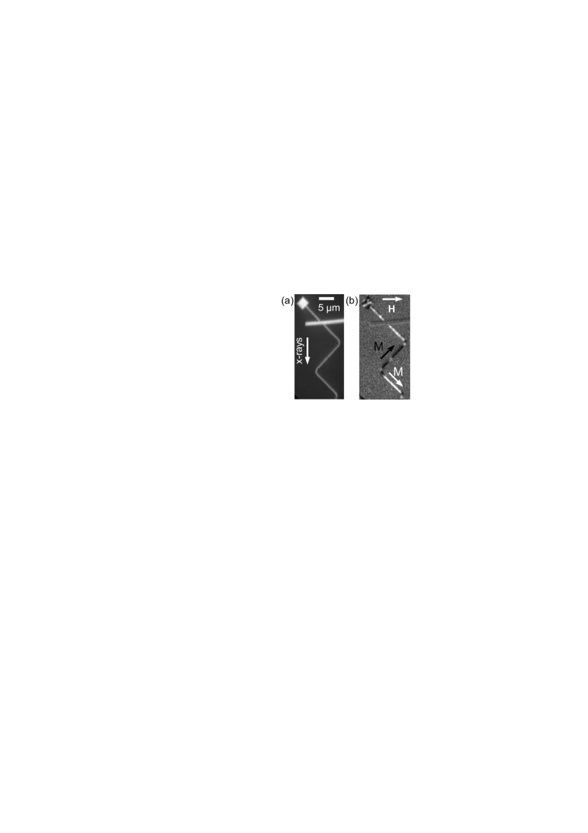
Before introducing the samples into the PEEM microscope, we applied an in-plane magnetic field of 400 mT perpendicularly to the zigzag long axis. The remanent magnetic state obtained for a 400 nm wide, 90∘ angle zigzag nanostripe is shown in Fig. 1(b). The contrast is given by the projection of the magnetization on the beam direction, i.e., white (black) domains have their magnetization pointing downwards (upwards), along the stripes. The magnetization is nearly saturated in the straight sections, but a black-white-black-white contrast is visible at the bends. The magnetization in the straight sections of the buried Co layer is expected to be parallel to the FeNi magnetization, leading to domain walls at the bends. These head-to-head or tail-to-tail domain walls lead to strong magnetostatic effects that induce a local antiparallel alignment between Co and FeNi layers in the vicinity of the Co DW Vogel2007 . In the straight sections, these magnetostatic interactions caused by Co domain walls should not be present.
In Fig. 2, we show current-induced DW motion in a 400 nm wide stripe with zigzag angles of 120∘. The initial domain structure was obtained after application of several magnetic field and current pulses. Domain wall pinning in these structures is quite strong, and several attempts to induce domain wall motion with current pulses were made before reproducible motion could be obtained. The domain structure in Fig. 2(a) could be obtained reproducibly by applying 50 ns long magnetic field pulses in the plane of the samples, to the left in the figure, with an amplitude of 50 mT. Starting from this initial state, we applied current pulses with different amplitudes and lengths, in order to determine the DW velocity and the threshold current in this section. Figure 2(b) shows the domain structure obtained after applying one 100 ns long current pulse with an amplitude of , a value below which no DW motion was detected for these relatively short pulses. This threshold current pulse causes a displacement of the domain wall from position A to position B in the images. A consecutive pulse with the same amplitude and length induces a further movement of the same domain wall in the same direction, from B to C [Fig. 2(c)]. Note that in these images only one DW moves for the applied amplitude of the current, showing that the pinning strengths can strongly differ at different positions in the nanostripe. The free motion of the FeNi DW over section A-C in Fig. 2 indicates that pinning in this section is relatively small.
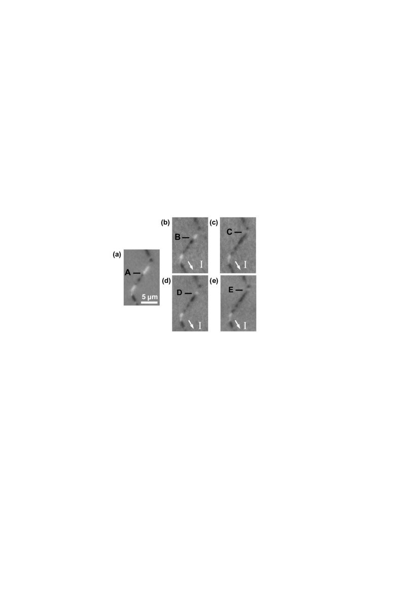
The first pulse causes a CIDM of , the second pulse , resulting in a domain wall velocity of about . The current density in the FeNi layer corresponding to the pulse is if we consider a uniform current distribution through the trilayer stack and if we suppose that the current density is proportional to the conductivity in each layer Laribi2007 . The value of gives thus an upper bound for the current density in the FeNi layer. In Figs. 2(d) and 2(e), we show results of measurements using current pulses with the maximum available amplitude of (corresponding to a current density of in the FeNi layer, or for non-uniform current distribution) and lengths of 15 and 20 ns, in both cases starting from the initial state shown in Fig. 2(a). The CIDM for the 15 and 20 ns pulses are and , showing that in this section of the nanostripe the displacement is about proportional to the pulse length. The resulting DW velocities are and , respectively. This result clearly shows that for this trilayer system the current-induced domain wall velocities between pinning sites are above literature values for single FeNi layers Hayashi2007a , for current densities that are at least a factor two smaller. The above results for strongly different pulse lengths indicate that for this section the displacements are proportional to the pulse length. This suggests that DW movement takes place only during the current pulse and that movements after the current pulse, for instance due to attractive potential wells, are small. Domain wall pinning can be caused by edge roughness induced by the lithography, stray fields of domain walls in the Co layer, interface roughness or grain boundaries. Scanning electron microscopy of our structures indicates a lateral roughness smaller than 1 nm. Roughness of the Cu/FeNi interface should be small with respect to the total FeNi layer thickness of 5 nm. Pinning at grain boundaries could be reduced using amorphous layers of CoFeB instead of FeNi Laribi2007 .
In general, experimental results of current-induced DW dynamics are described (at least qualitatively) using a phenomenological model with two components for the spin transfer torque, i.e., the adiabatic and the non-adiabatic torque. In the simplest approach of a 1D domain wall model Thiaville2005 , the DW velocity is expressed as where is the rate of spin angular momentum transfer from the conduction electrons to the local moments in the domain wall [ where is the current density and its polarization rate Thiaville2005 ]. Several experiments indicate a value of the non-adiabaticity parameter close to , the damping term Beach2006 ; Meier2007 . However, recently Hayashi et al. Hayashi2007a observed a maximum DW velocity of 110 m/s (for ) at zero magnetic field in 300 nm FeNi nanostripes. This velocity is larger than the spin angular momentum transfer rate for any (for , is about 75 m/s and ). Using the same parameters, our current density would lead to a spin transfer rate of about 25 m/s. The only way to explain our measured velocity of 175 m/s within this model would be to assume a of about 7. Such a very large non-adiabaticity seems unlikely and other spin transfer mechanisms must be considered to explain our high DW velocities.
A specificity of our spin-valve structures is that part of the incident spin flux in the FeNi layer is transformed, in the region around the DW, into spin accumulation in the Cu and Co layers. This spin accumulation in the Cu spacer layer below the DW induces a vertical (Current Perpendicular to the Plane or CPP) spin current that flows into the DW and exerts an additional torque on the DW. This situation is somewhat similar to that of spin transfer in the CPP geometry of magnetic pillars. Our results suggest that the yield of this additional vertical spin transfer channel is much higher than the yield of the in-plane spin transfer channel, as predicted recently by micromagnetic simulations on similar nanostructures containing a single DW Khvalkovskiy2008 . Our direct observation of high velocity current-induced DW motion confirms the potential of these trilayer systems for applications in DW-based magnetic memories and logic devices.
Acknowledgements.
We acknowledge the technical support of E. Wagner, P. Perrier, D. Lepoittevin, and L. Delrey, as well as the experimental help of S. Pairis, T. Fournier, and W. Wernsdorfer. We are grateful to A. Khvalkovskiy, A. Anane, and J. Grollier for discussions. E.J. and J.C. acknowledge financial support through projects HF2007-0071, MAT2006-13470, and CSD 2007-00010. V.U. was financially supported by the grants No. MSM0021630508 and No. KAN400100701. This work was partially supported by the ANR-07-NANO-034 ‘Dynawall’.References
- (1) C. Marrows: Adv. Phys. 54 (2005) 585.
- (2) L. Berger: J. Appl. Phys. 55 (1984) 1954.
- (3) J. Grollier, P. Boulenc, V. Cros, A. Hamzic, A. Vaurès, A. Fert, and G. Faini: Appl. Phys. Lett. 83 (2003) 509.
- (4) A. Yamaguchi, T. Ono, S. Nasu, K. Miyake, K. Mibu, and T. Shinjo: Phys. Rev. Lett. 92 (2004) 077205.
- (5) C. Lim, T. Devolder, C. Chappert, J. Grollier, V. Cros, A. Vaurès, A. Fert, and G. Faini: Appl. Phys. Lett. 84 (2004) 2820.
- (6) M. Kläui, P.O. Jubert, R. Allenspach, A. Bischof, J. A. C. Bland, G. Faini, U. Rüdiger, C. Vaz, L. Vila, and C. Vouille: Phys. Rev. Lett. 95 (2005) 026601.
- (7) D. Ravelosona, D. Lacour, J. Katine, B. Terris, and C. Chappert: Phys. Rev. Lett. 95 (2005) 117203.
- (8) M. Kläui, M. Laufenberg, L. Heyne, D. Backes, U. Rüdiger, C. Vaz, J. A. C. Bland, L. Heyderman, S. Cherifi, A. Locatelli, T. Mentes, and L. Aballe: Appl. Phys. Lett. 88 (2006) 232507.
- (9) M. Yamanouchi, J. Ieda, F. Matsukura, S. Barnes, S. Maekawa, and H. Ohno: Science 317 (2007) 1726.
- (10) S. Laribi, V. Cros, M. Muñoz, J. Grollier, A. Hamzić, C. Deranlot, A. Fert, E. Martínez, L. López-Díaz, L. Vila, G. Faini, S. Zoll, and R. Fournel: Appl. Phys. Lett. 90 (2007) 232505.
- (11) M. Hayashi, L. Thomas, C. Rettner, R. Moriya, Y. Bazaliy, and S. S. P. Parkin: Phys. Rev. Lett. 98 (2007) 037204.
- (12) H. Tanigawa, K. Kondou, T. Koyama, K. Nakano, S. Kasai, N. Ohshima, S. Fukami, N. Ishiwata, and T. Ono: Appl. Phys. Express 1 (2008) 011301.
- (13) A. Vanhaverbeke, A. Bischof, and R. Allenspach: Phys. Rev. Lett. 101 (2008) 107202.
- (14) T. Koyama, G. Yamada, H. Tanigawa, S. Kasai, N. Ohshima, S. Fukami, N. Ishiwata, Y. Nakatani, and T. Ono: Appl. Phys. Express 1 (2008) 101303.
- (15) T.A. Moore, I.M. Miron, G. Gaudin, G. Serret, S. Auffret, B. Rodmacq, A. Schuhl, S. Pizzini, J. Vogel, and M. Bonfim: Appl. Phys. Lett. 93 (2008) 262504.
- (16) G. Tatara and H. Kohno: Phys. Rev. Lett. 92 (2004) 086601.
- (17) Z. Li and S. Zhang: Phys. Rev. Lett. 93 (2004) 127204.
- (18) A. Thiaville, Y. Nakatani, J. Miltat, and Y. Suzuki: Europhys. Lett. 69 (2005) 990.
- (19) D. Allwood, G. Xiong, C. Faulkner, D. Atkinson, D. Petit, and R. Cowburn: Science 309 (2005) 1688.
- (20) S. S. P. Parkin, M. Hayashi, and L. Thomas: Science 320 (2008) 190.
- (21) A. Locatelli, and E. Bauer: J. Phys.: Condens. Matter 20 (2008) 093002.
- (22) J. Vogel, W. Kuch, J. Camarero, K. Fukumoto, Y. Pennec, M. Bonfim, S. Pizzini, F. Petroff, A. Fontaine, and J. Kirschner: J. Appl. Phys. 95 (2004) 6533.
- (23) J. Vogel, S. Cherifi, S. Pizzini, F. Romanens, J. Camarero, F. Petroff, S. Heun, and A. Locatelli: J. Phys.: Condens. Matter 19 (2007) 476204.
- (24) G. S. D. Beach, C. Knutson, C. Nistor, M. Tsoi, and J. L. Erskine: Phys. Rev. Lett. 97 (2006) 057203.
- (25) G. Meier, M. Bolte, R. Eiselt, B. Krüger, D.H. Kim, and P. Fischer: Phys. Rev. Lett. 98 (2007) 187202.
- (26) A. Khvalkovskiy, K. Zvezdin, Y. Gorbunov, A. Zvezdin, V. Cros, and J. Grollier, arXiv:0806.2369v1.