Termination Control of the Interface Dipole in La0.7Sr0.3MnO3/Nb:SrTiO3 (001) Schottky Junctions
Abstract
In order to investigate the interface termination dependence of perovskite band alignments, we have studied the Schottky barrier height at La0.7Sr0.3MnO3/Nb:SrTiO3 (001) heterointerfaces. As the Nb:SrTiO3 semiconductor was varied from TiO2 termination to SrO termination by variable insertion of a SrMnO3 layer, a large systematic increase in the Schottky barrier height was observed. This can be ascribed to the evolution of the interface dipole induced to screen the polar discontinuity at the interface, which gives a large internal degree of freedom for tuning band diagrams in oxides.
pacs:
73.40.Sx, 73.40.Ei, 73.40.CgThere has been burgeoning recent interest in the electronic structure of complex oxide heterointerfaces. Technical advances in oxide thin film growth allow the fabrication of structures with atomic scale precision, and together with theoretical advances, a host of new interface electronic states have been found and/or predicted Okamoto and Millis (2004); Ohtomo and Hwang (2004); Popovic and Satpathy (2005); Lee and MacDonald (2006); Pentcheva and Pickett (2007); Reyren et al. (2007); Ruegg et al. (2007); Smadici et al. (2007); Chaloupka and Khaliullin (2008). Fundamental to this endeavor is knowledge of band lineups, which is crucial for the design of new interface states Lee and MacDonald (2006), as well as the engineering of oxide devices. Compared to conventional semiconductors and metals, however, oxide heterointerfaces are far less understood Yunoki et al. (2007).
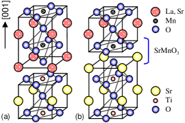
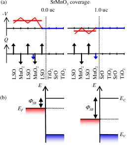
In addition to improving the basic knowledge of complex oxide work functions, electron affinities, etc., there are also structural degrees of freedom at their interfaces which have been little explored. For example, the heterointerface between two (001)-oriented perovskites with different cations can have two different interface terminations (Fig. 1). Given the partially ionic nature of oxides, the different terminations could have significantly different interface dipoles, thus changing the band lineup across the interface. In order to experimentally investigate this effect, we have studied the Schottky interface between the ferromagnetic metal La0.7Sr0.3MnO3 and the n-type semiconductor Nb-doped SrTiO3 (0.05 wt % doped). In addition to providing a model system for these studies, this interface is of strong interest in magnetic tunnel junctions Sun et al. (1996), magnetic field sensitive diodes Nakagawa et al. (2005), and for enhanced photocarrier injection Katsu et al. (2000).
In this paper, we report the investigation of the Schottky barrier height (SBH) in (001)-oriented La0.7Sr0.3MnO3/Nb:SrTiO3 Schottky junctions as 0 - 1 unit cell (uc) of SrMnO3 is inserted at the interface. By growing a La0.7Sr0.3MnO3 film directly on TiO2-terminated Nb:SrTiO3, a MnO2/La0.7Sr0.3O/TiO2 interface is formed [Fig. 1(a)]. Alternatively, by first growing 1 uc of SrMnO3 before La0.7Sr0.3MnO3 deposition, the MnO2/SrO/TiO2 interface is formed [Fig. 1(b)], which is equivalent to the deposition of La0.7Sr0.3MnO3 on the alternative SrO-terminated Nb:SrTiO3 surface Hotta et al. (2007). The deposition of a fractional unit cell of SrMnO3 allows the study of the evolution of the SBH between these endpoints, which was probed using current-voltage (I-V), capacitance-voltage (C-V), and internal photoemission (IPE) measurements. All experiments indicate a systematic increase in the SBH by changing the termination layer at the interface. Although this result is difficult to understand within a Schottky-Mott Sze (1981) or Bardeen Bardeen (1947) framework for metal-semiconductor interfaces, a simple consideration of the evolution of the screening dipole at the interface explains this trend, which is expected to be quite general for metal-semiconductor and metal-insulator perovskite heterointerfaces.
The heterojunctions were fabricated by pulsed laser deposition using a KrF excimer laser with a laser fluence of 0.22 J/cm2, substrate temperature of 850 ∘C, and an oxygen partial pressure of 1 10-3 Torr, as previously optimized Song et al. (2008) . The interface termination was varied by deposition of a calculated thickness of SrMnO3 (SrMnO3 = 0.0, 0.3, 0.6, 1.0 uc), for which the deposition rate was calibrated with reflection high energy electron diffraction (RHEED) prior to the fabrication of the final structures. After the deposition of SrMnO3, 100 uc of La0.7Sr0.3MnO3 was deposited by monitoring the RHEED oscillations. Temperature dependent magnetization measurements give Curie temperatures 360 K in all cases. Ohmic contacts to the La0.7Sr0.3MnO3 and the Nb:SrTiO3 were made by evaporated gold films and In ultrasonic soldering, respectively, contacting an array of junctions each 0.25 mm2 in area. All the measurements were carried out at room temperature and the polarity of the applied bias is defined as positive when applied to the La0.7Sr0.3MnO3.
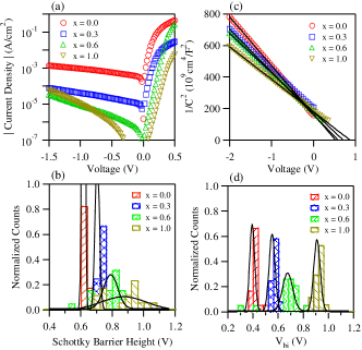
Figure 2(a) shows typical I-V characteristics on a semi-logarithmic scale for samples with different SrMnO3 coverage. Clear rectifying behavior was observed in all cases with forward biased current density systematically decreasing with increase in SrMnO3 coverage. The barrier height obtained from the I-V characteristics () was calculated based on thermoionic emission by fitting the forward biased region of the I-V characteristics. Here a Richardson constant of 156 AK-2 was used Sroubek (1970). In order to obtain reliable statistics, 12 - 19 junctions were sampled for each composition. The obtained SBHs are summarized in a histogram shown in Fig. 2(b) from which it is apparent that an increase in the SBH is observed as a function of SrMnO3 coverage. Considering the exponential dependence of the current on the SBH, the increase in the barrier height is consistent with the systematic decrease in the forward biased current shown in Fig. 2(a).
The reverse biased junction capacitance characteristics at 1 kHz are presented in a - plot as shown in Fig. 2(c). No frequency dependence was found for the capacitance from 20 Hz - 10 kHz, above which the junction RC roll-off was observed. All samples showed a linear dependence on the applied voltage, from which the built-in potential () was calculated, as summarized in a histogram shown in Fig. 2(d). The variance in is smaller than that in , which is a reasonable consequence of the difference in measurement technique. The charge modulation at the edge of the depletion region far away from the interface in C-V tends to capture the spatial average of the barrier height, whereas in I-V the carriers surmount the interface barrier, making it more sensitive to the spatial distribution of the potential at the interface.
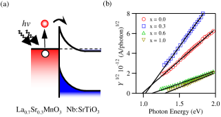
Based on these results, IPE was measured directly through the La0.7Sr0.3MnO3 film (the Au film and electrode was mounted at the edge of the junction) for each composition as shown in Fig. 3. The details of the experimental configuration have been given previously Hikita et al. (2007). The square root of the photoyield , the photocurrent normalized by the incident photon count, is plotted against the incident photon energy. All samples exhibited a linear response of , justifying the application of Fowler’s equation to the emission process Fowler (1931), from which the barrier height is extrapolated.
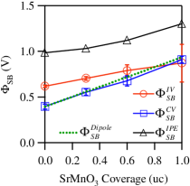
The SBHs obtained from the three independent measurements are summarized in Fig. 4. For I-V and C-V, the mean values obtained from the Gaussian fits to the histograms were used. Note that the barrier heights extracted from Vbi determined by C-V measurements have been corrected for the energy difference between the conduction band minimum and the Fermi level in the Nb:SrTiO3 as discussed in Ref. Hikita et al. (2007), which is a small correction here ( 8.1 mV). All measurements exhibit a systematic increase in the SBH as a function of SrMnO3 coverage at the interface. Although commonly underestimates the SBH due to tunneling contributions or barrier inhomogeneities, the large discrepancy between and is in contrast to the close correspondence of these measurements found for SrRuO3/Nb:SrTiO3 junctions Hikita et al. (2007). A similar contrast between La0.6Sr0.4MnO3/Nb:SrTiO3 and SrRuO3/Nb:SrTiO3 interfaces was observed using photoemission spectroscopy Minohara et al. (2007). For our data, the lack of a low-frequency dispersion to the capacitance indicates that we are not dominated by low-lying trap states. Nevertheless, the quantitative difference between and indicates the presence of fluctuating dipoles at the interface. We turn now to consider the origin of these dipoles, and the systematic increase in the SBH.
First we consider established semiconductor models for Schottky barrier formation. In the simplest Schottky-Mott model of a metal-semiconductor junction, the SBH is purely determined by the difference in the work function of the metal () and the electron affinity () of the semiconductor Sze (1981), and hence cannot capture any termination dependence of the SBH. The classical Fermi level pinning mechanism based on the surface states of semiconductors proposed by Bardeen Bardeen (1947) does not capture variations in metal screening discussed below. Recently, a bond polarization model has been developed Tung (2001), which incorporates both bulk and interface contributions. The interface specific properties are incorporated by electric dipoles generated by the abrupt break in the periodicity of the crystal potential. For an interface between a metal and an n-type semiconductor, the SBH is expressed as Tung (2001),
| (1) |
where
| (2) |
Here is the semiconductor band-gap, the number of interface metal-semiconductor bonds (dipoles), the metal-semiconductor bonding distance, the dielectric constant at the interface, the specific Coulomb interaction between the neighboring atoms at the interface, and the electronic charge. Given that the possible range of is too small to account for the shifts we have observed, is the only parameter linearly varying the SBH, and it is reasonable to conclude that the dipole density at the interface, or the strength of the interface dipole, decreased with SrMnO3 coverage. The limitation of the bond polarization model for our purposes is that it was established for application to covalent semiconductor interfaces, in which the concept of a number of "chemical bonds" at the interface is justified. However, for more ionic semiconductors, such as the case here, the concept of chemical bonds becomes ambiguous because the cohesion of the lattice is dominated by the Madelung energy in the whole crystal rather than local atomic bonds. We discuss below one possible picture of the interface dipole by considering the polarity mismatch at the interface.
Because the present interface systematically changes from MnO2/La0.7Sr0.3O/TiO2 to MnO2/SrO/TiO2, the sheet charge density shifts from -0.7q / +0.7q / 0q to -0.7q / 0q / 0q, assuming a fully ionic charge assignment using the nominal bulk valence for each grown layer, creating a polar discontinuity at the interface. In order to avoid a diverging electrostatic potential arising from the interface, -/+0.35q extra charge is required at the two interfaces, respectively. Whereas previous considerations of this effect between two insulators were discussed in terms of electronic reconstructions Okamoto and Millis (2004); Popovic and Satpathy (2005); Ohtomo and Hwang (2004); Lee and MacDonald (2006); Pentcheva and Pickett (2007); Ruegg et al. (2007); Smadici et al. (2007) , here the interface between a metal and a semiconductor is better framed in terms of metallic screening by the La0.7Sr0.3MnO3 — the Nb:SrTiO3 side of the interface being fully depleted.
To estimate the length scale for screening, the Thomas-Fermi screening length is 0.31 nm, using a bulk carrier density of 5.1 1021 cm-3, a dielectric constant of 30 Shannon (1993), and an electron effective mass of 2.5 Okuda et al. (1998). This length scale, less than a unit cell, corresponds to changing the valence of Mn at the first interface layer in the simplest ionic assignment. Thus, as depicted in Fig. 5, the first MnO2 layer of La0.7Sr0.3MnO3 will have extra screening charge. Even after this charge compensation, a finite electrostatic potential remains inside La0.7Sr0.3MnO3 relative to Nb:SrTiO3, giving an interface dipole which linearly varies with the interface termination.
The variation in the band-offset induced by the difference in the termination at the interface can be estimated using the charge assignment shown in Fig. 5. Using the previous values used for the Thomas-Fermi estimate, the evolution of the SBH arising from this ionic dipole is given in Fig. 4, referenced to the Schottky-Mott relation Minohara et al. (2007). The electrostatic potential difference between the two end-member interfaces is 0.54 V. This value, as well as the linearly increasing SBH with varying interface termination, are in reasonable agreement with the experimentally determined trends.
In summary, we have presented experiments finding a systematic increase in the Schottky barrier height in La0.7Sr0.3MnO3/Nb:SrTiO3 (001) heterojunctions as the Nb:SrTiO3 semiconductor was varied from TiO2 termination to SrO termination, and a simple model for interface dipole formation which captures this trend. It should be noted that the ionic limit discussed here is just as oversimplified as the covalent limit used in the bond polarization model; the real system is intermediate between these two extremes. In addition to hybridization effects, a more realistic estimate of the interface dipole requires better understanding of the relevant on these very short length scales. Ab initio calculations such as recently performed for ultrathin perovskite superlattices should give more quantitative insight Stengel and Spaldin (2006); Hamann et al. (2006). Nevertheless, this basic framework for interface dipole formation is quite general, and should assist in the design of oxide heterostructures and control of their band alignments.
This work was supported by the TEPCO Research Foundation and a Grant-in-Aid for Scientific Research on Priority Areas.
References
- Okamoto and Millis (2004) S. Okamoto and A. J. Millis, Nature (London) 428, 630 (2004).
- Ohtomo and Hwang (2004) A. Ohtomo and H. Y. Hwang, Nature 427, 423 (2004).
- Popovic and Satpathy (2005) Z. S. Popovic and S. Satpathy, Phys. Rev. Lett. 94, 176805 (2005).
- Lee and MacDonald (2006) W. C. Lee and A. H. MacDonald, Phys. Rev. B 74, 075106 (2006).
- Pentcheva and Pickett (2007) R. Pentcheva and W. E. Pickett, Phys. Rev. Lett. 99, 016802 (2007).
- Reyren et al. (2007) N. Reyren, S. Thiel, A. D. Caviglia, L. F. Kourkoutis, G. Hammerl, C. Richter, C. W. Schneider, T. Kopp, A.-S. Ruetschi, D. Jaccard, et al., Science 317, 1196 (2007).
- Ruegg et al. (2007) A. Ruegg, S. Pilgram, and M. Sigrist, Phys. Rev. B 75, 195117 (2007).
- Smadici et al. (2007) S. Smadici, P. Abbamonte, A. Bhattacharya, X. Zhai, B. Jiang, A. Rusydi, J. N. Eckstein, S. D. Bader, and J.-M. Zuo, Phys. Rev. Lett. 99, 196404 (2007).
- Chaloupka and Khaliullin (2008) J. Chaloupka and G. Khaliullin, Phys. Rev. Lett. 100, 016404 (2008).
- Yunoki et al. (2007) S. Yunoki, A. Moreo, E. Dagotto, S. Okamoto, S. S. Kancharla, and A. Fujimori, Phys. Rev. B 76, 064532 (2007).
- Sun et al. (1996) J. Z. Sun, W. J. Gallagher, P. R. Duncombe, L. Krusin-Elbaum, R. A. Altman, A. Gupta, Y. Lu, G. Q. Gong, and G. Xiao, Appl. Phys. Lett. 69, 3266 (1996).
- Nakagawa et al. (2005) N. Nakagawa, M. Asai, Y. Mukunoki, T. Susaki, and H. Y. Hwang, Appl. Phys. Lett. 86, 082504 (2005).
- Katsu et al. (2000) H. Katsu, H. Tanaka, and T. Kawai, Appl. Phys. Lett. 76, 3245 (2000).
- Hotta et al. (2007) Y. Hotta, T. Susaki, and H. Y. Hwang, Phys. Rev. Lett. 99, 236805 (2007).
- Sze (1981) S. M. Sze, Physics of Semiconductor Devices, 2nd ed. (Wiley, New York, 1981).
- Bardeen (1947) J. Bardeen, Phys. Rev. 71, 717 (1947).
- Song et al. (2008) J. H. Song, T. Susaki, and H. Y. Hwang, Adv. Mater. 20, 2528 (2008).
- Sroubek (1970) Z. Sroubek, Phys. Rev. B 2, 3170 (1970).
- Hikita et al. (2007) Y. Hikita, Y. Kozuka, T. Susaki, H. Takagi, and H. Y. Hwang, Appl. Phys. Lett. 90, 143507 (2007).
- Fowler (1931) R. Fowler, Phys. Rev. 38, 45 (1931).
- Minohara et al. (2007) M. Minohara, I. Ohkubo, H. Kumigashira, and M. Oshima, Appl. Phys. Lett. 90, 132123 (2007).
- Tung (2001) R. Tung, Mater. Sci. Eng. R 35, 1 (2001).
- Shannon (1993) R. D. Shannon, J. Appl. Phys. 73, 348 (1993).
- Okuda et al. (1998) T. Okuda, A. Asamitsu, Y. Tomioka, T. Kimura, Y. Taguchi, and Y. Tokura, Phys. Rev. Lett. 81, 3203 (1998).
- Stengel and Spaldin (2006) M. Stengel and N. A. Spaldin, Nature 443, 679 (2006).
- Hamann et al. (2006) D. R. Hamann, D. A. Muller, and H. Y. Hwang, Phys. Rev. B 73, 195403 (2006).