Conductance of a disordered graphene superlattice
Abstract
We study the conductance of disordered graphene superlattices with short-range structural correlations. The system consists of electron- and hole-doped graphenes of various thicknesses, which fluctuate randomly around their mean value. The effect of the randomness on the probability of transmission through the system of various sizes is studied. We show that in a disordered superlattice the quasiparticle that approaches the barrier interface almost perpendicularly transmits through the system. The conductivity of the finite-size system is computed and shown that the conductance vanishes when the sample size becomes very large, whereas for some specific structures the conductance tends to a nonzero value in the thermodynamics limit.
pacs:
68.65.Cd, 73.22.-f, 73.63.-b, 73.40.LqI Introduction
Graphene, a single atomic layer of graphite, has been successfully produced in experiment novoselov , which has resulted in intensive investigations on graphene-based structures, due to the fundamental physics interests that is involved and the promising applications geim . There are significant current efforts devoted to growing graphene epitaxially berger by thermal decomposition of silicon carbide (SiC), or by vapor deposition of hydrocarbons on catalytic metallic surfaces, which could later be etched away, leaving graphene on an insulating substrate. The low energy quasiparticle excitations in graphene are linearly dispersing, and are described by Dirac cones at the edges of the first Brillouin zone. The linear energy-momentum dispersion has been confirmed by recent observations novoselov1 . The slope of the linear relation corresponds the Fermi velocity of chiral Dirac electrons in graphene, which plays an essential role in the Landau-Fermi liquid theory polini and has a direct connection to the experimental measurement.
There are some unusual features of graphene, such as the effects of electron-electron interactions on the ground-state properties yafis , anomalous tunneling effect described by the Klein tunneling, the tunneling through a p-n junctionklein ; katsnelson1 that follows from chiral band states, and the energy-momentum linear dispersion relation. The Klein tunneling predicts that the chiral massless carrier can pass through a high electrostatic potential barrier with probability one, regardless of the height and width of the barrier at normal incidence, which is in contrast with the conventional nonrelativistic massive carrier tunneling where the transmission probability decays exponentially with the increasing of the barrier hight and would depend on the profile of the barrier. greiner ; su ; dombey ; krekora
An exciting experimental development is the ability to apply an electric field effect or submicron gate voltage, in order to illustrate graphene p-n junctions. williams By applying an external gate voltage, the system can be switched from the n-type to the p-type carriers, thereby controlling the electronic properties that give rise to graphene-based nanodevices. Recently, strong evidence for Klein tunneling across potential steps which is steep enough in graphene has been experimentally observed. stander
Clean graphene junctions were predicted to display a number of fascinating physical phenomena, even in the absence of electron-electron interactions. cheianov Interestingly, the Veselago lensing of electric current by a single p-n junction in clean graphene cheianov1 and the Andreev reflection, and the electron to hole conversion at the interface at normal incidence beenakker , have all been predicted theoretically. Such phenomena are predicted to change both quantitatively and qualitatively when disorder is included in the model. For instance, inhomogeneous graphene p-n junction systems were studied using the Thomas-Fermi approximation, including disorder effects, by Fogler and collaborators fogler . They showed that junction resistance is dominated by either ballistic or diffusive contributions, depending on the density of charged impurity and gradient of the carrier density.
In the semiconductor context there are basically a large number of works on the tunneling, which have resulted in the ”obvious” declaration that the electronic properties of semiconductor superlattice are different from those calculated in a single-barrier junction. Moreover, the electronic properties of semiconductor superlattices in the presence of disorder have been studied by several groups diez1 ; adame ; diez2 ; bellani ; esmailpour . Importantly, all the electronic states are localized in the thermodynamic limit for a semiconductor superlattice in the presence of white-noise disorder. diez2
Graphene superlattices, on the other hand, may be fabricated by adsorbing adatoms on graphene surface through similar techniques, by positioning and aligning impurities with scanning tunneling microscopy eigler or by applying a local top gate voltage to graphene. huard Recently, a periodic pattern in the scanning tunneling microscope image has been demonstrated on a graphene on top of a metallic substrate. marchini The transition of hitting massless particles in graphene-based superlattice structure (GSLs) was first studied by Bai and Zhang. bai They showed that the conductivity of the GSLs depends on the superlattice structural parameters. Furthermore, the superlattice structure of graphene nanoribbons has been recently studied by using first-principles density functional theory calculations. sevincli These calculations showed that the magnetic ground state of the constituent ribbons, the symmetry of the junction, and their functionalization by adatoms represent structural parameters to the electronic and magnetic properties of such structures. Recently, novel physical properties of GSLs with one-dimensional (1D) Kronig-Penney type and 2D muffin-tin type potentials were also studied. cheol The results showed that a periodic potential applied by suitably patterned modifications leads to further charge carrier behavior. The propagation of charge carriers through such a superlattice is highly anisotropic, and in extreme cases results in group velocities that are reduced to zero in one direction but are unchanged in the other direction. Moreover, they showed that the density and type of carrier are extremely sensitive to the applied potential.
It would, therefore, be worthwhile to investigate how the conductance of graphene superlattice junctions are affected by structural white noise, and compare the conductances with those calculated for disordered semiconductor superlattice. Due to the conservation of pseudospins in graphene, backscattering process is suppressed at normal incidence, which makes the disordered regions transparent. beenakker
The purpose of this paper is to study the electronic behavior of graphene superlattices p-n junctions by using the transfer-matrix method. The system that we study consists of a sequence of electron-doped graphene as wells, and hole-doped graphene as barriers. We study the effect of the disorder imposed on the size of the barriers in the transmission probability, , through the system as a function of the system size (number of the barriers), together with various incident angles. The dc conductance of the finite-size system takes on a nonzero value of the transmission in some special configurations. Using the finite-size scaling of transmission, we show that the conductance, in the thermodynamic limit, tends to a finite constant for spacial cases.
The rest of this paper is organized as follows. In Sec. II we introduce the models and derive the related transfer matrix. We also explain how we calculate the transmission probability and the dc conductivity. Section III contains our numerical calculations. We conclude in Sec. IV with a brief summary.
II Model and Theory
Consider a system of superlattice p-n junctions in the independent carriers model at zero temperature, and in the absence of carrier-phonon and spin-orbit interactions. The low-energy massless Dirac-band Hamiltonian of graphene in the continuum model can be written asslon ; haldane
where for the inequivalent and valleys at which and bands touch, is an envelope function momentum operator, is the Fermi velocity, and is a Pauli matrix that acts on the sublattice pseudospin degree of freedom. The total Hamiltonian of a massless carrier in a special geometry is written as, where is the graphene-based superlattice potential which is modeled as described below.
II.1 Superlattice Model
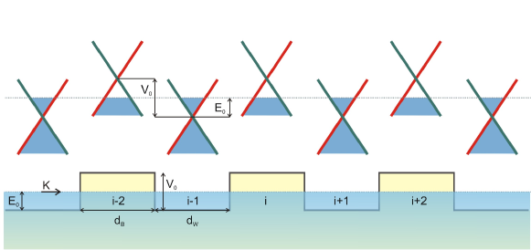
We consider superlattice p-n junctions in a graphene-based structure. The system consists of two kinds of graphene with different potentials, the first being an electron-doped graphene with thickness , while the second is a hole-doped part with thickness , standing alternately. The potential for the electron- and hole-doped graphene are and zero, respectively. The energy of the incident particle is with the wavelength across the barriers, in such a way that the Fermi level lies in the conduction band outside the barrier and the valence band inside it, i.e., , as shown in Fig. 1. The growth direction is taken to be the axis which is designed as the superlattice axis. In order to neglect the strip edges, we assume that the width of the graphene strip is much larger than . We set disorder situations in which the value of fluctuates around its mean value, given by . In the model the fluctuations are given by, , where is a set of uncorrelated random variables or white noise with the box distribution, , and is the site index. Here, the is the disorder strength.
We consider graphene-based superlattice potential in a simple model as
| (3) |
where is the position of barriers’ center. The model is similar to the potential of semiconductor superlattices that has been used by other groups. esmailpour
II.2 DC conductivity
Let us now consider the case in which the incident massless electron in the GSLs propagates at angle along the axis (see Fig. 1) and, therefore, the Dirac spinor components, and , which are the solutions to the Dirac Hamiltonian, can be expressed bai as:
| (4) |
where
| (5) |
and
| (6) |
In order to calculate the transmission coefficients, we use the transfer-matrix method katsnelson . To this end, we apply the continuity of the wave function at the boundaries, and construct the transfer matrices as follows
| (11) | |||
| (14) |
where and are the reflection and transmission coefficients of the system that consists of barriers, and is the transfer matrix given by
| (15) | |||
| (18) |
where also is a transfer matrix from site to and are given by
| (19) | |||||
where is the length of system at -th boundary and moreover,
| (20) |
It is evident that , and that it can be calculated from Eq. (11) for a given . When the transmission coefficients are calculated, the conductivity of system is computed by means of the Büttiker formula, datta taking the integral of over the angle
| (21) |
where with being the width of the graphene strip along the direction.
III Results and Discussion
Let us first calculate the transmission probability and study the electronic properties of disordered GSLs as a function of the strength of disorder introduced in the system. We consider the width of barriers as a random variable, so that the length of system in the numerical calculations will be . In all the numerical calculations, we assumed nm, while the wavelength of the incident particle is set by nm, or, equivalently, the energy of the carrier, meV. In all of the calculations we used, meV, unless otherwise specified. The number of realization of the random configurations is about 500.
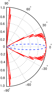
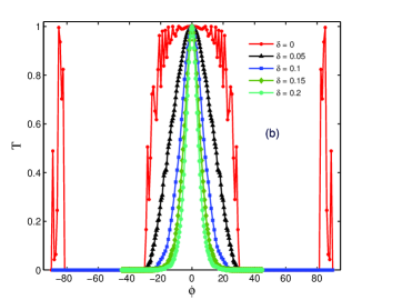
Figure 2 shows the transmission probability, , of the incident electrons hitting a GSLs, as a function of the angle for several values of the disorder strength, . The number of the barriers in the figure is, , with nm. It is clear that, the transmission decreases by increasing the disorder for all the angles, apart from the strictly normal incidence case, . This is physically understandable due to the Klein tunneling process in graphene, where the backscattering process is suppressed. Moreover, the massless carriers with incident angle close to normal incidence can survive in the presence of disorder, while the width of the angles around the normal incidence decreases with increasing strength of the disorder as well.
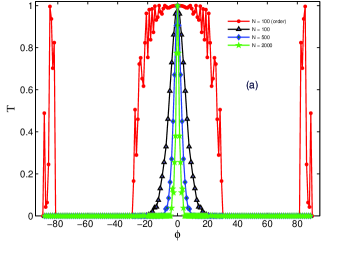
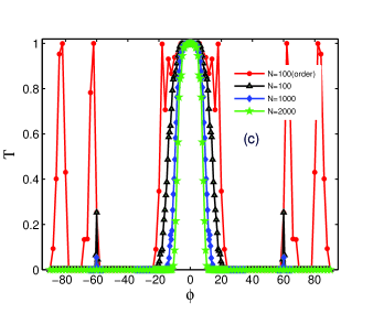
In order to understand the finite-size effect and the effect of the width of the wells, the transmissions probability of a massless particle through the system were calculated as a function of the incident angle. The results are shown in Fig. 3 for several sizes at . In Fig. 3(a) we set nm. The transmission decreases with increasing system size for all the angels, except again at . This behavior is in contrast with a clean GSLs result, where the number of the peaks increases by increasing the number of the barriers. bai In Fig. 3(b) the width of the wells is set to, nm. Two sharp peaks in the transmission are obtained that disappear in Fig. 3(a). Furthermore, in the case with nm there is only one angle, , that the transmission survives in the presence of the disorder, whereas under other angles the transmissions are suppressed. Meanwhile, there is clearly a wide domain around for which the transmission survives, and is larger than the one shown in Fig. 3(b). The width of the domain decreases with increasing strength of the disorder. It is worthwhile to note qualitatively that for , when we have the condition that, ( is an integer), the transmission has finite values at angles different from . This is due to the resonance process in a system with barriers.
We also studied how disorder, introduced in the GSLs, affects the conductivity of the system. Hence, we also calculated numerically the dc conductivity by using Eq. (21), with the white-noise structural disorder imposed on the system. Figure 4 shows the dc conductance of the GSLs as a function of for various strengths of the disorder, . As shown in the figure, the conductivity of the GSLs decreases by increasing the strength of the disorder. However, the conductivity approaches a finite value, i.e., the existence of a finite conductivity in finite-size disordered GSLs should be expected. In general, the resonance condition is given by a function that yields, . For instance, for the case , the condition yields, , as a result of which would be an oscillating function of . Note that is determined by . Consequently, this leads to a finite dc conductivity which is an oscillating function of . The observation of conductance oscillations in extremely narrow graphene hetrostructures has been observed experimentally. young
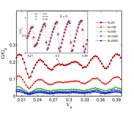
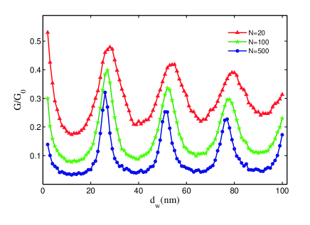
In Fig. 5 the conductivity of the system is plotted as a function of , where the width of the wells is nm with . The conductivity decreases with increasing the size of system. The inset in the figure shows the conductivity of a clean GSLs as a function of for several system sizes. It indicates that the dc conductance of clean superlattice behaves uniquely for different sizes, but in a disordered GSLs it decreases by increasing the size of system, as shown in Fig. 5. At a constant strength of the disorder, changing may also change the conductivity, as depicted in Fig. 6. It demonstrates that the conductivity varies periodically with increasing . As a result, in the disordered GSLs, the dc conductance of finite-size systems depends on the structural parameters, especially .
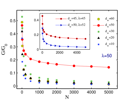
To compute all results that have been presented so far, we considered a system of finite size. Next, we wish to calculate the finite-size scaling of . For this purpose, we calculated the conductivity as a function of the system size. The results are summarized in Fig. 7. Importantly, the conductivity vanishes by a simple power law, except for the case for which, nm. In general, for the conductivity approaches a finite value as becomes large.
In order to examine such results better, we also calculated the for a case for which nm. We found that the conductance tends to a constant in the thermodynamic limit. the numerical data are fitted by using
| (22) |
where , , and are constants. is the asymptotic value of in the thermodynamic limit, . As a result, for the case nm we obtain , , and ; for nm we obtained, , , and , and , and for nm. In all the case the regression was with , indicating very accurate fits. Note that is zero for small , but tends to a nonzero constant for nm.
IV Conclusion
We studied numerically the dc conductance of a discorded graphene superlattice p-n junctions for various values of the strength of structural disorder imposed on the material. It was shown that there exists a width around the normal incidence angle for which the transmission becomes finite in the presence of structural white-noise disorder. That is, the white-noise disorder gives rise the largest number of the peaks in the transmission, suppressed in the thermodynamic limit but quasiparticles which approach almost perpendicularly to the barriers transmit through the material. We also calculated the conductivity of a finite-size disordered system and showed that the conductivity decreases by increasing the system size but that there are cases for which the conductance approaches a nonzero value. This result is in contrast with the case of a clean (ordered) GSLs. bai Furthermore, the results of the finite-size scaling computations predict a zero conductance for all the GSLs, except for some special values for which , where is an integer, in which case the conductance tends to a nonzero constant in the thermodynamic limit.
Apparently, such a feature is independent of the value of . Consequently, we predict a finite conductivity for a disordered GSLs when the wavelength of incident particle is equal to . These results are in complete contrast with those calculated for disordered semiconductor superlattice which become insulator. diez1 ; diez2 ; bellani Our finding for the dc conductance of the GSLs should be important to the design of electronic nano-devices based on graphene superlattices. It would probably worthwhile to extend the present work to the case in which a correlated noise is used. In this case one must replace the white-noise with a proper short- or long-range correlated noise.
Acknowledgements.
R. A. would like to thank the International Center for Theoretical Physics, Trieste for its hospitality during the period when part of this work was carried out. A. E and N. A are supported by the IPM grant.References
- (1) K. S. Novoselov, A. K. Geim, S. V. Morozov, D. Jiang, Y. Zhang, S. V. Dubonos, I. V. Grigorieva, and A. A. Firsov, Science 306, 666 (2004).
- (2) A. K. Geim and K. S. Novoselov, Nature Mater. 6, 183 (2007); A. K. Geim and A. H. MacDonald, Phys. Today 60, 35 (2007); A. H. Castro Neto, F. Guinea, N. M. Peres, K. S. Novoselov, and A. K. Geim, Rev. Mod. Phys. 81, 109 (2009).
- (3) C. Berger, Z. Song, X. Li, X. Wu, N. Brown, C. Naud, D. Mayou, T. Li, J. Hass, A. N. Marchenkov, E. H. Conrad, P. N. First, and W. A. de Heer, Science 312, 1191 (2006).
- (4) K. S. Novoselov, E. McCann, S. V. Morosov, V. Fal’ko, M. I. Katsnelson, U. Zeitler, D. Jian, F. Scheden, and A. K. Geim, Nature 438, 197 (2005); Y. Zhang, J. W. Tan, H. L. Stormer, and P. Kim, Nature 438, 201 (2005); Z. Jiang, E. A. Henriksen, L. C. Tung, Y.-J. Wang, M. E. Schwartz, M. Y. Han, P. Kim, and H. L. Stormer, Phys. Rev. Lett. 98, 197403 (2007); A. Bostwick, T. Ohta, T. Seyller, K. Horn, and E. Rotenberg, Nature Phys. 3, 36 (2007); New J. Phys. 9, 385 (2007); M. Mucha-Kruczyński, O. Tsyplyatyev, A. Grishin, E. McCann, V. I. Fal’ko, A. Bostwick, and E. Rotenberg, Phys. Rev. B 77, 195403 (2008); S. Y. Zhou, G.-H. Gweon, A. V. Fedorov, P. N. First, W. A. de Heer, D.-H. Lee, F. Guinea, A. H. Castro Neto, and A. Lanzara, Nature Mat. 6, 770 (2007).
- (5) M. Polini, R. Asgari, G. Borghi, Y. Barlas, T. Pereg-Barnea and A. H. MacDonald, Phys. Rev. B 77, 081411(R) (2008); M. Polini, R. Asgari, Y. Barlas, T. Pereg-Barnea and A. H. MacDonald, Solid State Commun. 143, 58 (2007).
- (6) Y. Barlas, T. Pereg-Barnea, M. Polini, R. Asgari and A. H. MacDonald, Phys. Rev. Lett. 98, 236601 (2007).
- (7) O. Klein, Z. Phys. 53, 157165 (1929).
- (8) M. I. Katsnelson, K. S. Novoselov, and A. K. Geim, Nature Phys. 2 ,620 (2006).
- (9) W. Greiner, B. Mueller, and J. Rafelski, Quantum Electrodynamics of Strong Fields (Springer, Berlin, 1985).
- (10) R. K. Su, G. C. Siu, and X. Chou, J. Phys. A 26, 1001 (1993).
- (11) N. Dombey and A. Calogeracos, Phys. Rep. 315, 41 (1999).
- (12) P. Krekora, Q. Su, and R. Grobe, Phys. Rev. Lett. 92, 040406 (2004).
- (13) J. R. Williams, L. DiCarlo and C. M. Marcus, Science 317, 638 (2007); B. Huard, J. A. Sulpizio, N. Stander, K. Todd, B. Yang, and D. Goldhaber-Gordon, Phys. Rev. Lett. 98, 236803 (2007); B. Özyilmaz, P. Jarillo-Herrero, D. Efetov, D. A. Abanin, L. S. Levitov and P. Kim, Phys. Rev. Lett. 99, 166804 (2007).
- (14) N. Stander, B. Huard, and D. Goldhaber-Gordon, arXiv: 0806.2319.
- (15) V. V. Cheianov and V. I. Fal’ko, Physics. Rev. B 74, 041403(R) (2006); J. M. Pereira, Jr. V. Mlinar, F. M. Peeters, and P. Vasilopoulos, Phys. Rev. B 74, 045424 (2006).
- (16) V . V. Cheianov and V. I. Fal’ko, and B. L. Altshuler, Science 315, 1252 (2007).
- (17) C. W. J. Beenakker, Rev. Mod. Phys. 80, 1337 (2008).
- (18) L. M. Zhang and M. M. Fogler, Phys. Rev. Lett. 100, 116804 (2008); M. M. Fogler, D. S. Novikov, L. I. Glazman, and B. I. Shklovskii, Phys. Rev. B 77, 075420 (2008).
- (19) E. Diez, A. Sánchez, and F. Domínguez-Adame, Phys. Rev. B 50, 14359 (1994).
- (20) F . Domínguez-Adame, A. Sánchez, and E. Diez, Phys. Rev. B 50, 17736 (1994).
- (21) E. Diez, A. Sánchez, and F. Domínguez-Adame, IEEE J. Quantum Electron. 31, 1919 (1995).
- (22) V. Bellani, et. al., Phys. Rev. Lett. 82, 2159 (1999).
- (23) A. Esmailpour, M. Esmaeilzadeh, E. Faizabadi, Pedro Carpena, and M. R. Rahimi Tabar, Phys. Rev. B 74, 024206 (2006).
- (24) H. Hiura, Appl. Surf. Sci. 222, 374 (2004); J. C. Meyer, C. O. Girit, M. F. Crommie, and A. Zettl, Appl. Phys. Lett. 92, 123110 (2008).
- (25) B. Huard, J. A. Sulpizio, N. Stander, K. Todd, B. Yang, and D. Goldhaber-Gordon, Phys. Rev. Lett. 98, 236803 (2007).
- (26) S. Marchini, S. Gunther, J. Wintterlin, Phys. Rev. B76, 075429 (2007); A. L. Vázquez de Parga, F. Calleja, B. Borca, M. C. G. Passeggi, Jr., J. J. Hinarejos, F. Guinea, and R. Miranda, Phys. Rev. Lett. 100, 056807 (2008); I. Pletikosić, M. Kralj, P. Pervan, R. Brako, J. Coraux, A. T. ŃDiaye, C. Busse, and T. Michely, arXiv:0807.2770; Y. Pan, N. Jiang, J. T. Sun, D. X. Shi, S. X. Du, F. Liu, and H.-J. Gao, arXiv:0709.2858.
- (27) C. Bai and X. Zhang, Phys. Rev. B. 76, 075430 (2007).
- (28) H. Sevinçli, M. Topsakal, and S. Ciraci, arXiv: 0711.2414.
- (29) C.-H. Park, L. Yang, Y.-W. Son, M. L. Cohen, and S. G. Louie, Nature Physics 4, 213 (2008).
- (30) J. C. Slonczewski and P. R. Weiss, Phys. Rev. 109, 272 (1958).
- (31) F. D. M. Haldane, Phys. Rev. Lett. 61, 2015 (1988).
- (32) M. I. Katsnelson, Eur. Phys. J. B 51, 157 (2006); J. Tworzydlo, B. Trauzettel, M. Titov, A. Rycerz, and C. W. Beebakker, Phys. Rev. lett. 96, 246802 (2006); M. Titov, Europhys. Lett. 79, 17004 (2007).
- (33) S. Datta, Electronic Transport in Mesoscopic Systems (Cambridge University Press, London, 1995).
- (34) A. F. Young and P. Kim, arXiv: 0808.0855.