Charge Detection in Graphene Quantum Dots
Abstract
We report measurements on a graphene quantum dot with an integrated graphene charge detector. The quantum dot device consists of a graphene island (diameter 200 nm) connected to source and drain contacts via two narrow graphene constrictions. From Coulomb diamond measurements a charging energy of 4.3 meV is extracted. The charge detector is based on a 45 nm wide graphene nanoribbon placed approx. 60 nm from the island. We show that resonances in the nanoribbon can be used to detect individual charging events on the quantum dot. The charging induced potential change on the quantum dot causes a step-like change of the current in the charge detector. The relative change of the current ranges from 10% up to 60% for detecting individual charging events.
Graphene gei07 ; kat07 , the two dimensional sp2 allotrope of carbon is a promising material for the development of future nanoelectronics and quantum information processing tra07 . This is mainly due to high carrier mobilities nov05 ; zha05 and expected long spin lifetimes. Graphene’s gapless electronic structure and predicted Klein tunneling through pn-barriers kat06 makes it hard to confine charge carriers by electrostatic means. However, by etching graphene it is possible to make tunable graphene nanodevices, as it has been shown by the fabrication of graphene nanoribbons che07 ; han07 ; dai08 , interference devices mia07 ; rus08 ; mol08 and graphene quantum dots sta08 ; sta08b ; pon08 . In this paper we present an integrated graphene device consisting of a graphene quantum dot with a nearby graphene nanoribbon acting as a quantum-point-contact-like charge detector. Charge detection techniques fie93 have been shown to significantly extend the experimental possibilities with quantum dot devices. They are e.g. powerful for detecting spin-qubit states elz04 ; pet05 and molecular states in coupled quantum dots dic04 . Furthermore charge detectors have been succesfully used to investigate shot noise on a single electron level and full counting statistics gus06 . This makes charge detection highly interesting for advanced investigation of graphene quantum dots and graphene nanosystems in general.
Fig. 1a shows a scanning force microscope image of the all graphene structure. The quantum dot device consists of two 35 nm wide graphene constrictions separating source (S) and drain (D) contacts from the graphene island (diameter 200 nm). The constrictions and the island are electrostatically tuned independently by two barrier gates (B1 and B2) and a plunger gate (PG), respectively. The highly doped silicon back gate (BG) allows to adjust the overall Fermi level. In addition, we placed a 45 nm wide graphene nanoribbon 60 nm next to the island, which acts as a charge detector (CD), as shown below.
The sample is fabricated by mechanical exfoliation of natural bulk graphite nov04 . Single-layer graphene flakes are transferred to highly doped silicon substrates with a 295 nm silicon oxide top-layer. Electron beam lithography (EBL) is used for patterning the isolated graphene flakes by subsequent Ar/O2 reactive ion etching. A second EBL and a lift-off step is performed to place source, drain electrodes and contacts to the lateral gate electrodes (all 2/50 nm Ti/Au). For the detailed fabrication process and the single-layer graphene identification by Raman spectroscopy we refer to Refs. sta08 ; fer06 ; dav07a .
Measurements were performed in a variable temperature insert cryostat at a base temperature of 1.7 K using low-frequency lock-in techniques.
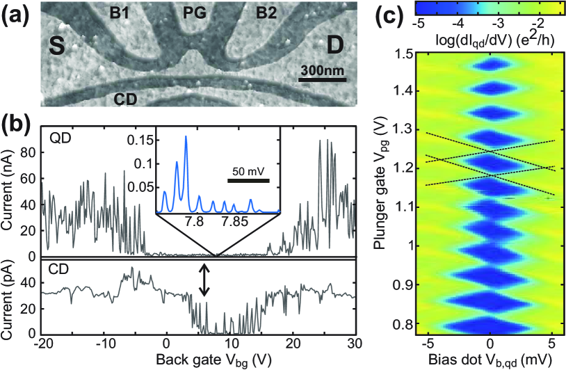
The characterization of the individual devices is shown in Fig. 1b and 1c. Fig. 1b shows the current as a function of the back gate voltage at a temperature of 1.7 K of both, the quantum dot device (upper curve) and the charge detector (lower curve). In both cases we observe a transport gap sta08 extending roughly from -4 V to 15 V and from 4 V to 14 V for the quantum dot, and charge detector, respectively. From high source-drain voltage () measurements (not shown) we estimate the characteristic energy scale of these effective energy gaps to be about 13 meV, and 8 meV, respectively. This is in reasonable agreement with recent measurements on graphene nanoribbons where the transport gap is dominated by the width of the graphene nanostructure sol07 . The large scale current fluctuations are attributed to resonances in the graphene constrictions. By focusing on a smaller back gate voltage range of 150 mV (see inset in Fig. 1b) Coulomb blockade resonances of the quantum dot are resolved in regions where these resonances are suppressed. In Fig. 1c Coulomb diamond measurements of the quantum dot are shown. The differential conductance of the dot is plotted as a function of the bias voltage and plunger gate voltage for a fixed back gate voltage V. From this measurement a charging energy 4.3 meV and a plunger gate lever arm =0.06 is extracted. From further diamond measurements as function of back gate and fixed plunger gate voltage (not shown here) we find a back gate lever arm of =0.34.
After having demonstrated the functionality of both devices independently their joint operation is shown in Figs. 2 and 3 where we demonstrate the functionality and high sensitivity of the graphene charge detector.
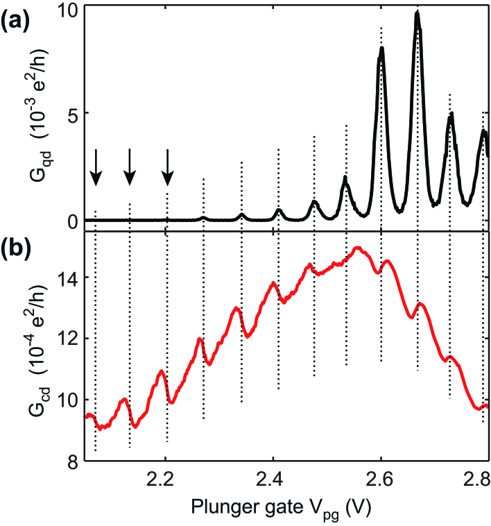
For these measurements the back gate voltage is set to V such that the quantum dot is close to the charge neutrality point (see arrows in Fig. 1b) as well as inside the transport gap of the charge detector. We operate the charge detector in a regime where strong resonances are accessible, in order to make use of steep slopes of the conductance as a function of of the order of 4-6 10-4 ()/100 mV to detect individual charging events on the quantum dot.
Fig. 2a shows almost equidistantly spaced ( mV) Coulomb blockade resonances as function of at V. The strong modulation of the conductance peak amplitudes is due to superimposed resonances in the graphene constrictions defining the island sta08 . In Fig. 2b we plot the simultaneously measured conductance through the nearby charge detector (at a bias voltage of mV) for the same range. On top of the peak-shaped CD resonance we observe conductance steps which are well aligned (see dotted lines) with single charging events on the nearby quantum dot.
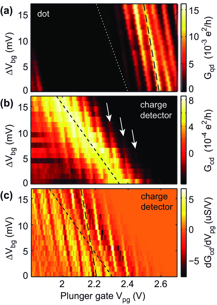
Figs. 3a and 3b show 2D plots of a set of traces corresponding to those shown in Figs. 2a and 2b, taken for different back gate voltages and V. Fig. 5a shows Coulomb blockade resonances in the quantum dot conductance following a relativ lever arm of PG and BG of = 0.18 (see black dashed line). In Fig. 3b these resonances are observed through charge detection and are marked with arrows. The charge detector resonance used for detection can be distinguished from the dot resonances by its larger width and its different slope given by = 0.04 (black dashed line). This reduced slope is due to the larger distance of the CD nanoribbon to the plunger gate ( 350 nm) as compared to the island-plunger gate distance. The modulation of the Coulomb blockade resonances in Fig. 3a is due to resonances in the tunneling constriction located around 300 nm away from the PG (see Fig. 1a). This leads to a slope of 0.08 for these peak modulations (see white dotted line). Independent of this modulation we identify single charging events on the quantum dot as conductance fringes (see arrows in Fig. 3b) on top of the up and down slope of the CD resonance. This can even better be seen by numerical differentiation of vs. , as shown in Fig. 3c. Here the sharp conductance changes due to the charging events in the dot are strongly pronounced, and both relative lever arms to the Coulomb blockade peaks and the constriction resonance in the charge detector are indicated by dashed lines. The detection range can be improved by increasing the bias , leading to a broadening of the constriction resonance, as seen by comparing Fig. 3c with Fig. 2b.
From the measurement shown in Fig. 2b a nanoribbon conductance change of up to 10% can be exctracted for a single charging event. For lower bias voltages (e.g. V) the change in the conductance can be incresed to 60%.
In conclusion, we demonstrated the functionality of an integrated graphene charge detector based on a nanoribbon nearby a graphene quantum dot. We confirm the detection of charging events in regimes where Coulomb blockade resonances can hardly be measured (i.e. resolved) because the current levels are too low (see, e.g., arrows in Fig. 2a). In contrast to state-of-the-art quantum point contact charge detectors we do not make use of slopes to quantized conductance plateaus. We rather use local resonances in the graphene nanoribbon to detect charging. We anticipate, that this technique will play an important role for the investigation of the electron-hole crossover and spin-states in graphene quantum dots.
The authors wish to thank R. Leturcq, P. Studerus, C. Barengo, P. Strasser, A. Castro-Neto and K. S. Novoselov for helpful discussions. Support by the ETH FIRST Lab, the Swiss National Science Foundation and NCCR nanoscience are gratefully acknowledged.
References
- (1) A. K. Geim and K. S. Novoselov, Nat. Mater. 6, 18 (2007).
- (2) M. I. Katsnelson, Mater. Today 10, 20 (2007).
- (3) B. Trauzettel, D.V. Bulaev, D. Loss, and G. Burkard, Nature Physics, 3, 192, (2007).
- (4) K. S. Novoselov, A. K. Geim, S. V. Morozov, D. Jiang, M. I. Katsnelson, I. V. Grigorieva, S. V. Dubonos, and A. A. Firsov, Nature, 438, 197-200, (2005).
- (5) Y. Zhang, Y.-W. Tan, H. L. Stormer, and P. Kim, Nature, 438, 201-204, (2005).
- (6) M. I. Katsnelson, K. S. Novoselov, amd A. K. Geim, Nature Phys. 2, 620 625 (2006).
- (7) Z. Chen, Y. Lin, M. Rooks, and P. Avouris, Physica E, 40, 228, (2007).
- (8) M. Y. Han, B. Özyilmaz, Y. Zhang, and P. Kim, Phys. Rev. Lett., 98, 206805 (2007).
- (9) X. Li, X. Wang, L. Zhang, S. Lee, and H. Dai, Science, 319, 1229 (2008).
- (10) F. Miao, S. Wijeratne, Y. Zhang, U. C. Coskun, W. Bao, and C. N. Lau, Science, 317, 1530 (2007).
- (11) S. Russo, J. B. Oostinga, D. Wehenkel, H. B. Heersche, S. S. Sobhani, L. M. K. Vandersypen, and A. F. Morpurgo, Phys. Rev. B, 77, 085413 (2008).
- (12) F. Molitor, A. Jacobson et.al., to be published (2008)
- (13) C. Stampfer, J. Güttinger, F. Molitor, D. Graf, T. Ihn, and K. Ensslin, Appl. Phys. Lett., 92, 012102 (2008).
- (14) C. Stampfer, E. Schurtenberger, F. Molitor, J. G ttinger, T. Ihn, and K. Ensslin, Nano Lett. 8(8), 2378 (2008).
- (15) L. A. Ponomarenko, F. Schedin, M. I. Katsnelson, R. Yang, E. H. Hill, K. S. Novoselov, and A. K. Geim, Science, 320, 356 (2008).
- (16) M. Field, C. G. Smith, M. Pepper, D. A. Ritchie, J. E. F. Frost, G. A. C. Jones, and D. G. Hasko, Phys. Rev. Lett. 70, 1311 (1993).
- (17) J. R. Petta, A. C. Johnson, J. M. Taylor, E. A. Laird, A. Yacoby, M. D. Lukin, C. M. Marcus, M. P. Hanson, and A. C. Gossard, Science, 309, 2180-2184 (2005).
- (18) J. M. Elzerman, R. Hanson, L. H. Willems van Beveren, B. Witkamp, L. M. K. Vandersypen, and L. P. Kouwenhoven, Nature 430, 431 (2004).
- (19) L. DiCarlo, H. Lynch, A. Johnson, L. Childress, K. Crockett, C. Marcus, M. Hanson, and A. Gossard, Phys. Rev. Lett. 92, 226801 (2004) .
- (20) S. Gustavsson, R. Leturcq, B. Simovic, R. Schleser, T. Ihn, P. Studerus, and K. Ensslin, Phys. Rev. Lett. 96, 076605 (2006).
- (21) K. S. Novoselov, A. K. Geim, S. V. Morozov, D. Jiang, M. I. Katsnelson, S. V. Dubonos, I. V. Grigorieva, and A. A. Firsov, Science, 306, 666, (2004).
- (22) A. C. Ferrari, J. C. Meyer, V. Scardaci, C. Casiraghi, M. Lazzeri, F. Mauri, S. Piscanec, D. Jiang, K. S. Novoselov, S. Roth, and A. K. Geim, Phys. Rev. Lett. 97, 187401 (2006).
- (23) D. Graf, F. Molitor, K. Ensslin, C. Stampfer, A. Jungen, C. Hierold, and L. Wirtz, Nano Lett., 7, 238 (2007).
- (24) F. Sols, F. Guinea, and A. H. Castro Neto, Phys. Rev. Lett., 99, 166803 (2007).