Superlattice properties of semiconductor nanohelices in a transverse electric field
Abstract
A charge carrier confined in a quasi-one-dimensional semiconductor helical nanostructure in the presence of an electric field normal to the axis of the helix is subjected to a periodic potential proportional to the strength of the field and the helix radius. As a result, electronic properties of such nanohelices are similar to those of semiconductor superlattices with parameters controlled by the applied field. These properties include Bragg scattering of charge carriers by a periodic potential, which results in energy gap opening at the edge of the superlattice Brillouin zone. This provides an opportunity for creating a new class of tunable high-frequency devices based on semiconductor nanohelices.
keywords:
nanohelices , superlattices , quantum wiresPACS:
73.21.Cd , 73.21.Hband
Semiconductor superlattices posses unique physical properties [1], which form a basis for a broad range of nanoelectronic devices. Existing superlattices are usually based on multi-layer semiconductor heterostructures. The parameters of their periodic potential are therefore defined by the growth conditions and cannot be manipulated subsequently. For many applications it is highly desirable to develop a new kind of superlattice in which the periodic potential parameters may be altered by external fields. This will provide an opportunity for creating a new class of high-frequency nanodevices with tunable properties. Here we present a theoretical analysis of a novel type of electric-field-controlled superlattice based on semiconductor nanohelices [2].
Let us consider a quantum wire curved into the shape of a helix with radius and pitch in the presence of an external transverse electric field , normal to the axis of the helix. Due to this field, the potential energy of an electron in the helix is given by
| (1) |
where is the electron charge, is the electron coordinate along the one-dimensional conductor and is the length of a single coil of the helix. Evidently, the potential energy (1) is periodic with respect to the electron coordinate , with period , which is significantly larger than the interatomic distance in the wire. As a result, the nanohelix acquires typical superlattice properties. In the framework of the effective mass approximation, the energy spectrum of an electron in a helix in a transverse electric field is obtained from the Schrödinger equation
| (2) |
where is the effective mass of the electron. The solutions of Eq. (2) are known to be Mathieu functions [3]. However, despite the exact solutions being known, it is impossible to write the energy spectrum in analytic form as a function of the electron wavenumber along the helical line. Since the dispersion determines the main electrophysical parameters of a superlattice, it is necessary to find it explicitly. We will therefore use an approximate method of solving Eq. (2). The wave function , which satisfies the Schrödinger equation with periodic potential (1), can be written in the Bloch form
| (3) |
where is a half of the superlattice Brillouin zone. Substituting the Bloch function (3) in the Schrödinger equation (2), we obtain the infinite system of linear algebraic equations
| (4) |
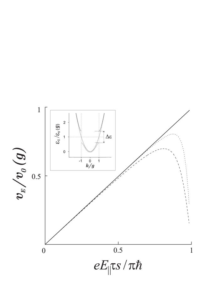
where is the electron subband number, is the unperturbed energy of an electron in a nanohelix in the absence of an external electric field, and is the characteristic energy of interaction of the electron with the electric field. The system of equations (4) clearly shows that a nanohelix in a transverse electric field represents a superlattice with the parameters controlled by the applied field . Particularly, the Bragg scattering of the charge carrier by the periodic potential (1) results in an energy gap opening at the edge of the superlattice Brillouin zone (see the inset to Fig. 1). It should be noted that the similar situation takes place in carbon nanotubes with helical crystal structure in the presence of a transverse electric field [4].
In what follows we will be mostly interested in the lowest branch of the energy spectrum. For weak enough electric fields, satisfying the condition , when solving the system of equations (4) for this branch, it is sufficient to take into account the admixture by the electric field of three electron states lowest in energy, neglecting the contribution of all other states. In this approximation the system of equations (4), which defines the electron energy spectrum, is reduced to just three equations, from which the dimensionless electron energy for the ground subband can be written within the first Brillouin zone as
| (5) |
where , , and
with . In the same approximation, the energy gap between the ground subband and the next one is given by
| (6) |
Superlattices based on semiconductor nanohelices can be used in electronic devices, which are currently based on conventional semiconductor superlattices, e.g., quantum cascade lasers [5], high-frequency generators and amplifiers [6], etc. The opportunity to control parameters of these devices by the applied electric field, , provides additional flexibility. As an example, let us consider a nanohelix-based superlattice subjected to an additional longitudinal electric field, , along the axis of the helix. We assume that in the absence of the longitudinal field the electron gas fills the states near the bottom of the ground subband. In the limit of weak longitudinal field, the typical change of the electron wave vector in the field, , is less than the width of superlattice Brillouin zone (here is the electron momentum relaxation time). Then the electric current in the nanohelix is , where is the electron density, and the drift velocity of electrons, , is described by the Esaki-Tsu formula [6]
| (7) |
Here is the electron velocity in the ground subband,
| (8) |
where is given by Eq. (5), and is the electron velocity at the edge of the superlattice Brillouin zone in the absence of the transverse electric field . From the drift velocity plot shown in Fig. 1 one can see that for and for high enough longitudinal electric fields, the electron drift velocity decreases with increasing electric field . This means the appearance of negative differential conductance with the threshold controlled by transverse electric field. This effect is caused by electron heating in the longitudinal electric field resulting in filling electron states with negative effective mass near the edge of the superlattice Brillouin zone. It should be noted that the further increase of electric field will result in the Zener tunneling breakdown of the energy gap (6), and the current will again increase with increasing . As a consequence, the current-voltage characteristic of a nanohelix will be of -type, which is similar to tunnel and Gunn diodes. In the same fashion as these diodes, the nanohelices might be used in amplifiers and generators.
The effect of negative effective mass near the edge of the superlattice Brillouin zone also leads to an efficient frequency multiplication in nanohelices. Let us consider an alternating electric field along the nanohelice axis, . Then the electric current in the nanohelix, as a function of time, can be written as the Fourier series
| (9) |
If , the coefficients in Eq. (9) are given by
| (10) |
From Eq. (8) it follows that the odd harmonics of the base frequency should appear in the response current. This effect can be used in frequency multipliers based on nanohelices.
In the case of weak scattering, when , the longitudinal electric field results in Bloch oscillations of electrons [6] with the frequency . For a typical nanohelix pitch of nm and electric field V/cm, the oscillation frequency c-1 lies in the terahertz range. This opens the possibility to use nanohelices [2] for resolving current challenges in terahertz optoelectronics [7].
This work is supported by the INTAS Foundation (Grant 05-1000008-7801), the Royal Society (UK), and the Russian Foundation for Basic Research (Grant 06-02-16005).
References
- [1] E.L. Ivchenko, G.E. Pikus, Superlattices and other heterostructures. Symmetry and optical phenomena (Springer-Verlag, Berlin, 1997).
- [2] V.Ya. Prinz, V.A. Seleznev, A.K. Gutakovsky, A.V. Chehovsky, V.V. Preobrazhenskii, M.A. Putiato, T.A. Gavrilova, Physica E 6 (2000) 828; V.Ya. Prinz, D. Grützmacher, A. Beyer, C. David, B. Ketterer, E. Deckardt, Nanotechnology 12 (2001) 399; V.Ya. Prinz, Phys. Stat. Sol. (b) 243 (2006) 3333.
- [3] I. Gradshteyn and I. Ryzhik, Table of Integrals, Series, and Products, edited by A. Jeffrey and D. Zwillinger (Elsevier, London, 2007).
- [4] O.V. Kibis, D.G.W. Parfitt, M.E. Portnoi, Phys. Rev. B 71 (2005) 035411; O.V. Kibis, S.V. Malevannyy, L. Huggett, D.G.W. Parfitt, M.E. Portnoi, Electromagnetics 25 (2005) 425.
- [5] J. Faist, F. Capasso, D.L. Sivco, C. Sirtori, A.L. Hutchinson, A.Y. Cho, Science 264 (1994) 553.
- [6] L. Esaki, R. Tsu, IBM J. Res. Dev. 14 (1970) 61.
- [7] M. Lee and M.C. Wanke, Science 316 (2007) 64; D. Dragoman, M. Dragoman, Progress in Quantum Electronics 28 (2004) 1; O.V. Kibis and M.E. Portnoi, Tech. Phys. Lett. 31 (2005) 671; E.A. Avrutin and M.E. Portnoi, Sov. Phys. Semicond. 22 (1988) 968; V.V. Kruglyak and M.E. Portnoi, Techn. Phys. Lett. 31 (2005) 1047.