e-mail esquin@physik.uni-leipzig.de, Phone +49-341-9732751, Fax +49-341-9732769
XXXX
Sample Size Effects on the Transport Characteristics of Mesoscopic Graphite Samples
Abstract
\abstcolIn this work we investigated correlations between the internal microstructure and sample size (lateral as well as thickness) of mesoscopic, tens of nanometer thick graphite (multigraphene) samples and the temperature and field dependence of their electrical resistivity . Low energy transmission electron microscopy reveals that the original highly oriented pyrolytic graphite material – from which the multigraphene samples were obtained by exfoliation – is composed of a stack of nm thick and micrometer long crystalline regions separated by interfaces running parallel to the graphene planes. We found a qualitative and quantitative change in the behavior of upon thickness of the multigraphene samples, indicating that their internal microstructure is important. The overall results indicate that the metallic-like behavior of at zero field measured for bulk graphite samples is not intrinsic of ideal graphite. The results suggest that the interfaces between crystalline regions may be responsible for the superconducting-like properties observed in graphite. Our transport measurements also show that reducing the sample lateral size as well as the length between voltage electrodes decreases the magnetoresistance, in agreement with recently published results. The magnetoresistance of the multigraphene samples shows a scaling of the form ( with a sample dependent exponent , which applies in the whole temperature 2 K K and magnetic field range T.
pacs:
81.05.Uw,73.21.-b,72.20.My1 Introduction
Ideal graphite consists on layers of honeycomb lattices of carbon atoms, characterized by two non-equivalent sites, A and B, in Bernal stacking configuration (ABABAB). Although there is not yet consent on the interlayer cohesive or binding energy per carbon atom between graphene layers in ideal graphite [2], several experimental facts suggest that this coupling is not larger than eV [3]. The huge anisotropy in the resistivity (ratio of the in-plane divided out-of-plane resistivities) at low and room temperatures, respectively, in good quality samples indicate the quasi two-dimensionality of the transport in the graphene layers of the graphite structure [3]. On the other hand, the effects of the real microstructure, the size and quality of the crystalline regions and their interfaces or even the influence of the overall sample size on the transport properties in single graphene, tens of graphene layers (multigraphene) as well as in bulk graphite samples are still not well studied.
A quick comparison between the published temperature () dependence of the resistivity at zero magnetic field () suggests that behaves differently in graphene and in high quality graphite. Whereas highly oriented pyrolytic graphite (HOPG) with narrow rocking curve widths shows a that decreases decreasing K, of single graphene layers appears to steadily increase decreasing , keeping the electron density low enough (see for example [4] and references inside). Although the influence of the substrates on the electronic transport of graphene is significant and cannot be neglected [5], the overall published experimental data do suggest that the ubiquitous decrease of (at K) appears only in good quality HOPG samples [6]. It is interesting to note that it remains still unclear, which is the absolute resistivity (parallel and perpendicular to the graphene planes) as well as the temperature dependence of defect free, ideal graphite. This is a basic question that still remains fully open due to the sensitivity of the graphite structure to defects. The results presented in these studies suggest that the resistivity of ideal graphite is not metal-like, i.e. decreases with in all the range.
Our work provides experimental hints on the correlations between the internal structure of the samples and their transport properties. The results are not only important to understand ideal graphite/graphene properties but also to understand the role of defects and/or interfaces within the graphite structure. Recently done high resolution magnetoresistance measurements on multigraphene samples show anomalous hysteresis loops below a “critical” temperature that indicates the existence of superconducting grains with high critical temperature embedded in a semiconducting matrix [7]. Those results are the last ones of a series of experimental hints suggesting the existence of granular superconductivity in graphite (for a short review see Ref. [8]). The data presented in this study provide a hint where these superconducting regions might be located.
Size effects
Recently published experimental work on highly oriented pyrolytic graphite (HOPG) showed that the change of the electrical resistance with magnetic field, i.e. the ordinary magnetoresistance (MR), decreases with the sample size even for samples hundreds of micrometer large [9]. This effect was ascribed to the large carrier mean free path as well as the large Fermi (or de Broglie) wavelength in graphite. Recently, García et al. [10] reported the development of an experimental method and its theoretical basis to obtain without free parameters these two transport properties based on the measurement of the resistance through micro-constrictions on a m thick HOPG sample. In that work micrometer large values for and at K were obtained in agreement with the expectations from the magnetoresistance results[9]. The carriers with the largest mean free path have m appear to be limited by the crystallite size in the used high quality HOPG sample [10].
In the last 50 years, the transport properties of graphite have been interpreted in terms of two- (three-) band Boltzmann-Drude approach[2]. However, the use of the standard approaches to understand the electrical properties of graphite is doubtful since due to the large carrier mean free path ballistic instead of diffusive transport should be applied. The large Fermi wavelength (due to the small carrier density of the carriers m) implies that diffraction effects within the sample may play also a role. Moreover, the differences in the transport properties between apparently similar samples together with electron force microscopy (EFM) results obtained on HOPG samples [11] provide further evidence that HOPG samples should be considered as a non-uniform electronic system. This non-uniformity is not an intrinsic property but it depends on parameters like the defect density or interfaces within the measured sample region and therefore we expect that the electrical resistance will depend on the measured sample size. The overall results presented in this study especially the sample size effects confirm once more the inadequacy of the standard models to understand the transport properties of graphite. All these results as well as the possibility that granular superconductivity could influence the transport of HOPG cast doubts on the applicability of the theoretical descriptions as has been done in the literature up to date to understand the transport properties of graphite.
Single graphene, multigraphene and the role of the microstructure
Nowadays there is a general interest of the solid state community on the transport properties of single graphite layers dubbed graphene [12]. As in the very first transport experiments done in graphene [13, 14], these samples are usually fixed on substrates. In general neither the possible variations of the electrical potential at the surface of the substrates as well as their shape variations nor the influence of the environment were considered important issues that may influence the transport properties of the graphene samples. Recent experimental evidence obtained in suspended graphene samples appears to confirm the detrimental effect of the substrates on the mobility of graphene [15, 16]. The lowest achievable electronic density (cm-2) in free standing as well as fixed-on-substrate graphene samples is still far away from the Dirac point, due to defects in the graphene structure, intrinsic bending or due to the influence of the substrate itself. This restriction limits the Fermi wavelength, , and therefore the largest achievable mobility () since the carrier mean free path cannot be larger than the size of the graphene samples. In fact, recently published work [5] showed that the minimum conductivity is governed not by the physics of the Dirac point singularity but rather by carrier-density inhomogeneities induced by the potential of charged impurities that may come from the substrate.
One possibility to overcome these limitations is to use several nanometers thick multigraphene samples, which are much less sensitive to the environment as well as to the substrates. In high quality graphite samples the graphene layers inside are of larger perfection than single graphene layers. Therefore it should be possible to obtain their intrinsic transport properties without external influence other than those coming from the lattice defects. A direct proof of the perfection of the graphene layers in high quality graphite is given by the very low carrier density measured at low temperatures, which is nearly two orders of magnitude smaller than the minimum obtained for suspended graphene samples [10].
In this work
we studied the temperature and magnetic field response of the electrical resistivity of multigraphene samples with thickness between 10 nm and 20m. Further characterization of the microstructure was done with a low voltage transmission electron microscope (TEM) that allowed us to observe some details of the internal structure of the samples as the typical distance between the interphases separating crystalline regions. Micro-Raman studies on some of the nanometer thick samples were also performed. We provide evidence for two size effects on the transport properties of multigraphene samples. One is related to the thickness and correlates to the internal microstructure of the samples. The second size effect deals with the influence of the sample lateral size on the transport properties. The paper has four more sections. Section 2 explains some details of the experimental methods we used. Section 3 describes the measured samples and their characteristics and includes the TEM and Raman results. Section 4 shows the main transport results. This section is divided in three subsections where we describe the different behavior of the transport properties upon the sample size. The main conclusions are given in Sec. 5
2 Experimental Details
Sample preparation
In order to carry out a systematic study we have performed measurements in different tens of nanometer thick multigraphene samples obtained by exfoliation from the same highly oriented pyrolytic sample with a mosaicity of (HOPG(0.4)). One part of the original HOPG sample was left with a thickness of m, which transport properties resemble the usual behavior observed in high-quality HOPG of similar characteristics [6].
The initial HOPG material of dimensions mm3 was glued on a substrate using GE 7031 varnish. We used a simple technique to produce the multigraphene films, which consists in a very carefully mechanical press and rubbing the initial material on a previously cleaned substrate. As substrate we used p-doped Si with a 150 nm SiN layer on top. This substrate helps to select the multigraphene films because – in comparison with Si substrates with a top layer of SiO2 – the SiN layer provides a higher color contrast allowing us to use optical microscopy to select the film. After the rubbing process we put three times the substrate containing the multigraphene films in a ultrasonic bath during 2 min using high concentrate acetone. This process cleans and helps to select only the good adhered multigraphene films on the substrate. After this process we used optical microscopy and later scanning electron microscopy (SEM) to select and mark the position of the films. For the production of the electrical contacts we used conventional electron lithography process. Afterwards the contacts were done by thermal deposition of Pd (99,95%) in high vacuum conditions. We have used Pd because it does not show any Schottky barrier when used with carbon. Measurements of the resistance of the Pd-electrodes alone showed negligible magnetoresistance. For the transport measurements the sample was glued on a chip carrier. The contacts from the chip carrier to the electrodes on the sample substrate were done using a m gold wire fixed with silver paste.
The advantage of using HOPG of good quality is that in these samples and due to the perfection of the graphene layers and low coupling between them, a low two-dimensional carrier density cmcm-2 in the temperature range 10 K K is obtained [10]. The carrier density values obtained in Ref. [10] are smaller than in typical few layer graphene (FLG) samples probably due to lattice defects generated by the used method to produce them and/or surface doping [15, 16].
Transport measurements
Low-noise four-wires (two for the input currents and two for the voltage measurement) resistance measurements have been performed by AC technique (Linear Research LR-700 Bridge with 8 channels LR-720 multiplexer) with ppm resolution and in some cases also with a DC technique (Keithley 2182 with 2001 Nanovoltmeter and Keithley 6221 current source). The temperature stability achieved was mK and the magnetic field, always applied normal to the graphene planes, was measured by a Hall sensor – just before and after measuring the resistance – and located at the same sample holder inside a superconducting-coil magneto-cryostat. We used current amplitudes between A. The measurement of the resistance at different positions of the same sample indicate that the contact resistance contributions in the absolute value as well as in the temperature and magnetic field measurements are negligible, as expected due to the four-wire configuration used. The magnetoresistance measurements were done always with the magnetic field applied perpendicular to the graphene planes, i.e. parallel to the samples c-axis.
Transmission Electron Microscopy
The images of the internal structure of the HOPG sample were obtained using a Nova NanoLab dual beam microscope from the FEI company (Eindhoven). A HOPG lamellae was prepared for transmission electron microscopy (TEM) using the in-situ lift out method of the microscope. The TEM lamellae of HOPG was cut perpendicular to the graphene layers. Therefore, the electron diffraction provided information on the crystalline regions and their defective parts parallel to the graphene layers. After final thinning, the sample was left on a TEM grid. A solid-state scanning transmission electron microscopy (STEM) detector for high-resolution analysis of thinned samples was used. The voltage applied to the electron column was 18 kV and the currents used were between 38 to 140 pA.
Micro-Raman Spectroscopy
Raman spectra of multigraphene samples were obtained at room temperature and ambient pressure with a Dilor XY 800 spectrometer at 514.53 nm wavelength (Green) and a m spot diameter. The incident power was varied between 0.5 to 3 mW to check for possible sample damage or laser induced heating effects. No damage and significant spectral change was observed in this range of incident power.
3 Samples Characteristics
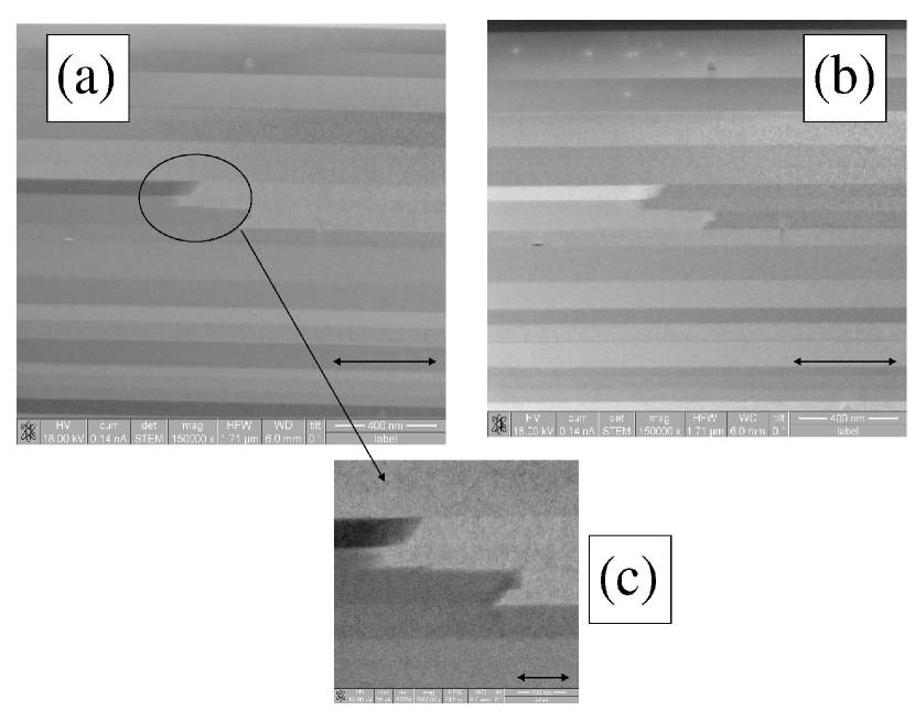
Table 1 shows the sample dimensions and names. The error bars in the thickness are the maximum estimated ones, taking into account the maximum error in the measurement and calibration of the optical and/or atomic force microscope (AFM) as well as the irregularities in the samples borders. The error in the absolute value of the resistivity takes those errors into account as well as errors in the width and length. Optical pictures of some of the measured samples are included in the figures below.
| Name | resistivity | thickness | length | width |
|---|---|---|---|---|
| Kcm] | ||||
| HOPG | m | 4.4 mm | 1.1 mm | |
| L5 | nm | m | m | |
| L8A | nm | m | m | |
| L2A | nm | m | m | |
| L8B | nm | m | m | |
| L7 | nm | m | m |
3.1 Transmission Electron Microscopy Results
Figure 1 shows the bright field (a) and dark field (b) details obtained with the low-voltage STEM. Figure 1(c) shows a blow out of a detail of (a). The different gray colors indicate crystalline regions with slightly different orientations. The images indicate that the average thickness of the crystalline regions is nm. One can also resolve the interfaces perpendicular to the c-axis of the layers and between the regions as well as the end parts of the crystalline regions along the graphene layers direction, see Fig. 1(c). Electron back scattering diffraction measurements done on similar HOPG samples indicate that the typical size of the single crystalline regions (on the (a,b) plane) ranges between 1 to m [10]. If the interface between the crystalline regions as well as the defects in the crystalline lattice have some influence on the transport properties we would expect to see a change in the behavior of the transport properties between samples of thickness of the order or less than the average thickness of the crystalline regions.
3.2 Raman Results
The Raman spectrum of graphite [17], a few layers and single graphene [18, 19] have been thoroughly measured and discussed in recent published studies and review. In this study we are interested in three Raman maxima, namely the G-peak around 1582 cm-1 due to a Raman active in-plane optical phonon E2g, its neighbor peak, the D-line around 1350 cm-1, which is very sensitive to the amount of lattice disorder, and the D’-line[18] (or 2D peak[19]) at cm-1 and its splitting in two or more maxima upon the number of graphene layers the sample has [18].
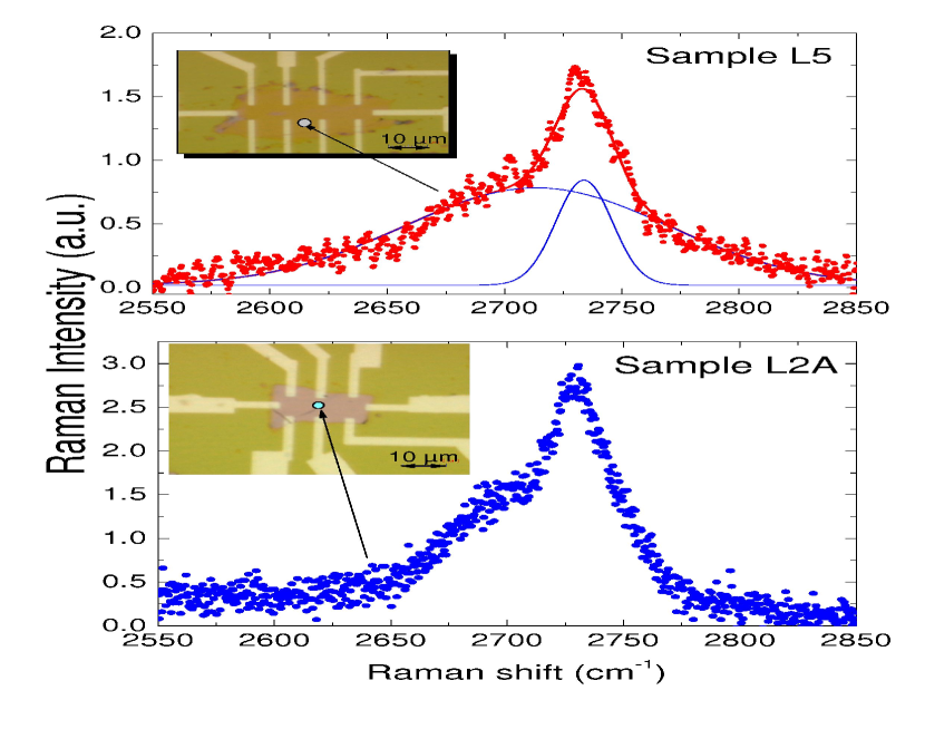
Figure 2 shows the Raman spectra of samples L5 (upper picture) and L2A (bottom) around the D’-line. The splitting into two peaks of the D’-line is in agreement with recently published results [18]. The main central narrow peak is at cm-1 whereas the value of the splitting is cm-1 in very good agreement with that observed for HOPG bulk. Taking into account that both samples L5 and L2A have a thickness between 10 and 20 nm, this difference in thickness does not affect the Raman D’-line. Taking this line as reference one would conclude that both samples are identical.
However, according to literature the structural quality of the samples can be resolved by investigating the D-line at cm-1. We note that also the edges of the samples as well as the borderlines between regions of different thicknesses may contribute to the D-band signal. The Raman spectra between 1300 and 1700 cm-1 have been measured at different positions of sample L5 and in sample L2A. The results are shown in Fig. 3 for the two samples. The broad D-line at cm-1 is clearly seen in sample L5 (at the same position as in Fig. 2) but it is completely absent in sample L2A. We checked that a similar curve is observed at different positions of the sample L5. The small peak at cm-1 in sample L2A is due to the substrate. The G line at cm-1 is observed for both samples, see Fig. 3. From these results we would conclude that sample L5 has more disorder or that the borders or edges have a larger influence to the Raman spectra than in sample L2A. From literature[20] we would expect that this disorder should have some influence on the transport properties of graphene as well as in a multigraphene sample.

4 Transport Measurements
4.1 Thickness and Temperature dependence of the resistivity at zero magnetic field
Figure 4 shows the resistivity at 4 K of the six measured samples vs. their thickness. It is clearly seen that the resistivity decreases increasing the sample thickness. The average change in resistivity between nm to m thick samples is about two orders of magnitude, far beyond geometrical errors. A similar behavior was observed recently in multigraphene samples obtained with a different, micromechanical method[21]. Because in that work no explicit absolute values of the resistivity at 4 K were given, we estimate it taking the in that work given mobility, assuming that the carrier density does not depend on the thickness and fixing arbitrarily the value of cm for the 12 nm thick sample reported in Ref. [21]. The open circles shown in Fig. 4 are the data points from Ref. [21]. A reasonable agreement between the two independently obtained measurements is obtained that speaks for the reproducibility of the observed dependence.

The authors in Ref. [21] suggested that the decrease of mobility (i.e. an increase in the resistivity at constant carrier density) decreasing sample thickness provides an evidence for boundary scattering. Taking into account the fact that one graphene layer shows finite mobility [15, 16], boundary scattering is certainly not the correct explanation for the observed behavior. A possible explanation for the observed trend is that the larger the thickness the larger is the amount of defects and interfaces in the sample, see Fig. 1, that produces the decrease in the resistivity. Since HOPG is a highly anisotropic material with huge anisotropy in the resistivity, it appears reasonable to assume that certain kind of lattice defects (vacancies, dislocations, etc.) may produce a sort of short circuits between layers, changing the dimensionality of the carrier transport and decreasing the resistivity. It appears unlikely, however, that randomly distributed point-like lattice defects can be the reason for the observed behavior. The results suggest the existence of a kind of thickness threshold around nm for the muligraphene samples obtained from HOPG(0.4) bulk graphite, see Fig. 5.
Regarding the two samples characterized with Raman we note that the sample L5, which shows a D-line (see Fig. 3) presumably due to the contribution of lattice disorder, has a lower resistivity than sample L2A that shows no D-line. In Ref. [20] was shown that extended defects in graphene can lead to self doping. Moreover, the presence of such defects can still lead to long carrier mean free path and a decrease in the resistivity. Our results speak for a non-simple influence of defects in graphite.
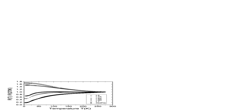
Figure 5 shows the normalized resistivity as a function of
temperature at zero magnetic field for all measured samples. The
overall results agree with those obtained for multigraphene samples
in Ref. [21]. However, we note the following, interesting
details:
- There is an apparent difference in the dependence between thick
and thinner samples. The samples thicker than nm show a
rather metallic behavior whereas thinner samples a semiconducting
like, see Fig. 5.
- There is basically no difference in the dependence between
sample L5 and L2A, with exception of the region at K where
decreases decreasing in the thicker sample L2A. This fact
indicates that the disorder the Raman D-line indicates does not
affect strongly the -dependence of the resistivity.
- The overall results indicate that the maximum at K in the
resistivity observed in sample L2A may have the same origin as the
decrease in the resistivity below K observed in thicker
samples, see Fig. 5. Taking into account the TEM results, see
Fig. 1, we would conclude that this metallic-like behavior is
not intrinsic to ideal, defect-free graphite or multigraphene but it
is due to the influence of the interfaces inside the samples with
large enough thickness.
The obtained results suggest that the true dependence of the resistivity in an ideal, defect-free multigraphene sample should be semiconducting-like, i.e. it should increase decreasing temperature. This dependence is actually the one expected for an ideal semimetal with zero or small energy gap, in agreement with the large decrease in carrier density decreasing temperature recently obtained in HOPG samples [10].
4.2 Magnetoresistance: Thickness dependence and scaling
The MR was measured for a few samples. Here we concentrate ourselves on two samples L5 and L7, see Fig. 5, which show a clear difference in the dependence of the resistivity. The results for these two samples are typical ones. The MR depends mostly on the behavior of the resistivity, i.e. whether it shows a semiconducting behavior like in samples L2, L2A (above 50 K) and L8A, or a metallic one, like in samples HOPG, L8B and L7.
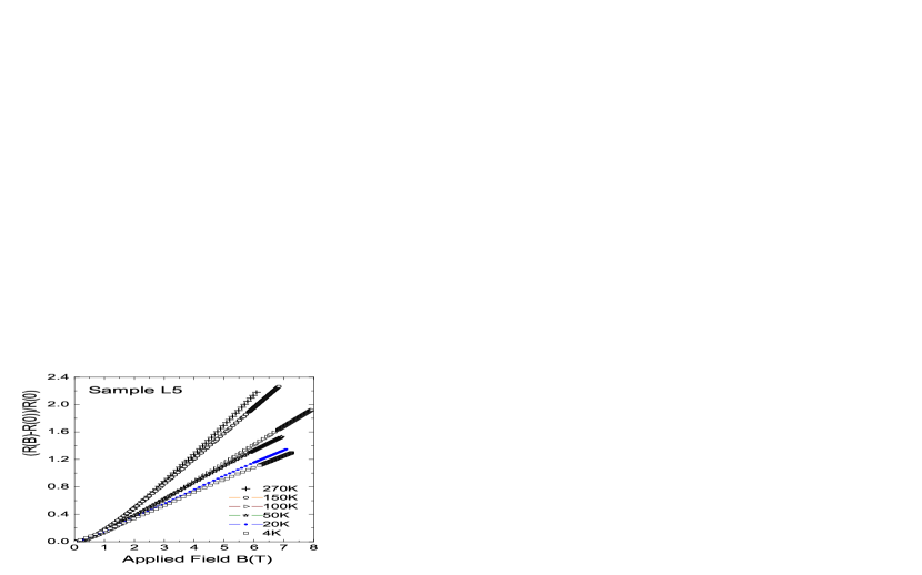
Figure 6 shows the MR vs. magnetic field defined as MR at different constant temperatures for sample L5. Above a field of T the MR increases with temperature. At lower fields it remains nearly independent. This increase of MR with , although anomalous, it is actually what one expects if the resistance decreases with , as is the case for sample L5. Note, however, that the MR is much weaker than the one measured in HOPG or Kish graphite bulk samples where the MR is larger than 1000 % at fields above 0.5 T and at low temperatures [6, 22, 23].
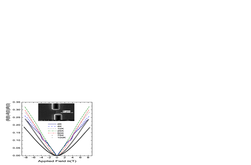
A qualitative and quantitative different behavior of the MR is obtained for the metallic-like sample L7, see Fig. 7. Here the MR decreases with temperature and it is a factor of larger than in the thinner sample L5. Because both samples have similar lateral sizes the difference in behavior in the MR should be related to the difference in thickness, i.e. in the number of interface regions within the sample that also may influence the resistivity. We show below that the MR can be related to the resistivity of each sample.
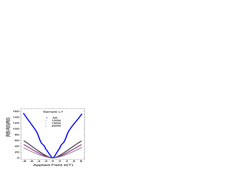
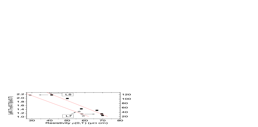
Figure 8 shows the MR for both samples L5 and L7 at 6 T field at different temperatures as a function of the resistivity at the same temperatures. This figure shows that the decrease or increase of the MR with is related to the resistivity value at zero field. This result appears to be compatible with the semi classical picture for the magnetoresistance, i.e. the longer the relaxation time – or the smaller the resistivity – the larger can be the effect of the field on the resistance.
As shown in Fig. 8 the MR of multigraphene samples as
well as in HOPG bulk samples [24] does not follow the well
known Kohler’s rule. This rule describes the MR as a functional
scaling with the ratio , i.e. in lowest order the MR . There are at least three different reasons for the
failing of the Kohler rule in graphite, namely:
- One reason is related to the huge electron mean free path
in graphite, which is much larger than the radius of curvature of an
electron orbit under a magnetic field , with the effective electron mass, m/s the
Fermi velocity and the electron charge. For a field of 1 T, for
example, we have m whereas m for K at zero field [10].
- Other reason is that the semiclassical picture of the MR breaks
down when the Fermi wavelength gets larger than ,
i.e. what is the meaning of the classical cyclotron radius m at T when the wavelength of the electrons
m below 200 K [10].
- A third effect might be related to the contribution of the sample
internal structure and interfaces. These defects may not only
influence the dimensionality of the transport in graphite (short
circuiting the graphene planes) but also might be the origin for
localized, granular superconducting regions. Recently done study of
the behavior of the MR of multigraphene samples suggests the
existence of granular superconductivity [7]. The main
experimental evidence comes from the anomalous irreversible behavior
of the MR, which appears compatible with Josephson-coupled
superconducting grains [7].
We note that Bi, as graphite, has a low density, low effective mass of carriers and huge values of the electron mean free path [25, 26]. It shows a very similar magnetic field induced metal-insulator transition and also has a very low resistivity [22]. We may speculate that a similar superconductivity phenomenon may play a role. In fact recently published work found that crystalline interfaces in Bi bicrystals of inclination type show superconductivity up to 21 K [27, 28]. A similar situation may occur at the interfaces between crystalline regions in oriented graphite, see Fig. 1.
An important point we would like to stress here is that the peculiar behavior of the MR in HOPG samples [6] is observed only for fields applied perpendicular to the graphene layers. For fields parallel to the graphene layers there is no MR, i.e. the measured very weak MR can be explained by the misalignment of the field with respect to the graphene planes [29]. This speaks for a huge anisotropy of the assumed superconducting region. Therefore the available experimental data suggest the interface regions as possible candidates where this superconductivity might be located, see Fig. 1. Within the same schema it appears clear that the decrease or even the level-off of the resistivity decreasing temperature, see Fig. 5, would not be intrinsic but due to the influence of the interface regions.
In case we have non-percolative superconducting arrays of grains, one would expect to have a relatively larger increase in the resistance with magnetic field mostly in the temperature region where the influence of the coupling between superconducting grains at no applied field is observable, i.e. in a region where either the resistance decreases decreasing temperature or it levels off below a certain temperature as for samples L5 and L8A below 25 K or below 30 K for sample L2A, see Fig. 5. This is expected for granular superconductors due to a coherent charge transfer of fluctuating Cooper pairs between the grains [30]. This sensitive change of the temperature dependence of the resistance under an applied magnetic field has been already seen in Ref. [31] for bulk HOPG samples. The possibility of superconductivity in graphite has been discussed in recent years, see Refs. [8, 7] for further reading.
On the other hand, in a multigraphene sample we certainly have other defects that would not trigger local superconductivity but increase the carrier density, decreasing and therefore for a large enough sample (see section 4.3) the MR should increase. Simultaneously, reducing the Schubnikov-de Haas (SdH) oscillations in the MR should be recovered, as seen in sample L7 at low temperatures and high fields, see Fig. 7. This is similar to the effect observed in graphene layers by applying a large enough bias voltage, increasing the carrier density, decreasing and recovering the SdH oscillations [13].
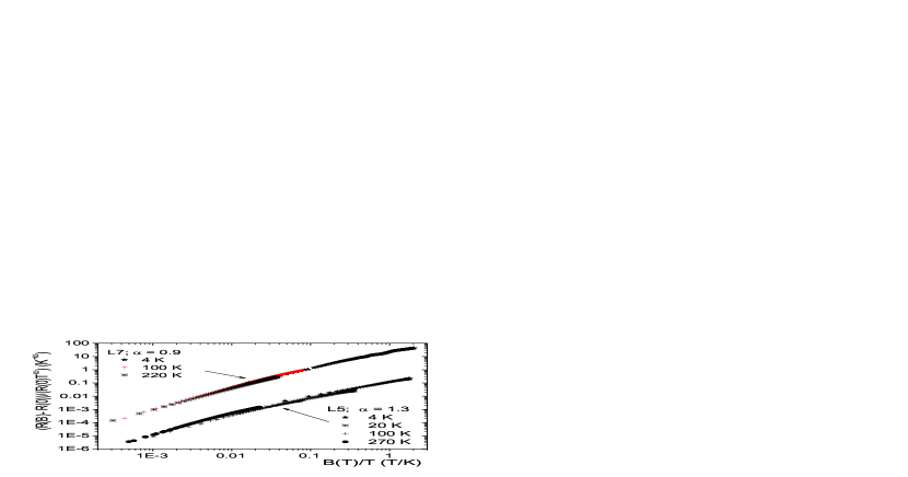
Finally, we would like to remark an interesting aspect of the MR related to its field and temperature dependence. The field dependence of the MR is quasi-linear in field at low enough temperatures and high enough fields T), see for example the MR for sample L5 in Fig. 6. This behavior is still not well understood; possible explanations are based on Landau level quantization of the Dirac fermions [32] or due to the circulations of quantum, inhomogeneous current paths at the borders of graphite platelets creating a Hall-like voltage contribution to the MR [33]. As mentioned above, neither the MR of the multigraphene samples studied in this work nor the one in bulk graphite follows the classical Kohler scaling. We have found however, that the MR data for the multigraphene samples L5 and L7 show an impressive scaling when is plotted vs. the ratio , as can be seen in Fig. 9 for and , respectively.
This kind of universal scaling of the magnetoresistance has been observed previously in different materials near a metal-insulator transition, like in metallic Si:B () [34], icosahedral AlPdRe () [35] or in intercalated amorphous carbon () [36]. Whereas the scaling with has a physical interpretation based on electron-electron interactions [34], deviations from this value remain unexplained. The scaling obtained for samples L5 and L7 is indeed extraordinary since it covers several orders of magnitude in both scaled axes and appears to be unique in the literature. Future studies should clarify whether this scaling is related to the influence of superconductivity in the MR.
4.3 Lateral Size dependence of the Magnetoresistance
As has been shown in recent work on HOPG bulk samples[9] the lateral size of the sample has an influence on the MR. This can be qualitatively understood if we take into account that: (a) The de-Broglie wavelength for massless Dirac fermions (m/s is the Fermi velocity and a typical Fermi energy K) or for massive carriers with effective mass , , as well as the Fermi wavelength can be of the order of microns or larger due to the low density of Dirac and massive fermions. (b) Due to the extraordinary large values of the mean free path of the carriers in bulk HOPG () mm [10], at low enough temperatures we expect to see a decrease of the MR reducing the lateral sample size or the distance between the voltage electrodes.
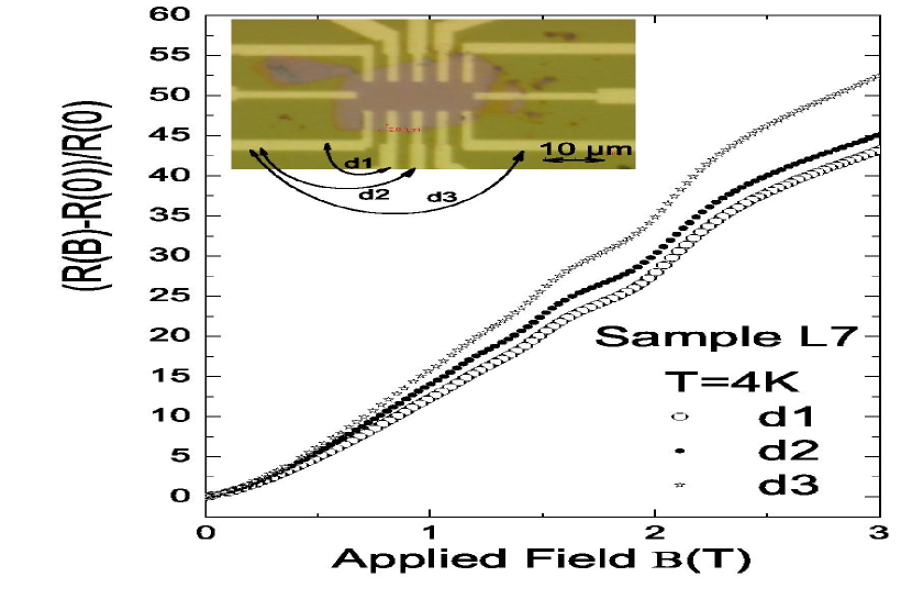
Figure 10 shows the MR of sample L7 measured at three different voltage electrode positions d1, d2 and d3, see inset. As expected, the larger the distance between voltage electrodes the larger the MR. Note that a clear effect is observed changing the distance from to 16 m indicating that the mean free path should be of this order, in agreement with recently published results [10].
The lateral size effect on the MR is also nicely observed in bulk HOPG samples with a constriction. Using the Ga+-ion beam of the DBM we have prepared a m wide constriction at the middle and between the sample electrodes, see inset in Fig. 11 where the results for the MR at different temperatures are shown. The MR of the HOPG sample with a constriction is about two orders of magnitude smaller than in the original sample. Leaving by side the influence of the SdH oscillations we note that the MR at T remains nearly -independent from 4 K to 25 K and decreases at higher temperatures. We note also that at zero field the ratio between the resistivities at 50 K and 4 K for the sample with constriction, see Fig. 11, whereas it is for the original sample, see Fig. 5. Therefore, the behavior of the MR can be understood assuming that the mean free path remains larger than the width of the constriction at K and is smaller at higher . This lateral size effect on the MR indicates that the effective mean free path of the carriers responsible for the MR should be of the order of m at K, in excellent agreement with recently reported values for similar HOPG samples [10]. In case granular superconductivity is confirmed in oriented graphite, future studies should clarify to which extent this phenomenon contributes to the observed lateral size effect in the MR.
5 Conclusion
The data obtained in this investigation imply that multigraphene samples show two size effects. The smaller the thickness of the multigraphene sample the larger is the resistivity. The correlation between the thickness dependence of the resistivity and the microstructure of highly oriented pyrolytic graphite suggests that the interfaces between crystalline regions and parallel to the graphene layers could be the regions where granular superconductivity is located. The differences of the temperature as well as the magnetic field dependence of the resistivity of different multigraphene samples suggest that those interfaces play a main role. The available data indicate that the intrinsic -dependence of the resistivity of ideal multigraphene or graphite would be semiconducting-like. This would imply that interpretations based on the metal-like transport properties of graphite as well as multigraphene samples should not be related to the properties of an ideal graphite structure. The lateral size dependence of the transport properties, specially in the magnetoresistance, can be understood taking into account the large effective mean free path of the carriers.
It is a pleasure to thank Dr. S. Reyntjens from the FEI company in Eindhoven for providing us with the TEM images of the HOPG sample. Fruitful discussions with N. García are gratefully acknowledge. We gratefully thank U. Teschner and W. Grill for the Raman measurements. This work was supported by the DFG under DFG ES 86/16-1. J.-L. Yao acknowledges the support of the A. v. H. Foundation and J. B-Q. the support of the EU project “Ferrocarbon”.
References
- [1]
- [2] B. T. Kelly, Physics of Graphite (London: Applied Science Publishers, 1981).
- [3] Y. Kopelevich and P. Esquinazi, Adv. Mater. (Weinheim, Ger.) 19, 4559 (2007).
- [4] Y. W. Tan, Y. Zhang, H. Stormer, and P. Kim, Eur. Phys. J. Special Topics 148, 15–18 (2007).
- [5] J. H. Chen, C. Janga, S. Adam, M. S. Fuhrer, E. D. Williams, and M. Ishigam, Nature Physics 4, 377–381 (2008).
- [6] Y. Kopelevich, P. Esquinazi, J. H. S. Torres, R. R. da Silva, and H. Kempa, Advances in Solid State Physics, B. Kramer (Ed.), Vol. 43, (Springer-Verlag Berlin, 2003), pp. 207–222.
- [7] P. Esquinazi, N. García, J. Barzola-Quiquia, M. Muñoz, P. Rödiger, K. Schindler, J. L. Yao, and M. Ziese, arXiv:0711.3542.
- [8] Y. Kopelevich and P. Esquinazi, J. Low Temp. Phys. 146, 629–639 (2007), and refs. therein.
- [9] J. C. González, M. Muñoz, N. García, J. Barzola-Quiquia, D. Spoddig, K. Schindler, and P. Esquinazi, Phys. Rev. Lett. 99, 216601 (2007).
- [10] N. García, P. Esquinazi, J. Barzola-Quiquia, B. Ming, and D. Spoddig, Phys. Rev. B 78, 035413 (2008).
- [11] Y. Lu, M. Muñoz, C. S. Steplecaru, C. Hao, M. Bai, N. García, K. Schindler, and P. Esquinazi, Phys. Rev. Lett. 97, 076805 (2006), see also the comment by S. Sadewasser and Th. Glatzel, Phys. Rev. lett. 98, 269701 (2007) and the reply by Lu et al., idem 98, 269702 (2007); D. Martinez-Martin and J. Gomez-Herrero, arXiv:0708.2994 (unpublished); R. Proksch, Appl. Phys. Lett. 89, 113121 (2006).
- [12] M. I. Katsnelson, Materialstoday 10, 20 (2007).
- [13] K. S. Novoselov, A. K. Geim, S. V. Morozov, S. V. Dubonos, Y. Zhang, and D. Jiang, Nature 438, 197 (2005).
- [14] Y. Zhang, Y. W. Tan, H. Störmer, and P. Kim, Nature 438, 201 (2005).
- [15] K. I. Bolotin, K. J. Sikes, Z. Jiang, M. Klima, G. Fudenberg, J. Hone, P. Kim, and H. L. Stormer, Solid State Commun. 146, 351 (2008).
- [16] X. Du, I. Skachko, A. Barker, and E. Y. Andrei, arXiv:0802.2933.
- [17] S. Reich and C. Thomsen, Philos. Trans. R. Soc. London, Ser. A 362, 2271 (2004).
- [18] D. Graf, F. Molitor, K. Ensslin, C. Stampfer, A. Jungen, C. Hierold, and L. Wirtz, Nano Lett. 7, 238–242 (2006).
- [19] A. C. Ferrari, J. C. Meyer, V. Scardaci, C. Casiraghi, M. Lazzeri, F. Mauri, S. Piscanec, D. Jiang, K. S. Novoselov, S. Roth, and A. K. Geim, Phys. Rev. Lett. 97, 187401 (2006).
- [20] N. M. R. Peres, F. Guinea, and A. H. C. Neto, Phys. Rev. B 73, 125411 (2006).
- [21] Y. Zhang, J. P. Small, W. V. Pontius, and P. Kim, Appl. Phys. Lett. 86, 073104 (2005).
- [22] X. Du, S. W. Tsai, D. L. Maslov, and A. F. Hebard, Phys. Rev. Lett. 94, 166601 (2005).
- [23] T. Tokumoto, E. Jobiliong, E. Choi, Y. Oshima, and J. Brooks, Solid State Commun. 129, 599 (2004).
- [24] H. Kempa, P. Esquinazi, and Y. Kopelevich, Phys. Rev. B 65, 241101(R) (2002).
- [25] A. N. Friedman, Phys. Rev. 159, 553 (1967).
- [26] V. F. Gantmakher and Y. S. Leonovov, JETP Letters 8, 162 (1968).
- [27] F. Muntyanua, A. Gilewski, K. Nenkov, J. Warchulska, and A. Zaleski, Phys. Rev. B 73, 132507 (2006).
- [28] F. Muntyanua, A. Gilewski, K. Nenkov, A. Zaleski, and V. Chistol, Solid State Commun. 147, 183–185 (2008).
- [29] H. Kempa, H. C. Semmelhack, P. Esquinazi, and Y. Kopelevich, Solid State Commun. 125, 1–5 (2003).
- [30] I. V. Lerner, A. A. Varlamov, and V. M. Vinokur, Phys. Rev. Lett. 100, 117003 (2008).
- [31] Y. Kopelevich, V. Lemanov, S. Moehlecke, and J. Torres, Phys. Solid State 41, 1959–1962 (1999).
- [32] A. A. Abrikosov, Europhys. Lett. 49, 789 (2000).
- [33] H. Kempa, P. Esquinazi, and Y. Kopelevich, Solid State Communication 138, 118–122 (2006).
- [34] S. Bogdanovich, P. Dai, M. P. Sarachik, and V. Dobrosavljevic, Phys. Rev. Lett. 74, 2543–2546 (1995).
- [35] V. Srinivas, M. Rodmar, R. König, S. J. Poon, and O. Rapp, Phys. Rev. B 65, 094206–1–8 (2002).
- [36] L. Kumari and S. V. Subramanyam, Mater. Sci. and Eng. B 129, 48–53 (2006).