Compact cryogenic Kerr microscope for time-resolved studies
of electron spin transport in
microstructures
Abstract
A compact cryogenic Kerr microscope for operation in the small volume of high-field magnets is described. It is suited for measurements both in Voigt and Faraday configuration. Coupled with a pulsed laser source, the microscope is used to measure the time-resolved Kerr rotation response of semiconductor microstructures with 1 micron spatial resolution. The microscope was designed to study spin transport, a critical issue in the field of spintronics. It is thus possible to generate spin polarization at a given location on a microstructure and probe it at a different location. The operation of the microscope is demonstrated by time-resolved measurements of micrometer distance diffusion of spin polarized electrons in a GaAs/AlGaAs heterojunction quantum well at 4.2 K and 7 Tesla.
I Introduction
The field of spintronics aims at manipulating the spin and charge degrees of freedom of carriers in order to expand the functionalities of current electronic devices. In this field, microscopy based on the magneto-optical Kerr effect (Kerr microscopy) is particularly valuable for measuring spin polarization in ferromagnetic and semiconductor micro and nanostructures. In recent years, Kerr microscopy has been applied by several research groups to study phenomena relevant to spintronics. For example, Awschalom and coworkers utilized a room-temperature optical microscope, electromagnet and cryogenic cell with cold finger to measure continuous-wave (cw) and time-resolved Kerr rotation in biased semiconductor strips Kikkawa99 . Erskine and coworkers studied room-temperature domain wall propagation in permalloy nanowires subject to fast-rise time magnetic field step waveforms utilizing an oblique-incidence Kerr polarimeter with 2 m spatial resolution and 1 ns temporal resolution Beach05 ; Nistor06 . Imamoğlu and coworkers utilized a bath cryostat with superconducting magnet that incorporated optics, detectors and positioners inside the cryostat for cw measurements of single spins in quantum dots Atature07 .
Characteristics that are desirable in a Kerr microscope for spintronics research are the ability to apply large magnetic fields, a time-resolution on the timescale of the spin dynamics, the ability to excite and probe spins at different locations using different photon energies and the possibility to operate in Voigt and Faraday geometries. Application of large magnetic fields is often desirable in order to produce large Zeeman splittings or to distinguish between different spin populations in a sample. Time-resolving spin dynamics has proven to be a very powerful tool in the field of spintronics. It allows direct observation of spin precession, dephasing and transport. Studies of spin transport, in particular, benefit from the ability of exciting spin polarized carriers in one place and detecting them at a different location. The possibility to operate the microscope while applying the magnetic field parallel to the sample plane (Voigt configuration) or perpendicular to the sample plane (Faraday configuration) allows, for example, controlling the magnetization orientation of ferromagnetic films with perpendicular or in-plane magnetic anisotropy. Moreover, in band-gap engineered semiconductor heterostructures, two-dimensional charge carrier systems can be Zeeman- or Landau split in these configurations, respectively. This can be exploited, for example, in dilute magnetic semiconductors like GaN:Gd Lo08 .
Additional characteristics that are desirable in the Kerr microscope are high sensitivity, high spatial resolution and possibility of cryogenic operation. The sensitivity of the Kerr microscope is given by the minimum Kerr rotation angle that can be measured and is typically of the order of a few rad. High spatial resolution can be achieved with objective lenses of very short focal distance. The spatial resolution r is determined by the wavelength of the laser source utilized and the numerical aperture of the objective lens NA:
| (1) |
Submicrometer resolution is easily achievable using high-NA objective lenses (NA 1) and laser sources with wavelengths in the UV, visible or near IR range. However, in practice, the small cryogenic measurement volumes inside high-field magnets enforce long distances between room temperature optics and the sample. This is in conflict with the convenience of utilizing high-quality microscope objectives at room temperature. The possibility of cryogenic operation is important, among other reasons, because spin relaxation rates tend to be strongly temperature dependent. This temperature dependence often helps identifying the dominant spin relaxation mechanism.
In this article a cryogenic sample-scanning Kerr microscope for static and time-resolved Kerr rotation (TRKR) measurements in high magnetic fields is described. A compact design based on in situ operation of an aspherical singlet lens and a piezo-driven translation stage allows obtaining micron-scale resolution inside the bore of a large superconducting magnet. The instrument can operate in Faraday and Voigt configurations and with femtosecond or cw lasers. The spatial resolution can be as good as 1 micrometer. Sample temperature can be set between 1.5 K and 300 K and magnetic fields of up to 8 Tesla can be applied. The capabilities of the microscope are demonstrated by measuring the time-resolved Kerr rotation response of devices fabricated on a GaAs/AlGaAs heterojunction quantum well at 4.2 K and 7 Tesla. The applicability of the instrument for time-resolved studies of spin transport is demonstrated by measuring micrometer distance diffusion of spins precessing in an applied magnetic field.
II Instrument configuration
The Kerr microscope consists of three main parts: 1. light source, tabletop optics and detection system, 2. magneto-optical cryostat and 3. insert which contains an XYZ sample positioner, objective lens and electrical leads to the sample. Figure 1 shows a schematic of the most important components of the system. In this section the configuration of the three parts of the microscope will be discussed in detail, focusing on the configuration required for time-resolved Kerr rotation measurements of spin transport in semiconductor microstructures in the Voigt geometry. Data taken in this configuration will be presented. The possibility of changing to other configurations, for example to Faraday geometry or static Kerr measurements, do not present major difficulties.
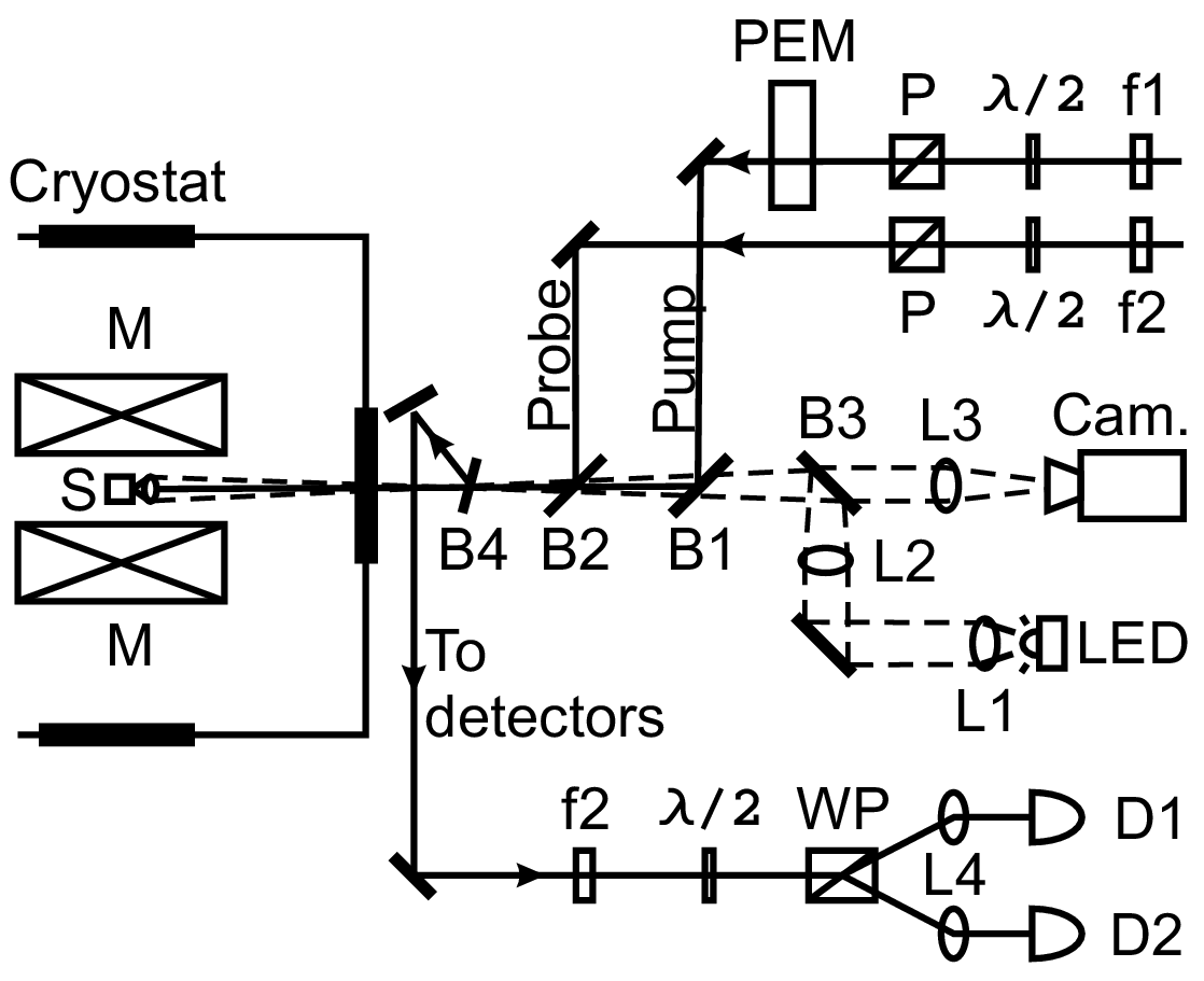
The light source, tabletop optics and detection system generate and deliver the appropriate light beams to the sample and detect the changes of polarization of the reflected beam. For time-resolved Kerr rotation measurements, a pulsed laser system is utilized. In this case two light pulses are required: a pump pulse which generates a non-equilibrium spin polarization in the sample and a probe pulse which measures this non-equilibrium spin polarization at a certain location and at a different moment in time. Light pulses are generated by a cavity-dumped Ti:sapphire laser (KMLabs Inc. Cascade) with pulse width of 20 fs. The laser spectrum is centered at 800 nm and has a full-width at half-maximum (FWHM) of 80 nm. A prism compressor is used to pre-compensate for dispersion caused by several millimeters of calcite and quartz in the beam path before the sample. A 1:5 beamsplitter is used to divide the single beam from the laser source into separate pump and probe beams. The time delay between the pump and probe pulses can be set by a computer-controlled delay stage (Physik Instrumente M-531.DD) with 0.1 micron step size and travel range of 60 cm. Half-wave plates ( in Fig. 1) followed by Glan-Thomson polarizers (P) in both pump and probe arms are used to produce beams with well defined polarization. A photoelastic modulator (Hinds PEM-90 I/FS50) placed on the path of the pump beam modulates its polarization between right-circular polarization and left-circular polarization at a frequency of 50 kHz. In order to study the laser wavelength dependence of the Kerr response of the sample, 10 nm (18 meV) FWHM spectral bandwidth interference filters are placed in the path of both pump (f1) and probe beams (f2). The resulting spectral filtering increases the width of both pulses to approximately 120 fs. The measurements that will be discussed in the following section were done utilizing filters centered at 780 nm for the pump and 820 nm for the probe beams.
In order to control the positions of pump and probe beams on the sample and their separation, imaging and beam steering optics were installed. A near-IR sensitive camera (JAI CV-M50IR) is used for imaging (Cam. in Fig. 1). Both imaging and illumination are done through the objective lens in the microscope insert (detail description of the microscope insert is given below). The sample is illuminated using a collector lens (L1, focal length 4 cm) which collimates the light from a white light-emitting diode and a condenser lens (L2, focal length 15 cm) which focuses this light a few centimeters in front of the objective lens in the insert. The objective lens focuses the white light illuminating an area on the sample of approximately 150 microns in diameter. Light reflected from the sample is collected by the objective lens and is focused onto the camera using a large diameter achromatic lens with focal length 19 cm (L3). The pump and probe beams incident on the sample are also imaged by the camera allowing easy beam steering. The position of pump and probe beams on the sample is manually controlled by steering beamsplitters B1 and B2 using high-resolution actuators. The angular sensitivity achievable in this configuration is approx. 4.6 arcsecond. The effective focal length of the objective lens is 2.75 mm, which gives a lateral beam displacement sensitivity of 0.06 microns.
The detection system consists of a balanced photodiode bridge which measures the rotation of the plane of polarization of the reflected probe beam. The probe light reflected from the sample is collected and collimated by the objective lens in the insert after which the light is sent to the detection system by beamsplitter B4 indicated in Fig. 1. An interference filter, f2 in the figure, similar to the one in the probe beam path, is used to reject the pump light. A half-wave plate rotates the probe polarization by 45∘ after which the probe is split into two beams with s- and p-polarizations using a Wollaston prism (WP). The emerging beams are detected by separate but identical photodiodes D1 and D2. Voltage outputs from the photodiodes are subtracted and sent to a lock-in amplifier. The voltage measured by the lock-in amplifier at the frequency of the polarization modulation (50 kHz) is, to first order, proportional to the Kerr rotation angle. Kerr ellipticity contributes to the measured voltage only as a third order correction. In order to balance the photodiode bridge, the half-waveplate before the Wollaston prism is rotated slightly until the difference between the signals measured with the two photodiodes is minimum. A rotation of the plane of polarization of the probe beam caused by the pump pulse causes an increase in the intensity detected by one of the photodiodes and a decrease in the intensity detected by the other. The difference between the two intensities can be positive or negative, indicating Kerr rotation angles of opposite signs.
A magneto-optical cryostat is used to control the sample temperature and to apply a static magnetic field. The cryostat used was an Oxford Instruments Spectromag SM4000-8 equipped with a split pair superconducting split-coil magnet (M in Fig. 1) capable of producing magnetic fields of up to 8 Tesla. The sample is cooled by He gas flow from a liquid He reservoir. Sample temperature can be set between 1.5 K and 300 K. The split pair magnet allows optical access to the sample with the magnetic field applied along the optical axis (Faraday configuration) or perpendicular to it (Voigt configuration). The orientation of the magnetic field can be changed by 180∘ without modifying the optics by use of the bipolar power supply of the magnet.
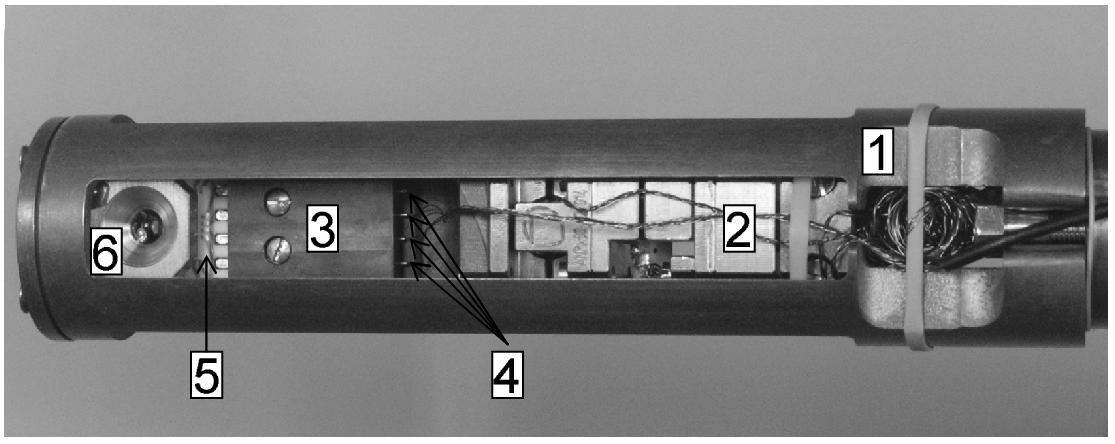
The sample insert is the most critical part of the Kerr microscope. It contains the sample, objective lens, temperature sensor, sample positioning and focusing system and electrical leads to the sample. The insert is placed inside the magneto-optical cryostat, requiring all parts to perform well at low temperatures and high magnetic fields. A picture of the insert with all parts indicated is shown in Fig. 2. The insert consists of a cylindrical copper housing fixed at the end of the sample rod supplied with the magneto-optical cryostat. The cylinder diameter is 25 mm. The objective lens is mounted on a copper/polyimide holder at the bottom of the copper cylinder. The special lens holder ensures that no stress is applied to the lens due to thermal contraction of the materials during cool down. The objective lens will be discussed in more detail later. The sample is mounted on a modified ceramic chip carrier with eight electrical lead contacts and placed approximately in the focal plane of the objective lens. The chip carrier is mounted on an all-polyimide frame. The frame material was chosen to have low thermal contraction and good electrical isolation properties. Eight spring-loaded pins mounted on the frame make electrical contact with the leads in the chip carrier. In addition, the spring force of the pins holds the chip carrier in a fixed position in the polyimide frame and allows changing the samples easily by simply placing a different chip carrier into the frame. A Cernox temperature sensor (LakeShore CX-1050-SD, not visible in the figure) is placed on the frame in order to accurately monitor the temperature of the sample.
The polyimide frame holding the sample is screwed onto an XYZ inertial piezo-driven translation stage (Attocube Systems ANPxyz50/LT) having 10 nm minimum step size at 4.2 K and a total travel range of 4 mm in the x and y directions and 3 mm in the vertical direction. The small step size of the translation stage allows accurate scanning and positioning of microstructures with respect to the focused laser beams while its long travel range allows measuring several devices on a single sampleMeyer05 . After each step of the translation stage, the piezos go back to zero voltage resulting in no drift of the sample position due to noise in the piezo driving electronics. The translation stage holding the polyimide frame and chip carrier is fixed inside of the copper cylinder on the top part. This allows free displacement of the sample with respect to the objective lens. Translating the sample along the optical axis of the objective lens changes the focusing of the laser beam as well as the focusing of the image of the device surface captured by the camera. Translation in the remaining two directions allows scanning the sample surface.
Proper selection of the objective lens in the insert is decisive to the performance of the microscope. Since the microscope is designed to work with a split-pair magnet both in Faraday and Voigt configurations, space constrains inhibit the use of mulit-element microscope objectives. Instead, a single, high-numerical aperture aspherical lens has to be used.
Diffraction-limited focusing of the incoming laser beams ensures the highest spatial resolution. Spherical and chromatic aberrations are major obstacles in obtaining a diffraction-limited spot size on the optical axis of the objective lens. For measurements of spin transport it is necessary to ensure nearly diffraction-limited spots not only on-axis but also off-axis. In this case it is essential to minimize comatic aberration.
The detrimental effects of spherical aberration can be minimized by utilizing specially designed aspheric lenses. A wide range of small diameter high-NA aspheric lenses designed for wavelengths in the vicinity of 800 nm are commercially available. In order to choose the proper lens for the Kerr microscope geometrical ray tracing calculations of selected aspheric lenses were performed. Incoming parallel rays, both marginal and paraxial, were traced through the lenses at different wavelengths within the laser spectrum. Subsequently the diameter of the focal spot for each lens was calculated when focusing the beams on-axis and off-axis. The parameters that entered the calculation are the known refractive index values of the lens material, the incoming light wavelengths and the aspheric coefficients for both lens surfaces. A detailed comparison was made for two aspheric lenses designed for 830 nm with numerical aperture 0.68, one biconvex (LightPath 350330) and one plano-convex (LightPath 350390). The calculations revealed that with the biconvex lens on-axis diffraction-limited spot size can be achieved at the design wavelength (spherical aberration-free). In contrast, the plano-convex lens causes some spherical aberration even at the design wavelength. Plano-convex lenses, however, have minimum comatic and spherical aberrations when focusing a collimated beam. In fact, comatic aberration of the biconvex lens was calculated to be much larger than that of the plano-convex lens. By taking this into account the plano-convex lens was chosen to be most appropriate for the Kerr microscope. According to our calculations for the plano-convex lens, the combined spherical and chromatic aberrations (for 10 nm spectral bandwidth) increase the diameter of the on-axis spot by only 6 compared to the diffraction-limited case.
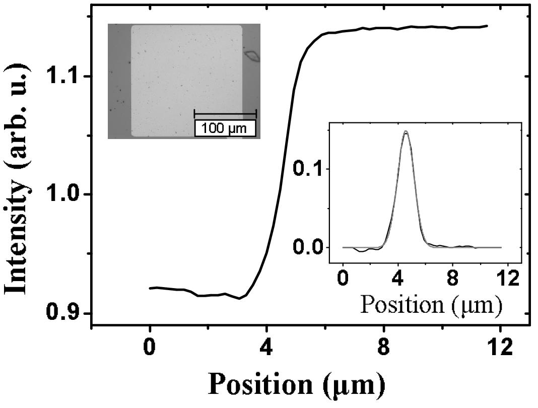
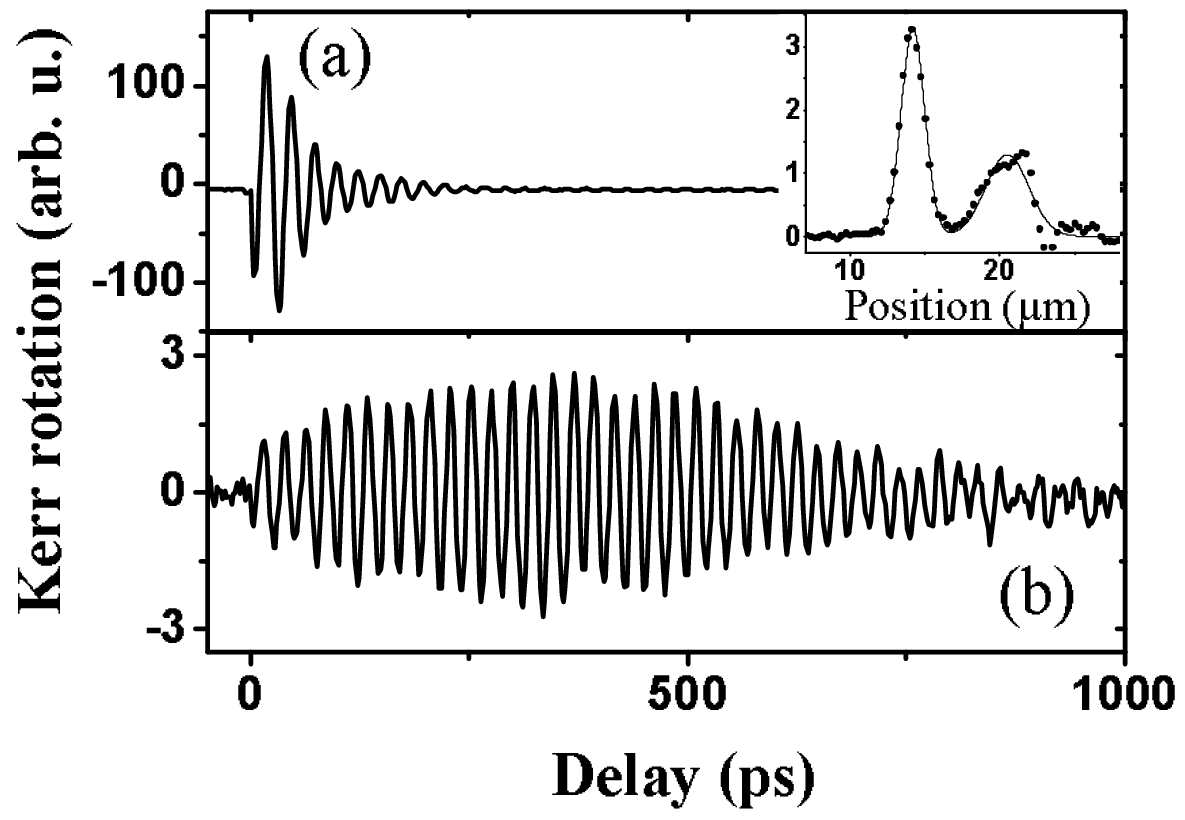
Spatial profiles of the laser light at the focus are measured with a knife-edge technique. The laser beam is focused on the surface of the sample, in this case, an epitaxially grown GaAs/AlGaAs heterojunction structure. A square Ti/Au pad (170 m wide and 150 nm thick) was deposited on the sample surface by lithography and lift-off (see the inset on the top-left corner of Fig 3). The edge of the gold pad was used as knife-edge. The laser beam is focused on the surface of the sample close to the gold pad. The gold pad is oriented such that the sample can be translated parallel and perpendicular to the edges of the square pad. The reflection of the focused beam is collected and detected by a silicon photodiode. The edge of the gold pad is moved across the focused beam and the reflected light intensity is measured as a function of the lateral displacement of the gold pad.
Utilizing the knife-edge technique, the focused spot profile was measured at temperatures 4.2 K and 300 K for a laser beam with spectrum centered at 820 nm and spectral FWHM of 10 nm. The measurement at 4.2 K is presented in Fig. 3. The derivative of this trace, shown in the inset on the lower right corner of the figure, is the spatial profile of the focused beam. The focused spot profile has a nearly Gaussian shape with FWHM of 1.6 m. At 300 K the measured FWHM is 1 m, consistent with the spot diameter expected from Eq. (1). The larger spot diameter measured at low temperature is presumably due to change of the objective lens shape caused by thermal contraction.
III Measurements and Discussion
The operation of the Kerr microscope is demonstrated by measuring the time-resolved Kerr rotation (TRKR) response of a GaAs/AlGaAs heterojunction structure containing a two-dimensional electron gas (2DEG). Detailed description of the material was given elsewhere Pugzlys07 . Briefly, the substrate is a [001] oriented i-GaAs crystal. A multilayer buffer consisting of ten periods of GaAs/AlAs grown on the substrate is used to smoothen the substrate surface. A 9330 Å layer of undoped GaAs, called the accumulation layer, is grown over the multilayer buffer. A 368 Å spacer layer of undoped Al32Ga68As is deposited on top of the accumulation layer. Next, a donor layer consisting of 719 Å of Si-doped Al32Ga68As with dopants/cm3 donates electrons that form the 2DEG at the interface between the accumulation layer and the spacer layer. The heterostructure is capped with 55 Å of n-GaAs.
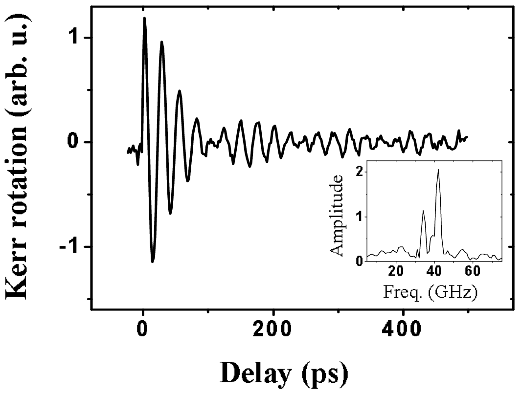
A typical TRKR trace measured with the microscope is shown in Fig. 4. The Kerr rotation angle is plotted in the vertical axis as a function of pump and probe delay. This trace was taken at 4.2 K and 7 Tesla with excitation density photons/cm2 per pump pulse. Pump and probe spots were overlapped and had slightly larger diameters than the optimum values measured before. Oscillations of the Kerr angle in the TRKR trace are due to precession of the optically oriented spins in the applied magnetic field. From the measured precession frequency , the effective g-factor of conduction electrons can be obtained utilizing the relation:
| (2) |
where is Bohr’s magneton, is the applied magnetic field, and is Planck’s constant. Fourier transform of this TRKR measurement (inset in Fig. 4) shows that the signal is composed of two precession frequencies corresponding to two different spin populations in the heterostructure. Using the above equation, g-factor values of and are found. These g-factors correspond to electrons in the 2DEG and electrons in the underlying bulk i-GaAs layers Rizo08 .
The measured Kerr rotation signal decays as a function of time due to several mechanisms. One of these mechanisms is the randomization of the orientation of the transverse component of spins. In analogy with nuclear magnetic resonance, this ensemble dephasing is characterized by the time-constant . Another mechanism that influences the observed signal decay is electron-hole recombination which is characterized by the time constant . Under certain conditions, a net spin polarization remains even after electron-hole recombiation Kikkawa98 , in which case can effectively be regarded as being infinite. If this is not the case, the total decay time-constant of the Kerr signal will be given by: . Additionally, the observed Kerr rotation signal may decay due to diffusion of spin polarized electrons out of the area covered by the focused probe beam. This mechanism is important when the area of the focused probe beam is comparable to or less than , where is the carrier diffusion constant. This mechanism of signal decay must be taken into account when measuring with tightly focused beams as is the case with the microscope described here.
To separate the different contributions to the decay of the total spin signal it is necessary to perform additional experiments. Isolating the spin () and electronic () contributions to requires independently measuring the carrier dynamics. A transient reflectance experiment measures the dynamics of photoexcited carriers irrespective of their spin polarization from which can be determined. Changing from a TRKR configuration to a transient reflectance configuration can be done simply by replacing the photoelastic-modulator with an optical chopper and measuring changes in the total reflected probe intensity induced by excitation with a linearly polarized pump pulse. The carrier diffusion constant can be determined by a transport measurement or utilizing the ability of the microscope to excite (spin polarized) carriers in one location and probe them a certain distance away as will be discussed below.
A remarkable feature of the instrument described here is its ability to measure transport of spin polarized electrons under high magnetic fields. High magnetic fields are crucial, for example, in order to distinguish between different electron populations with slightly different values of . This allows identifying the electron populations that give rise to the signal in spin transport measurements. Such is the case of the heterojunction sample described above. The g-factors of electrons located in the 2DEG and in the bulk layers differ only by a small amount. In order to clearly distinguish between the two electron populations, the difference in their precession frequencies must be comparable to or larger than the Kerr signal decay rate of both spin species. At high enough magnetic fields, the small difference in transforms into a substantial difference in precession frequencies. In this case it becomes possible to identify the contribution to the observed transport of spin polarization from each electron population.
Spin polarization transport was studied in the heterojunction sample in order to determine the nature of the carriers involved in spin transport under high magnetic field and high photoexcitation density. With overlapped pump and probe spots, the Kerr rotation signal amplitude was first maximized by adjusting the focus. Figure 5.a shows the TRKR signal obtained in this configuration at 7 Tesla and 4.2 K. Subsequently, the pump spot was displaced away from the probe spot. In this configuration, the spot profiles and separation were measured by the knife edge technique described earlier (inset in Fig. 5). Spot diameters (FWHM) were measured to be 1.9 m and 3.4 m for the pump and probe respectively. The difference in spot diameters is due to the different central wavelengths of the two beams (780 nm and 820 nm for the pump and probe respectively) and chromatic aberration from the single-element objective lens. The separation between the pump and probe spots is 6 m. From the measured spot diameters the pump photon density is determined to be photons/cm2 while the probe photon density is approximately half of this. This photon density is 3 orders of magnitude higher than the density of electrons in the 2DEG.
The TRKR trace measured with 6 m separation between the pump and probe spots is shown in plot (b) of Fig. 5. With overlapped pump and probe spots (plot (a) in Fig. 5), the amplitude of the Kerr signal decays monotonically with time. This is determined both by the decay of spin polarization and by the diffusion of carriers away from the area covered by the pump and probe beams. The spin polarized carriers that diffuse away from the area covered by the pump are detected when measured with non-overlapped spots. The time it takes for the carriers to diffuse 6 m gives rise to the slow increase in the amplitude of the envelope of the Kerr signal that peaks at a delay of approximately 400 ps. In addition, as will be discussed below, the Kerr signal with separated pump and probe shows coherence up to much longer delays. It is important to note that diffusion takes place predominantly in the plane of the sample and not along the growth direction because the multilayer buffer between the sample substrate and accumulation layer acts as a barrier for carrier diffusion. Fourier analysis of the data taken with non-overlapped spots reveal that only electrons with , that is bulk GaAs electrons, are observed in this measurement.
The signal obtained with non-overlapped spots can be modeled assuming that the width of the Gaussian profile of the carrier density excited by the pump pulse increases with time due to carrier diffusion with diffusion constant . As spin polarized carriers diffuse radially, some enter the region covered by the probe spot increasing the amplitude of the Kerr signal. Spin relaxation also takes place, which ultimately causes a decrease in the Kerr signal amplitude. Analysis of the data reveals that the Kerr signal decay time-constant is 700 ps and the diffusion constant is 70 cm2/s. This value of the diffusion constant is consistent with the conclusion that only bulk GaAs spins contribute to the observed signal since the diffusion constant of 2DEG electrons is more than an order of magnitude larger.
Time-resolved Kerr rotation measured with large diameter (100 m) overlapped spots is insensitive to signal loss due to diffusion of carriers out of the area covered by the laser spots. Experiments with large spots on the same sample and under similar conditions to those discussed above Rizo08 yield a no larger than 300 ps. This is more than two times shorter than the retrieved from the measurements with non-overlapped spots. The reason for the slower spin relaxation rate observed with non-overlapped spots is probably that spin polarized electrons become spatially separated from holes due to their larger diffusion constant. Electron spin-flips due to electron-hole scattering has been shown to be an important spin relaxation mechanism in GaAs quantum-wells Wagner93 ; Gotoh00 .
The Kerr signal decay time constant of 2DEG electrons decreases as the excitation density increasesRizo08 approximately as . This is the reason that at high photon densities only electrons with , i.e., electrons in bulk GaAs, contribute to the Kerr signal. At low photoexcitation densities spin polarized electrons in the 2DEG can be resolved in TRKR measurements as shown in Fig. 4.
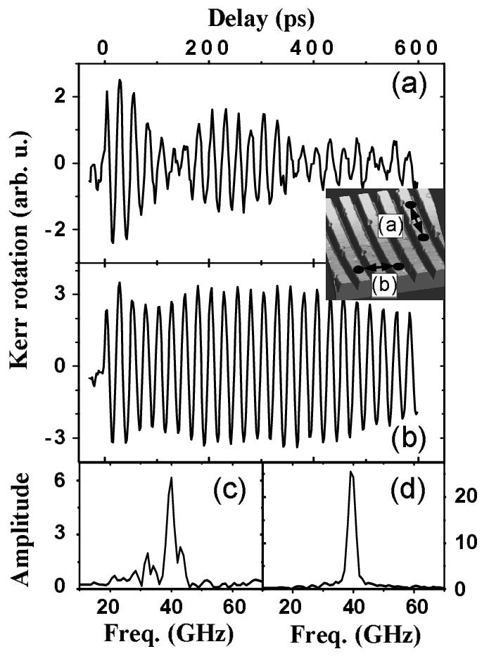
Low excitation density ( photons/cm2) measurements were realized on a single quasi-1D wire fabricated on the heterojunction sample and demonstrate spin transport by 2DEG carriers. A grating structure with 1.6 m period was fabricated on the sample surface by lithography and wet chemical etching. 200 nm wide and 120 nm deep ridges defined channels on the 2DEG of 1.4 m width and 180 m length. Spin transport along one of these channels was measured by TRKR with pump and probe spots separated by 4 m. The result is shown in Fig. 6.a. The Fourier spectrum of this trace shows that two spin populations contribute to the Kerr signal in this configuration: electrons in bulk GaAs and electrons in the 2DEG (peaks at 42 GHz and 32 GHz respectively in Fig. 6.c) Rizo08 . Bulk electrons diffuse isotropically in the plane normal to the growth direction. Quasi-1D electrons, on the other hand, diffuse only along the channel because the ridges of the grating confine the carriers to remain within the channel. For this reason, when the probe spot is focused on a different channel than the pump pulse, no Kerr response from the 2DEG is observed. Figure 6.b shows the TRKR signal measured with pump and probe spots separated by 4 m but each one focused on a different channel. The Fourier spectrum of this measurement, Fig. 6.d, shows no peak at the precession frequency of the 2DEG spins. This experiment demonstrates that the Kerr microscope can measure transport of spin polarization at distances as short as 4 m. The ability to resolve spin transport with such high spatial resolution is essential, for example, for measuring ballistic spin transport where the relevant length scale is of the order of the electron mean free path.
IV Summary
In this article a compact cryogenic sample-scanning microscope designed for static and time-resolved Kerr rotation measurements in high magnetic fields is described. The instrument has spatial resolution of 1 m and temporal resolution utilizing the full laser spectrum of 20 fs. The microscope features the capability of easily changing from Voigt configuration to Faraday configuration due to the use of compact optics and translation systems on the insert of a magneto-optical cryostat with split-coil magnet. The instrument is designed for measuring spin transport in micro and nanostructures and can thus polarize and probe spins at different locations on a device.
The capabilities of the microscope were demonstrated by measuring transport of spin polarization by quasi-1D electrons over micrometer distances such that we can now explore ballistic transport. For these experiments high spatial resolution, high magnetic field operation and the ability to spatially separate pump and probe spots on the sample are necessary.
The power and versatility of the Kerr microscope described above anticipate diverse applications in spintronics such as tracing of spin packet transport in spintronic circuits, investigation of spin-filtering of electric currents in interconnected wire structures Kiselev01 ; Yamamoto05 , mapping the effect of anisotropic spin-orbit fields on spin diffusion in 2D electron systems Meier07 and characterization of ballistic spin transport.
V Acknowledgements
This work is supported by the Zernike Institute for Advanced Materials, by the Dutch Foundation for Fundamental Research on Matter (FOM) and by The Netherlands Organization for Scientific Research (NWO). Two of us (D.R. and A.D.W) acknowledge gratefully financial support of the Deutsche Forschungsgemeinschaft within the SFB491. Special thanks to H. van Driel, U. Douma and A. Kamp from the University of Groningen for the design and fabrication of critical components of the microscope and the controlling and measuring software.
References
- (1) J. M. Kikkawa and D. D. Awschalom Nature 397, 139 (1999).
- (2) G. S. D. Beach, C. Nistor, C. Knutson, M. Tsoi and J. L. Erskine Nat. Mater. 4, 741 (2005).
- (3) C. Nistor, G. S. D. Beach and J. L. Erskine Rev. Sci. Instrum. 77, 103901 (2006).
- (4) M. Atature, J. Dreiser, A. Badolato, and A. Imamoglu Nat. Phys. 3, 101 (2007).
- (5) F.-Y. Lo, A. Melnikov, D. Reuter, Y. Cordier, and A. D. Wieck Appl. Phys. Lett. 92, 112111 (2008).
- (6) C. Meyer, O. Sqalli, H. Lorenz and K. Karrai Rev. Sci. Instrum. 76, 063706 (2005).
- (7) A. Pugžlys, P. J. Rizo, K. Ivanin, A. Slachter, D. Reuter, A. D. Wieck, C. H. van der Wal and P. H. M. van Loosdrecht J. Phys.: Condens. Matter. 19, 295206 (2007).
- (8) P. J. Rizo, A. Pugžlys, A. Slachter, D. Reuter, A. D. Wieck, P. H. M. van Loosdrecht and C. H. van der Wal In preparation.
- (9) J. M. Kikkawa and D. D. Awschalom Phys. Rev. Lett. 80, 4313 (1998).
- (10) J. Wagner, H. Schneider, D. Richards, A. Fischer and K. Ploog Phys. Rev. B 47, 4786 (1993).
- (11) H. Gotoh, H. Ando, T. Sogawa, H. Kamada T. Kagawa and H. Iwamura J. Appl. Phys. 87, 3394 (2000).
- (12) A. A. Kiselev and K. W. Kim Appl. Phys. Lett. 78, 775 (2001).
- (13) M. Yamamoto, T. Ohtsuki and B. Kramer Phys. Rev. B 72, 115321 (2005).
- (14) L. Meier, G. Salis, I. Shorubalko, E. Gini, S. Schön and K. Ensslin Nat. Phys. 3, 650 (2007).