Ill-Contact Effects of d-Orbital Channels in Nanometer-Scale Conductor
Abstract
Electronic current in a nanometer-size rod is theoretically investigated by an eigen-channel decomposition method in nonequilibrium Green’s function formalism. Physical properties, such as the local density of electrons and local current, are decomposed into contributions of eigen-channels. We observe that the evanescent modes and nonlinear conductance are enhanced in d-orbital systems, and the structure of the transmission function, local current density, and penetration depth are discussed. The two effects of the ill-contact at electrodes in d-orbital systems, evanescent modes and the nonlinearity of conductance, are regarded as originating in the peak structure of the transmission function of eigen-channels in the energy region between chemical potentials of left and right lead wires.
1 Introduction
Nonequilibrium current through atomic-scale contact is very important in nanoscience and nanotechnology, where we must know in detail the effects of electrodes. Electrodes themselves can be scatterers for electron transport even if atomic structures are perfectly ordered at electrodes. A decay mode is found in electronic current in nanometer-scale conductance, when the conductor has freedoms of scattering path at each layer. For example, a decay mode is investigated in a monosite chain model with multiple orbitals for each site. [1] The decay mode, evanescent wave, is known also in optics as a nonpropagating mode without dissipation and is of great interest for a possible foundation of nanophotonics. It appears in a nanometer-scale region of material surface, when the light is totally reflected at the surface. [2]
Realistic nanometer-scale conductors, on the other hand, have been studied extensively for their unique structural and transport properties. [3] One can find, for example, quantized conductance in a monatomic wire through a ballistic channel and resonant conductance through a quantized state with strong scattering at electrodes. In nanometer-scale systems, an atomic structure is crucially important for transport properties. [4] The structural investigation is essentially important for discussing quantitative properties of realistic conductance of nanoscale rods. For example, gold appears as a helical multishell nanowire, [5] whose formation was explained with a two-stage process in nanometer-scale phenomena. [6]
We like to discuss, in this paper, the characteristic properties generic in several nanometer-scale rods. Particularly, the possible effect of ill-contact at electrodes in nanometer-scale conductors is investigated, as a combined effect of structural and transport properties. The evanescent wave current appears, when we carry out a channel-decomposition analysis with nonequilibrium Green functions, and the nonlinear conductance under a finite bias voltage is observed.
We will present, in this paper, calculations of an electronic structure, for d-orbital systems of rodlike nanowires of different lengths and widths, which gives prototypical cases for real materials. The generic ill-contact in the electrodes is enhanced in d-orbital systems and becomes an origin of evanescent waves and nonlinear conductance. This paper is organized as follows; In § 2, we review briefly the formalism of the nonequilibrium Green’s function and present the eigen-channel decomposition of Green’s function, local current and other physical quantities. We show several calculated results on the decaying properties of electron density and the nonlinearity of curves in § 3. Section 4 is devoted to the analysis and discussion of the origin of nonlinear conductance and evanescent modes. The penetration of evanescent modes is also discussed. The discussion is focused on two effects of ill-contact in electrodes, the evanescent modes and the nonlinear conductance. The conclusion is given in § 5.
2 Theory of Conductance in Nonequilibrium Green’s Function
We proposed a method of the eigen-channel decomposition of several properties of quantum transport in nanometer-scale conductors by using the nonequilibrium Green’s function (NEGF) formalism. [7, 8] The eigen-channel is the transmission eigenstate obtained by the unitary transformation of the original channels, [9] whose concept may be useful for analyzing current through nanometer-scale metal conductors.
Brandbyge and coworkers obtained the expression for the eigen-channel decomposition of the local density of states (LDOS). [10, 11] We generalize their formulation and provide the decomposition of NEGF and transport quantities, such as the density of electrons or local current, into contributions from respective eigen-channels. This formulation is also applied to the case of finite bias voltage. Information on the eigen-channel decomposition of local current may be necessary for analyzing the vortex of current. [12] Later in the present paper, we will clarify the contribution of ‘evanescent’ modes by eigen-channel analysis.
2.1 Nonequilibrium Green’s function
We use a nanometer-scale metallic rod whose entire system consists of three parts, the conductor (C), the left lead wire (L), and the right lead wire (R). The two lead wires, L and R, are semi-infinite and connect with the central conductor C.
The retarded and advanced Green’s functions and in the conductor C can be obtained within the NEGF theory as [7, 8]
| (1) |
where is the Hamiltonian matrix of the conductor C and its matrix dimension is given as
| (2) | |||||
The coupling of C with the L(R) lead wires is represented by the retarded/advanced self-energies, , which have non-zero elements only near the electrodes.
The lesser Green’s function and the lesser self-energy are defined as [7, 8]
| (3) | |||||
| (4) |
where is a semi-positive-definite matrix given as and is the Fermi-Dirac distribution function in the unperturbed lead wire L (R) of infinite size. The lesser self-energy represents the rate of electron scattering by the electrodes. [13]
We will calculate the self-energies by an efficient recursion method [14] with an appropriate smearing factor and the temperature of electrons in the electrodes is assumed zero. It should be noted that strictly localized states in C without interaction with incoming/outgoing modes in the lead wires are not included in . [15]
2.2 Channel decomposition of physical properties into eigen-channels
The channel-decomposition method was introduced for the local density of states (LDOS) by Brandbyge and coworkers. [10, 11] Now, we are generalizing the method by defining the channel decomposition of NEGF. The theory is formulated with real-space (atomic) bases.
The transmission amplitude matrix from L to R, , and that from R to L, , are given as [16]
| (5) | |||||
| (6) |
An incoming wavefunction of the eigen-channel “” from the left electrode is denoted as the vector , which is an eigen-vector of the matrix . The incoming wavefunction from the right electrode, , is defined in the same manner.
We can define the decomposition of the lesser self-energy into contributions from respective eigen-channels and ;
| (7) | |||||
This definition is a basic idea and, then, the decomposition of the lesser Green’s function can be introduced as
| (8) |
where is defined as
| (9) |
By using this eigen-channel decomposition, the local electron density [7, 8, 14] is decomposed into eigen-channel components;
| (10) | |||||
where is defined as
| (11) | |||||
and is defined in the same manner.
3 Evanescent Wave Modes and Length Dependent Conductance
The presence of the evanescent wave current and nonlinear conductance is demonstrated, in this section, in a nanometer-scale conductor with an electronic structure of s and/or d orbitals, which may be a prototypical model for realistic metals. Here, we adopt the Hamiltonian of spin-unpolarized bulk (fcc) gold (Au) only with s-s or d-d hopping integrals without s-d hybridization in the framework of the tight-binding linear muffin-tin orbital (LMTO) method with the atomic sphere approximation (ASA), [17, 18, 19] specifically the first-order Hamiltonian .
3.1 Gold nanorods: calculated systems
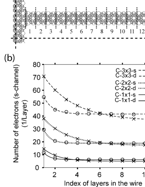
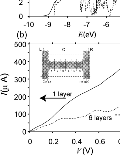
Calculated systems are nanometer-scale conductors: (1) systems of semi-infinite size extending to connecting with a left lead wire, as depicted in Fig. 1(a) and (2) those of finite size connecting with left and right lead wires, as shown in the inset in Fig. 2(b). The conductors and lead wires are quarried from an ideal gold fcc lattice with a lattice constant of a.u. Actual gold nanowires have helical multishell nanostructures [5] whose formation process is explained with the two-stage process based on the quantum molecular dynamical simulation. [6] However, in the present paper, we use the above toy model of gold nanorods with an ideal fcc structure, without lattice relaxation nor reconstruction.
The left lead wire L consists of two layers of 64 atoms and the right lead wire R is the conductor itself of semi-infinite size (Fig. 1(a)) or the left and right lead wires L and R are the same two-layer blocks of 64 atoms of finite size (Fig. 2(b)). The cross sections of the wires C are , , and fcc conventional unit cells. We denote the structures by C-, C-, and C-, respectively. The lengths of the wires are 12 layers for C- and C-, and 9 layers for C-. Each layer consists of two sublayers because of the fcc structure, one atom layer contains five atoms and the other one contains four atoms in each unit ().
The periodic boundary condition is imposed on the plane with the primitive vectors (, , ) and (, , ), and only the point in the - plane is used for the electronic structure calculations. In other words, the cross section of the lead wires is of periodic .
Effects of a bias voltage are added to the Hamiltonian. In the present work, the LDA potential is not determined self-consistently in conductors at a finite bias voltage and a uniform voltage drop of a bias potential is assumed within a conductor. The voltage drop in a conductor may not be uniform in actual nanometer-scale materials but may occur near the regions of contacts where charge distribution would change largely, [11, 20] and the self-consistent calculation for LDA potential in thick nanometer-scale wires may be important for conducting detailed quantitative analysis. The structure of voltage drop presumably depends on the conditions of electrodes and the conductor; for example, in ill-connected electrodes, the voltage drop occurs in the region of electrodes.
3.2 Decaying electron density in rods and evanescent mode
We show the electron density for s- and d-channels in Fig. 1(b) for several semi-infinite size rods (Fig. 1(a)) of different cross sections, in which the local electron density () is integrated with respect to energy and plotted as the sum of each periodic layer;
| (14) |
and we observe the decaying characteristics of electron density. Here, no bias voltage is applied, and electrons enter the system only from the left electrode (, ). The quantity of shows the averaged characteristic among all existing modes. We also calculated the electron density profile in similar periodic systems with a larger cross section of the lead wires of , and no appreciable change was observed. Therefore, we can conclude that the above dependence on the cross section of conductors is universal but not a size effect of the adopted systems. The decaying characteristics of the electron density can be expressed as
| (15) |
and we can define the penetration length .
Figure 1(b) indicates the existence of components of evanescent wavefunction among the modes, which are near-field standing wavefunctions decaying exponentially with increasing distance from the electrode. The components of evanescent wave modes decay owing to backscattering and, therefore, only Bloch wave modes reach the right end (). In other words, when the conductor length is comparable to or smaller than the decay length, the evanescent wavefunctions can reach the opposite electrode. Therefore, one can expect the length dependence on conductance. Note that the comparison between the s- and d-orbital channels is given later in § 4.3.
3.3 Nonlinear conductance with finite bias voltage
The transmission function is defined as [7, 8, 14]
| (16) |
By using eqs. (5) and (6), the transmission function can be decomposed into the eigen-transmission with the unitary matrix in terms of diagonalization of , [21]
| (17) |
The incoming wavefunctions of the eigen-channel from L (the left electrode) can be given by the components of the unitary matrix or .
The current can be evaluated by using the transmission function with the relation [7, 8, 14]
| (18) |
where is the bias voltage applied to the system, is the chemical potential of the L (R) lead wire ().
The length dependence in the conductance of a d-orbital channel is shown in Figs. 2(a) and 2(b) for systems of different rod lengths with a C- cross section. The calculated conductance in Fig. 2(a) shows that the shorter rod has a larger conductance owing to the presence of the evanescent wave modes. In longer systems, the Bloch modes only contribute to conductance. Here, we notice a larger nonlinearity in model systems in the - curve of Fig. 2(b), because a strong resonance scattering in the d-orbital channel causes a strong energy dependence in the transmission function , which will be seen in the next section.
4 Origin of Nonlinear Conductance and Evanescent Modes
4.1 Quantization of one-dimensional modes along rod length in d-orbital channels
Now, we investigate characteristics of the eigen-channels by generalized channel analysis in § 2.
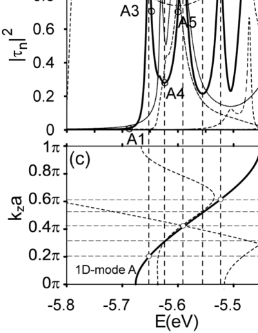
Figure 3(a) shows the eigen-transmissions of the six-layer conductor in Fig. 2, which shows a strong energy dependence or a spiky structure of an energy interval of eV. The eigen-transmission within a narrow energy range () is depicted in Fig. 3(b), in which we focus on the eigen-channel ‘A’. The oscillatory behavior of the transmission function of the eigen-channel A is due to the resonance and off-resonance of one-dimensional Bloch modes.
The d-bands in bulk systems have a width of about 4 eV. Then, the finiteness of the rod radius in the - plane makes each band split. This splitting causes a complicated band-crossing since some d-bands exhibit the dispersion relation , whereas others exhibit the dispersion relation . Then, a complicated branching occurs in d-orbital systems. We plot, in Fig. 3(c), the - curve of the infinite conductor representing the branch of a one-dimensional mode ‘A’ corresponding to the ‘A’-channel.
The right vertical axis refers to the phase of the branch ‘A’ in an infinite periodic wire of fitted effective periodicity length . In fact, the periodic unit length of 4.88 is determined so that the perfect transmission () occurs at the phases of , and 3. This value (4.88) is nearly identical to that of the conductor part (). The fitted length unit of is actually shorter than that of the actual conductor part (), since the wavefunctions are scattered in the regions near the electrode and the resultant effective conductor length should be shortened from that of the ideal one. The above analysis indicates that each eigen-channel (branch) of the d-orbital system has peaks of the transmission corresponding to a phase at . The energy interval between branches is determined by the size of the rod and the structure of d-bands and should be inversely proportional to the radius of the rod. In other words, we have observed two types of nanometer-scale rod quantization; the quantization of the radius of the rod (branch) and that of the length of the rod (peak structure of eigen-transmission).
The oscillatory behavior of resonance and off-resonance in s-orbital channels is relatively weak; [22] one branch extents over a much larger energy range. For example, the energy width of one branch is eV and the energy width of the s-band is about 10 eV in Au. The energy interval of transmission peaks is wider, and the difference between the maximum and minimum values is small. This oscillatory behavior difference may be consistent with the decaying profile of electron density in s- and d-orbital channels in Fig. 1(a), i.e., the evanescent wavefunctions appear in order to connect with wavefunctions in the conductor and lead wires in the electrode region. In the d-orbital channels, more evanescent wavefunctions are necessary than in s-orbital channels, because the wavefunctions have more freedoms of orbital. The strong resonance scatterings causing the large oscillatory behavior in d-orbital channels are consistent with previous works on transition metals. [23, 22, 24]
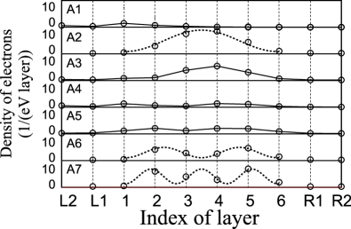
The evanescent wavefunctions of d-orbital channels penetrate much deeper and are more scattered at the electrodes, in order to connect with Bloch modes. This we call the ‘ill-contact’ of d-orbital channels. The channel decomposition of the local density of electrons is shown in Fig. 4 for several energy points A1A7 of the eigen-channel ‘A’ in Fig. 3(b). We can see the characteristics consistent with the above mode analysis results; e.g., the point A1 is placed at the tail position of the branch ‘A’ in Fig. 3 (b) and its local density of electrons exhibits a typical decaying (evanescent) behavior. The point A2 is placed at a peak of the eigen-transmission of the branch ‘A’ in Fig. 3(b) that exhibits a nodeless standing wave, which is consistent with the assignment of the phase of in Fig. 3(c). The density profile shows that the connection of transmission in C and R or L is poor and does not smear out from C.
4.2 Nonlinear conductance and bias voltage dependence of transmission
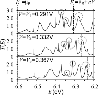
Let us discuss the finite voltage case. The transmission function strongly depends on the bias voltage , as shown in Fig. 5. Furthermore, there exist two characteristic features of d-orbital channels: (i) the negative differential conductance () and (ii) the peak structure in the differential conductance. The differential conductance is separated into two parts:
| (19) | |||||
The first term is the contribution from a new structure of the transmission function entering the energy window () from the higher energy side and is always positive. The second term is the contribution from the change of the overall structure of the transmission function in the energy window and can be negative. Therefore, the negative differential conductance is due to the strong voltage dependence of the overall structure of the transmission function, which is caused by the channels confining the local electron density within the conductor.
The sensitivity of the resonance to the bias voltage is due to the small width of branches of d-bands as a result of ill-contact of d-orbital channels. The peak entering the energy window of from the higher energy side gives rise to the peak of . Therefore, the peak structure of differential conductance originates from that of the transmission due to the resonance scattering.
4.3 Quantization due to finiteness of radius of rod
The mode analysis in § 4.1 indicates that the decaying behavior in Fig. 1(b) appears not only in specific decay modes but also in the sum of various modes, such as those in Fig. 4.
Now, we explain the physical picture of the difference between s- and d-channels for the decaying behavior in Fig. 1. Here, we denote the number of bases of electron wavefunctions on the cross section of the conductor , the energy width of the s- or d-band and that of one branch . For example, one can see from Fig. 3 that eV (the width of the d-bands) and eV (the branch A). should be proportional to the number of atoms on the cross section of the conductor .
A mode can contribute to the current, when it connects with a Bloch wavefunction in the conductor C in the contact region. The number of one-dimensional bands in the conductor C can be estimated as
| (20) |
If the ratio
| (21) |
is small, it is difficult for incoming modes to connect with the one-dimensional Bloch modes in C and majority of the incoming waves may be backscattered. The ratio is, in our examples, of the order of in the d-orbital channels.
The above explanation is consistent with the data in Fig. 1, since the contribution of evanescent modes can be estimated as the difference in local electron density between the left end () and the right end (). In the case of the C--d system, for example, the numbers of electrons at the left and right ends are and , respectively. The contributions of (one-dimensional) Bloch modes () and evanescent modes () are almost the same. The evanescent modes are very important for the d-orbital channels, since .
The same analysis of the s-band system indicates that the evanescent modes are less important () than that in the d-orbital channels, which is consistent with the fact that the ratio is larger than that in the d-orbital channels as because and .
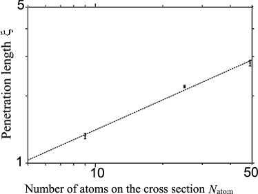
The discussion of the connection is supported by the dependence of penetration length on the number of atoms in the cross section. For simplicity, an extreme case with dispersionless sub-bands is considered for d-orbital channels. In this case, the mean energy interval at Fermi energy is scaled by
| (22) |
Because the penetration length can be estimated as
| (23) |
we obtain
| (24) |
Figure 6 shows the dependence of the penetration length on the number of atoms in the cross section for d-orbital channels for the local electron density in Fig. 1(b) with eq. (15). Because the penetration length is almost scaled by eq. (24), we can conclude that our simple explanation of the connection captures an essential nature of evanescent waves.
It should be noted that a discussion of scattered waves gives the same dependence of the penetration length. Given incident waves are backscattered at edges of the conductor, the collision rate per periodic layer is proportional to , where is the radius of the conductor. Because the penetration length is proportional to the inverse of the collision rate and , eq. (24) is obtained again. This supports our discussion in this subsection.
4.4 Eigen-channel decomposition of local current and evanescent wave modes
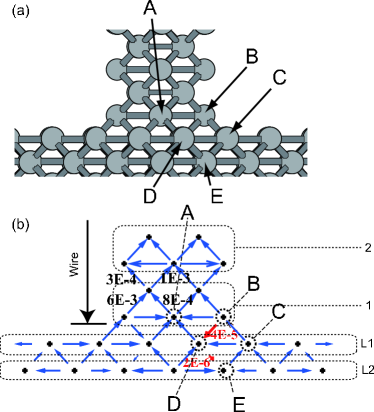
The backward flow cannot be observed even if we would try to observe the total current flow at a certain layer position because of the conservation law of current. In other words, the net flow conserves at each atomic position. Furthermore, no backward flow is observed in the total current flow because of strong forward components of the other modes. Therefore, it is essential to decompose the local current into the eigen-channel components and, then, the eigen-channel current can show the backflow related to the evanescent modes.
We show that the local current defined by eq. (12), using the generalized channel analysis, gives the backward current flow. Figure 7 shows the channel-decomposed local current in eq. (LABEL:def:l-curr) for the channel A1 in Fig. 3. The backward current flow is found, for example, between the atoms and and between the atoms and . The same analysis for the channels A2 and A3 (figure not shown) indicates that the backward current flow appears commonly between the atoms and among the above three channels. The above result supports the discussion in the previous section, in which the evanescent wave component should be attributed not only to decay channels, such as the channel A1, but also to many other channels. Moreover, the observed backward flow should be a net flow of the forward and backward current components and the backward components should be inherent among other regions.
We should emphasize that such backward flow can be obtained, only with the channel decomposition method given in the present paper.
5 Conclusion
An eigen-channel analysis method has been extended to general transport quantities based on the nonequilibrium Green’s function formalism and we studied the transport properties of rodlike nanometer-scale metal wires from the viewpoint of “ill-contact” in d-orbital channels. The ill-contact generates two different characteristics in transport phenomena of d-orbital channels; the evanescent wave modes and nonlinear conductance at a finite bias voltage.
Although the present transport calculation has been carried out only in cases with model structures, the channel decomposition method is general and applicable to realistic materials whose atomic structure is determined by an energy functional with an electronic structure. Such combined simulations of structural and transport properties during the formation of nanoscale structures should be a foundation of nanoelectronics, together with combined experiments of structural and transport observations.
Acknowledgments
Computation was partially carried out using the facilities of the Supercomputer Center, Institute for Solid State Physics, The University of Tokyo. This work was partially supported by a Grant-in-Aid for Scientific Research in Priority Areas “Development of New Quantum Simulators and Quantum Design” (No. 170640004) from the Ministry of Education, Culture, Sports, Science, and Technology, Japan. H.S. thanks JSPS for the financial support.
References
- [1] Y. Asai and H. Fukuyama: Phys. Rev. B 72 (2005) 085431.
- [2] E. Hecht and A. Zajac: Optics (Addison Wesley Publishing Company, 1997, Reading, MA).
- [3] N. Agraït, A. Levy Yeyati, and J. M. van Ruitenbeek: Phys. Rep. 377 (2003) 81.
- [4] J. Bettini, V. Rodrigues, J. C. González, and D. Ugarte: Appl. Phys. A 81 (2005) 1513.
- [5] Y. Kondo and K. Takayanagi: Science 289 (2000) 606.
- [6] Y. Iguchi, T. Hoshi, and T. Fujiwara: Phys. Rev. Lett. 99 (2007) 125507.
- [7] C. Caroli, R. Combescot, P. Nozieres, and D. Saint-James: J. Phys. C 4 (1971) 916.
- [8] Y. Meir and N. S. Wingreen: Phys. Rev. Lett. 68 (1992) 2512.
- [9] M. Büttiker: IBM J. Res. Dev. 32 (1988) 63.
- [10] M. Brandbyge and M. Tsukada: Phys. Rev. B 57 (1998) R15088.
- [11] M. Brandbyge, N. Kobayashi, and M. Tsukada: Phys. Rev. B 60 (1999) 17064.
- [12] S. Nonoyama and A. Oguri: Phys. Rev. B 57 (1998) 8797.
- [13] S. Datta: Electronic Transport in Mesoscopic Systems (Cambridge University Press, 1995, Cambridge) p. 148.
- [14] M. P. López Sancho, J. M. López Sancho, and J. Rubio: J. Phys. F 14 (1984) 1205.
- [15] M. Brandbyge, J.-L. Mozos, P. Ordejon, J. Taylor, and K. Stokbro: Phys. Rev. B 65 (2000) 165401.
- [16] J. C. Cuevas, A. Levy Yeyati, and A. Martín-Rodero: Phys. Rev. Lett. 80 (1997) 1066.
- [17] O. K. Andersen: Phys. Rev. B 12 (1975) 3060.
- [18] O. K. Andersen and O. Jepsen: Phys. Rev. Lett. 53 (1984) 2571.
- [19] O. K. Andersen, O. Jepsen, and D. Glötzel: in Hightlight of Condensed Matter Theory, ed. F. Bassani, F. Fumi, and M. Tosi, (North-Holland, Amsterdam, 1985) p. 59.
- [20] S. Tsukamoto and K. Hirose: Phys. Rev. B 66 (2002) 161402.
- [21] Th. Martin and R. Landauer: Phys. Rev. B 45 (1992) 1742.
- [22] Y. J. Lee, M. Brandbyge, M. J. Puska, J. Taylor, K. Stokbro, and R. M. Nieminen: Phys. Rev. B 69 (2004) 125409.
- [23] E. Tekman and S. Ciraci: Phys. Rev. B 39 (1989) 8772.
- [24] F. Pauly, M. Dreher, J. K. Viljas, M. Häfner, J. C. Cuevas, and P. Nielaba: Phys. Rev. B 74 (2006) 235106.
