Theory of electrical spin-detection at a ferromagnet/semiconductor interface
Abstract
We present a theoretical model that describes electrical spin-detection at a ferromagnet/semiconductor interface. We show that the sensitivity of the spin detector has strong bias dependence which, in the general case, is dramatically different from that of the tunneling current spin polarization. We show that this bias dependence originates from two distinct physical mechanisms: 1) the bias dependence of tunneling current spin polarization, which is of microscopic origin and depends on the specific properties of the interface, and 2) the macroscopic electron spin transport properties in the semiconductor. Numerical results show that the magnitude of the voltage signal can be tuned over a wide range from the second effect which suggests a universal method for enhancing electrical spin-detection sensitivity in ferromagnet/semiconductor tunnel contacts. Using first-principles calculations we examine the particular case of a Fe/GaAs Schottky tunnel barrier and find very good agreement with experiment. We also predict the bias dependence of the voltage signal for a Fe/MgO/GaAs tunnel structure spin detector.
I INTRODUCTION
Semiconductor spintronics aims to harness the electron’s spin degree of freedom in data storage and processing, typically by utilizing heterostructures composed of a combination of magnetic and non-magnetic materials Zutic et al. (2004). A fundamental problem in semiconductor spintronics was to find ways to electrically generate non-equilibrium electron spin distributions in conventional semiconductors. Efficient electrical spin injection from ferromagnetic contacts into semiconductors using spin dependent tunneling Rashba (2000), Smith and Silver (2001) was shown to overcome the ’conductivity mismatch problem’ associated with highly conductive metallic contacts Schmidt et al. (2000). Spin polarization of the tunneling current originates from the spin dependence of the electron wavefunctions and the densities of states of the ferromagnetic contact. The spin dependent tunneling approach was realized experimentally using Fe interfaces with GaAs Hanbicki et al. (2002, 2003); Adelmann et al. (2005); Crooker et al. (2005); Lou et al. (2007a), silicon Huang et al. (2007); van ’t Erve et al. (2007) and graphene Tombros et al. (2007). Jiang et. al using CoFe/MgO interfaces showed enhanced electrical spin injection efficiency into GaAsJiang et al. (2005). Contacts made of CoFe were also used to inject directly into GaAs Kotissek et al. (2007) and showed an electron polarization that had dramatically different bias dependence from that of Fe/GaAs contacts Lou et al. (2007a). In addition to electrical spin injection, efficient electrical spin detection is required to achieve functional semiconductor spintronic devices.
Crooker et al exp recently reported experiments of electrical spin detection using Fe/GaAs Schottky tunnel barriers as electrical spin detectors. They demonstrated that both the magnitude and sign of the spin detection sensitivity are tunable with voltage bias applied across the Fe/GaAs interface; in some cases they were able to improve the spin detection sensitivity by an order of magnitude. The bias dependence of the sensitivity of the detector was shown to be dramatically different from that of the injected current spin polarization. A theoretical model was used to correlate the spin-detection sensitivity of the Fe/GaAs electrodes with their bias-dependent spin injection properties. The model described successfully many of the experimentally observed trends exp .
Here we give a detailed description of this theoretical model of electrical spin detection at a ferromagnet/semiconductor interface. We consider a case when spin polarization is generated in the semiconductor by an external source (e.g., optical or electrical) and subsequently detected at a ferromagnetic contact in which a tunnel barrier exists at the ferromagnet/semiconductor interface. We incorporate first principles calculations to examine two specific cases of tunnel barrier, a Fe/GaAs Schottky tunnel barrier and a Fe/MgO/GaAs tunnel structure. In this way we demonstrate that the theory is general and can be applied to a variety of electrical spin detectors. We show that the sensitivity of the electrical spin detectors have strong bias dependence of both microscopic and macroscopic origin. While the bias dependence of microscopic origin is specific to each ferromagnet/semiconductor tunneling structure, the macroscopic bias dependence is general and depends on the electrical transport properties of the semiconductor.
This article is organized as follows. In Section II we give a detailed description of the theory. At the end of the section we provide some approximate analytical formulas and look at the asymptotic limit of large currents. This helps in understanding the general trends predicted by the theory and facilitates a discussion of the numerical results. In section III, first we present numerical results for a generic spin detector with a tunneling current polarization that has no bias dependence, then we incorporate first principles calculations to examine the specific cases of Fe/GaAs Schottky barrier and Fe/MgO/GaAs tunnel structure spin detectors. We conclude the paper in Section IV. with a summary of our results and conclusions. Some calculational details are included in an appendix.
II THEORETICAL MODEL
A voltage signal, in response to a change in the spin polarization of the current, at a ferromagnetic tunnel junction results because the tunneling resistance of the junction depends on electron spin. For example, if the tunneling resistance of junction is smaller for spin-up (majority spin in the ferromagnetic contact) electrons than for spin-down electrons (minority spin in the ferromagnetic contact), the voltage drop across the junction will decrease if the spin-up electron component of the current increases while the spin down electron component of the current decreases keeping the total current constant. In recent experiments reported by Crooker et al exp , the spin polarization of the current at the tunnel junction is changed either by the absorption of circularly polarized light in the semiconductor in the vicinity of the ferromagnetic tunnel junction or by electrical injection from a remote ferromagnetic contact. The spin polarized electron density generated by the absorption of the circularly polarized light or remote electrical injection drift/diffuses to the detection ferromagnetic tunnel junction and thus modifies the spin polarization of the current across this junction. A bias dependence of the voltage signal, as is observed experimentally, occurs because of a combination of two effects: 1) transport of the remotely generated spin polarized electron density depend on bias so that the change in spin polarization of the current crossing the tunnel junction depends on voltage bias; and 2) the spin dependence of the tunneling resistance depends on voltage bias.
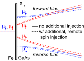
Fig. 1 shows a schematic diagram of the electro-chemical potentials for spin-up and spin-down electrons in the vicinity of a ferromagnetic tunnel junction in which the junction resistance is smaller for spin-up electrons than for spin-down electrons. We show for the cases under reverse bias (electron injection into the GaAs) and under forward bias (electron extraction from the GaAs), without remote spin generation (solid lines) and with remote generation of spin-up electrons (dashed lines). The Fe contact is highly conductive so that the electric field in the Fe is very small and the spin-up and spin-down electron distributions in the Fe are very nearly in equilibrium with each other. Thus, in the Fe, the electro-chemical potentials for the two spin types are nearly constant in position and equal to each other independent of bias. The shaded stripe in Fig.1 represents the depletion region in the GaAs that forms the tunnel barrier. There is a drop in the electro-chemical potential across this tunnel barrier region for both spin-up and spin-down electrons. This drop in electro-chemical potential is proportional to the product of the current and the tunnel resistance for each spin type. It is larger for spin-down electrons than for spin-up electrons because the tunneling resistance is larger for spin-down electrons than for spin-up electrons. In reverse bias, the electro-chemical potentials are higher in the Fe contact than in the GaAs and because the drop across the junction is larger for spin-down electrons than for spin-up electrons there is a surplus of spin-up electrons compared to spin down electrons near the junction interface. In forward bias the electro-chemical potentials are higher in the GaAs than is the Fe contact and there is a surplus of spin-down electrons compared to spin-up electrons near the junction interface. Because of spin relaxation, the electro-chemical potentials for spin-up and spin-down electrons come together far from the tunnel junction when there is no spin generation. When there is generation of spin-up electrons, the two electro-chemical potentials far from the tunnel junction remain separated and are determined by the spin generation profile. At any point in space the spin polarization of the density is determined by statistics from the electro-chemical potentials and the spin polarization of the current is determined by the product of the density and the spatial derivative of the electro-chemical potential for each spin type. The voltage signal at the tunnel junction produced by optical spin generation depends on the change in spin polarization of the current at the tunnel junction and the tunneling resistance of each spin type.
To describe theoretically the voltage signal we use the 1-dimensional model of Ref. Smith and Silver, 2001 with some modifications. In this model the current flow at the interface is described using a spin dependent interface conductance:
| (1) |
where is the current density at the interface, is the interface conductance, the interfacial discontinuity in electrochemical potential for electrons with spin projection , and is the magnitude of the electron charge. We set the interface at the position with the ferromagnet on the left side () and the semiconductor on the right (). As in Ref. Smith and Silver, 2001, we define a variable such that , where is the total current density (independent of position in the 1-dimensional model) and a variable such that , where is the electron density in the semiconductor which is independent of position and of bias. Eq. (1) can be written as:
| (2) |
and
| (3) |
where is the electro-chemical potential for electrons at the right (left) side of the interface and is evaluated at the interface. Adding equations (2) and (3) gives
| (4) |
and subtracting them yields
| (5) |
The voltage drop at the interface is
| (6) |
so that
| (7) |
We consider a case in which the electrons in the semiconductor are strongly degenerate and relate the electrochemical potentials and the densities using a zero temperature Fermi function, then
| (8) |
and
| (9) |
where is the Fermi energy and is evaluated at the interface.
We describe the current flow in the semiconductor using spin dependent drift-diffusion equations
| (10) |
where is the diffusion coefficient, is the electric field in the semiconductor (independent of position in the 1-dimensional model), and is the electron mobility. The drift-diffusion equation at the interface gives:
| (11) |
If electrons with different spins are driven out of local quasi-thermal equilibrium at some region in space, so that is not equal to , the difference in the two electron densities relax as described by the spin current continuity equation
| (12) |
where is the spin-relaxation time and is the spin generation function.
We are interested in how the interface voltage drop varies with small changes in the amplitude of the spin generation function where is a unitless and normalized function of position. The voltage signal depends on the amplitude of the spin generation function through the spin polarization of the current at the interface Ref. G, V(
| (13) |
The voltage signal depends on the derivative of and with respect to C and to calculate these derivatives we use Eq. (12). We search for a solution of this equation of the form subject to boundary conditions and where is the solution of the homogeneous differential equation and is the Green’s function solution of
| (14) |
with boundary conditions and . For a general spin generation function, we have
| (15) |
where
| (16) |
and
| (17) |
Using , where is the conductivity of the semiconductor, and the Fermi liquid relationship , we can write as
| (18) |
To be specific, we consider a striped spin generation function of the form:
| (19) |
where is the center position of striped spin generation and is its width (). Then Eq. (11) can be written as
| (20) |
where in general
| (21) |
For the striped spin generation function and depends on current through . (F(j) is negative because is negative). Because , and this can be written in terms of the values of parameters and at the interface.
| (22) | |||||
Considering that on the metal side of the interface the electrochemical potentials for spin and electrons are very nearly equal, Eqs. (5), (8) and (9) give
| (23) |
Equations (22) and (23) together give and for any given value of the amplitude of the source function and of bias. Eq. (23) is non-linear and is solved numerically for after elimination of with the help of Eq. (22). The spin-detection sensitivity, defined as , and the current polarization, , are then calculated numerically.
Before we present the numerical results of the model, it is instructive to linearize Eq. (23), in order to obtain an analytic expression for valid for weak injection conditions. For the linear case it is convenient to rewrite Eqs. (22) and (23) in terms of a parameter because is close to :
| (24) |
| (25) |
where . We eliminate from the second equation and differentiate with respect to
| (26) |
| (27) |
where
| (28) |
When the density polarization is small and . In this case, we can linearize
| (29) |
The current polarization is given by,
| (30) |
We note in passing that equations (30) and (7) combined can be used to extract and from the exerimental data set of total current, voltage and current polarization.
Equations (29), (27) and (26) give an analytic expression for , which in terms of the parameter can be written as
| (31) |
In the derivation of Eq. (26) we kept the diffusion (first RHS term) and drift (second RHS term) contributions to the voltage change separate. The diffusion term has two contributions. The term is always positive. It describes the change of current polarization at the interface, due to diffusion, resulting from the Green’s function term in Eq. (15). The term is always negative because is positive. It describes the change of current polarization at the interface, due to diffusion, resulting from the homogeneous solution term in Eq. (15) The drift term, , describes the change in spin current polarization at the contact from drift of the modified spin density polarization at the interface due to external spin generation. Its sign depends on the sign of . For spin injection () the absolute value of cannot be larger than and hence the diffusion term is always positive. The drift term is always negative and therefore the two processes always oppose each other for spin injection. For spin collection () is smaller than for small currents but can become larger than for large currents. As a result the diffusion term is positive for small currents, but can become negative for large currents and the drift and diffusion augment each other for small currents but can oppose each other for large currents in spin collection.
It is interesting to examine the asymptotic behavior for large bias lar of . When , we can write
| (32) |
For the case of spin collection, where j is positive, this becomes as
| (33) |
Then we have
| (34) |
where and
| (35) |
so that
| (36) |
Part of the diffusion term (RHS first term) cancels exactly the drift term (RHS second term) leaving a linear dependence on ,
| (37) |
Note that F(j) is always negative and for the case of a homogeneous source .
For the case of spin injection, where j is negative, Eq. (32) can be written as
| (38) |
Then,
| (39) |
and
| (40) |
so that
| (41) |
The first two RHS terms are the diffusion and the third the drift contributions to the change of current spin polarization at the interface due to external spin generation. The leading order terms in have opposite signs and cancel. Then to leading order in ,
| (42) |
and
| (43) |
Unlike spin collection where the spin detection sensitivity grows linearly with , during spin injection spin sensitivity drops as . It is worth mentioning that the exact cancellation of leading order terms in Eq. (41) occurs strictly in the 1D case, but there is no physical principle that demands exact cancellation for a more complicated geometry. This may lead to a reversal of the sign of the voltage signal with bias for spin injection.
III RESULTS
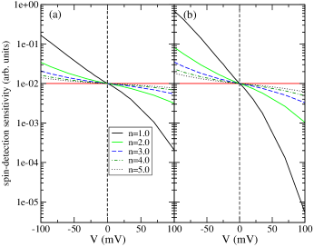
We present results of the model from numerically solving the nonlinear equations. In the following, in order to facilitate the comparison with experiments we adopt the convension that negative voltage corresponds to spin collection and positive voltage to spin injection. Often, as is done in experimental works we will refer to the negative voltage as forward bias and to the positive voltage as reverse bias. In Fig. 2 we show the calculated spin detection sensitivity for an electrical spin detector with an interface which has a constant current spin polarization (independent of bias). Required inputs to the calculation of the voltage signal are: electron density, mobility, spin lifetime, and the spin tunneling conductances . The left panel in Fig. 2 is for mobility 3000 and the right for 1500 . We have used several values for carrier concentrations and they are shown in the plot. The spin-relaxation time is set to . The source is set at a distance of from the Fe/GaAs interface and it has a width of , the source function is constant within this interval. As seen in Fig 2, in all cases, for spin injection the magnitude of the calculated voltage signals drops rapidly with increasing bias even though the current polarization is constant. By contrast, the magnitude of the calculated voltage signals, increases rapidly with increasing bias during spin collection. The difference between the calculated voltage signal and current polarization is larger for smaller values of the electron mobility and electron concentration. The magnitude of the voltage signal is smaller than the current polarization in reverse bias but larger in forward bias for a combination of two reasons: 1) the drift and diffusion contributions to Eq. (26) oppose each other in spin injection but add in spin collection; and 2) the electric field in the semiconductor tends to drift the optically or electrically generated spin polarized electrons away from the detector contact in reverse bias but toward the detector contact in forward bias. When the semiconductor is more heavily doped the electric field is smaller therefore these effects are less pronounced than when the semiconductor is more lightly doped. More specifically, from equations (43) and (37) we can see that the rate of drop/increase depends on the conducting properties of the semiconductor, the spin polarization of the interface (prefactor ) and the location and width of the spin source (prefactor ). The rate of increase during spin collection is proportional to while the rate of decrease is proportional to
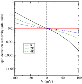
In Fig. 3 we show the influence of the tunneling resistance. In a ferromagnet/semiconductor interface the tunneling resistance depends on the Schottky barrier height, width and shape. The first is determined by the magnitude of the band gap in the semiconductor and the position of the Fermi level relative to the top of the valence band while the last two are modulated with doping. In Fig. 3 we can see that smaller tunneling resistance results in bigger variation of spin detection sensitivity with bias. This can be understood by from the linearized results in Eq. (43).
The rate of change of spin detection sensitivity with bias is inversely proportional to the tunneling resistance. The physical origin of this lies in that, for a given applied voltage, larger tunneling resistance will result in smaller current; this is reducing the effect of drift.
Generally speaking, the current spin polarization and hence can have a strong bias dependence. It was shown in Ref. Crooker et al., 2005; Lou et al., 2007b; Chantis et al., 2007a that the current spin polarization of Fe/GaAs(001) junctions has a very strong bias dependence, and even reverses sign within a small interval around zero bias. In Ref. Chantis et al., 2007a; Dery and Sham, 2007 two different microscopic models to explain the experimentally observed bias dependence of the tunneling current were discussed. The bias dependence of spin sensitivity is due to a combination of the macroscopic physics described above and the microscopic bias dependence of . To predict the resulting behavior in specific ferromagnet/semiconductor junctions we have incorporated our model first-principle results for the bias dependence of .
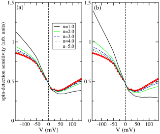
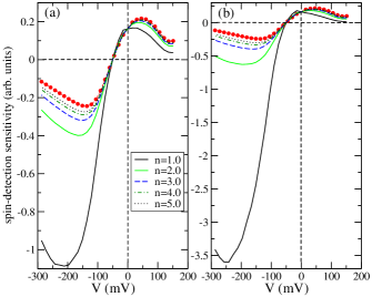
In Fig. 4 we show the calculated spin detection sensitivity and first-principles current polarization for a Fe/GaAs(001) interface. The first-principle method and results are identical to that presented in Ref. Chantis et al., 2007a. As it was explained in Ref. Chantis et al., 2007a the interface electronic structure of Fe/GaAs(001) results in two strong minority-spin peaks in the energy dependence of electron transmission across the interface. One is located at about 125 meV below and the other 125 meV above. The result is a strong bias dependence of the current spin polarization. We see in Fig. 3 that the bias dependence of spin detection sensitivity bares some resemblance to that of the current spin polarization but in the general case can be significantly different. The magnitude of decreases (increases) faster than the spin polarization in the negative (positive) bias and the difference between the two increases as we make the semiconductor less conductive. As we can see in Fig. 4 the spin detection sensitivity can be raised by an order of magnitude in the positive bias. Therefore, under certain conditions the macroscopic factors described above can have a dominant influence over the microscopic factors that influence the bias dependence of current polarization. Since it is much easier to control the conducting properties of semiconductor rather the microscopic electronic properties of the interface, these effect can have a direct application in optimization of electrical spin detectors. This result is in very good agreement with the experimental bias dependence of spin-detection sensitivity presented in Ref. exp, .
It is interesting to examine the bias dependence of spin-detection sensitivity for a different interface. The Fe/MgO(001) interface is different from Fe/GaAs(001) in many ways and it is of great interest to spintronics community. To calculate the spin-dependent tunneling conductance of Fe/MgO(001) we used the same approach as in Ref. Chantis et al., 2007a, b; Chantis et al., 2008 and the same setup with Ref. Belashchenko et al., 2005. The details of the calculation such as the chosen k-mesh in the two dimensional Brillouin zone (2DBZ) and the method of calculation for the total current and spin polarization are the same with those used for Fe/GaAs(001) interface and are described in Refs. Chantis et al., 2007a, b. It was shown in Ref. Belashchenko et al., 2005; Khan et al., 2008 that the interface minority-spin resonances in Fe/MgO(001) interface are located far from the point in the 2DBZ, contributing much less to the tunneling conductance than they do in the case of Fe/GaAs(001) interface. Therefore as we can see in Fig. 5 the spin polarization of the tunneling current has less dramatic bias dependence in this case. The band gap of MgO is about 5 times larger than the band gap of GaAs so the Fe/MgO tunneling barrier has much bigger resistance than the Fe/GaAs. Because of these differences with Fe/GaAs interface the spin-detection sensitivity is much less sensitive to the changes in applied bias. This is consistent with the analysis given so far and in particular with Eq. (43).
IV CONCLUSION
We presented a theory of electrical spin detection in ferromagnet/semiconductor detectors. We showed that the sensitivity of such detectors can have a strong bias dependence. The origin of this dependence lies in the microscopic electronic structure of the interface and the macroscopic electrical properties of the conducting channel in the semiconductor. The first was incorporated in our model with the help of first principles electronic structure calculations. With the help of a model spin detector which has constant current polarization with respect to bias we showed that the latter by itself is capable of producing strong bias dependence of sensitivity. This result suggests that enhancement of detector’s sensitivity is possible independent of the materials used to construct the detector by engineering the electrical properties of the conducting channel in the semiconductor and tuning the bias. Our results for the particular case of Fe/GaAs Schottky tunnel contacts show a very good agreement with experiment exp . As in the experiment we were able to enhance the spin sensitivity by an order of magnitude when applied positive voltage. Our results for Fe/MgO/GaAs show a similar enhancement though the magnitude of the effect is smaller than in Fe/GaAs. This is explained by the bigger height of tunneling barrier in the case of Fe/GaAs. These results suggest specified routes on how to engineer efficient electrical spin detectors using ferromagnet/semiconductor interfaces.
Acknowledgements.
This work was supported by DOE Office of Basic Energy Sciences Work Proposal Number 08SCPE973. We thank S. A. Crooker and P. A. Crowell for many valuable discussions.V Appendix: Voltage Derivative of the Interface Conductances
In the previous sections we neglected terms proportional to the voltage derivative of the interface conductances because these terms are small for typical parameter values. In this appendix we discuss the contribution of these terms. For notational simplicity, it is convenient to define
| (44) |
and
| (45) |
In this notation the voltage drop at the interface is
| (46) |
where P is the current density spin polarization . Including the voltage derivative of the interface conductances gives the voltage signal as
| (47) |
where is the new term. Solving for gives
| (49) |
where
| (50) |
References
- Zutic et al. (2004) I. Zutic, J. Fabian, and S. D. Sarma, Reviews of Modern Physics 76, 323 (pages 88) (2004), URL http://link.aps.org/abstract/RMP/v76/p323.
- Rashba (2000) E. I. Rashba, Phys. Rev. B 62, R16267 (2000).
- Smith and Silver (2001) D. L. Smith and R. N. Silver, Phys. Rev. B 64, 045323 (2001).
- Schmidt et al. (2000) G. Schmidt, D. Ferrand, L. W. Molenkamp, A. T. Filip, and B. J. van Wees, Phys. Rev. B 62, R4790 (2000).
- Hanbicki et al. (2002) A. T. Hanbicki, B. T. Jonker, G. Itskos, G. Kioseoglou, and A. Petrou, Appl. Phys. Lett. 80, 1240 (2002).
- Hanbicki et al. (2003) A. T. Hanbicki, O. M. J. van ’t Erve, R. Magno, G. Kioseoglou, C. H. Li, B. T. Jonker, G. Itskos, R. Mallory, M. Yasar, and A. Petrou, Appl. Phys. Lett. 82, 4092 (2003).
- Adelmann et al. (2005) C. Adelmann, X. Lou, J. Strand, C. J. Palmstrom, and P. A. Crowell, Phys. Rev. B 71, 121301 (2005).
- Crooker et al. (2005) S. A. Crooker, M. Furis, X. Lou, C. Adelman, D. L. Smith, C. J. Palmstrom, and P. A. Crowell, Science 309, 5744 (2005).
- Lou et al. (2007a) X. Lou, C. Adelman, S. A. Crooker, E. S. Garlid, J. Zhang, K. S. M. Reddy, S. D. Flexner, C. J. Palmstrom, and P. A. Crowell, Nature Physics 3, 197 (2007a).
- Huang et al. (2007) B. Huang, D. J. Monsma, and I. Applebaum, Phys. Rev. Lett. 99, 177209 (2007).
- van ’t Erve et al. (2007) O. M. J. van ’t Erve, A. T. Hanbicki, M. Holub, C. H. Li, C. Awo-Affouda, P. E. Thompson, and B. T. Jonkervan, Appl. Phys. Lett. 91, 212109 (2007).
- Tombros et al. (2007) N. Tombros, C. Jozsa, M. Popinciuc, H. T. Jonkman, and B. J. van Wees, Nature 448, 571 (2007).
- Jiang et al. (2005) X. Jiang, R. Wang, R. M. Shelby, R. M. Macfarlane, S. R. Bank, J. S. Harris, and S. S. P. Parkin, Phys. Rev. Lett. 94, 056601 (2005).
- Kotissek et al. (2007) P. Kotissek, M. Bailleul, M. Sperl, A. Spitzer, D. Schuh, W. Wegscheider1, C. H. Back1, and G. Bayreuther, Nat. Phys. 3, 872 (2007).
- (15) S. A. Crooker, et al, arXiv:0809.1120.
- G (V() Experimentally the change in voltage, at constant current, is measured as the spin generation, , is varied. Because the interface conductances are voltage dependent and the voltage changes with changes in , there are also terms proportional to the voltage derivative of the interface conductances. These terms are small for typical parameter values. These terms are easily included, but we neglect them here for algebraic simplicity and include a discussion of them in the appendix.
- (17) The linearity condition can be violated at large bias if the the interface conductances are strongly spin dependent. The asymptotic results described here are qualitative. The numerical results, presented in the next section, do not assume the linearity condition.
- Lou et al. (2007b) X. Lou, C. Adelman, S. A. Crooker, E. S. Garlid, J. Zhang, K. S. M. Reddy, S. D. Flexner, C. J. Palmstrom, and P. A. Crowell, Nature Physics 3, 197 (2007b).
- Chantis et al. (2007a) A. N. Chantis, K. D. Belashchenko, D. L. Smith, E. Y. Tsymbal, M. van Schilfgaarde, and R. C. Albers, Phys. Rev. Lett. 99, 196603 (2007a).
- Dery and Sham (2007) H. Dery and L. J. Sham, Phys. Rev. Lett. 98, 046602 (2007).
- Chantis et al. (2007b) A. N. Chantis, K. D. Belashchenko, E. Y. Tsymbal, and M. van Schilfgaarde, Phys. Rev. Lett. 98, 046601 (2007b).
- Chantis et al. (2008) A. N. Chantis, T. Sandu, and J. Xu, PMC Physics B 1:13 (2008).
- Belashchenko et al. (2005) K. D. Belashchenko, J. Velev, and E. Y. Tsymbal, Phys. Rev. B 72, 140404 (2005).
- Khan et al. (2008) M. N. Khan, J. Henk, and P. Bruno, J. Phys.: Condens. Matter 20, 155208 (2008).