Band bending and quasi-2DEG in the metallized -SiC(001) surface
Abstract
We study the mechanism leading to the metallization of the -SiC(001) Si-rich surface induced by hydrogen adsorption. We analyze the effects of band bending and demonstrate the existence of a quasi-2D electron gas, which originates from the donation of electrons from adsorbed hydrogen to bulk conduction states. We also provide a simple model that captures the main features of the results of first-principles calculations, and uncovers the basic physics of the process.
pacs:
73.20.-r, 73.21.Fg, 71.15.MbThe Si-rich -SiC(001) surface has been reported to become metallic when exposed to atomic hydrogen amy ; natmat . This is quite surprising, as H-saturation of semiconductor surfaces normally leads to passivation. The experimental work has shown that the metallization does not involve the surface silicon dimers, which are passivated upon hydrogen or water exposure amy . It was early speculated that the metallization was caused by the incorporation of hydrogen in deeper layers, and more specifically in the troughs of the reconstruction. Recent theoretical works difelice ; chang ; peng have shown that this is a plausible (although not thoroughly accepted) explanation for the surface metallization. Fig. 1 shows the band structure of the proposed configuration (schematically shown in the inset), obtained from a Density Functional Theory (DFT) calculation method in a thick slab containing the top Si layers plus 12 C-Si bilayers. The shadowed area shows the projection of the bulk band structure, which is positioned with respect to the surface bands by aligning the electrostatic potential of the bulk with that of the slab calculation at a depth where this potential becomes flat. The surface is clearly metallic, with several band crossing the Fermi level.
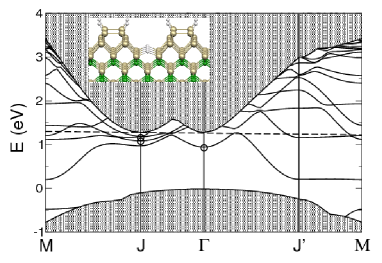
As discussed by other authors difelice ; chang ; peng , while some of the metallic bands correspond to surface states, others come from states deriving from the conduction band of the host SiC crystal. These states can be seen in Fig. 1 as parabolic bands split off the conduction band minima at the and points of the Surface Brilloiun Zone (SBZ), while the extended conduction band states remain above the Fermi level. In this letter, we study these interesting and quite unexplored aspects of this surface, and show how these states become localized near the surface forming quantized quasi-two dimensional states due to band bending effects.
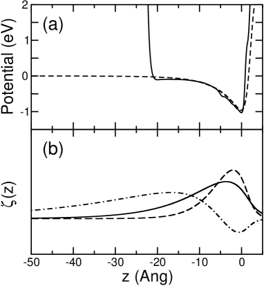
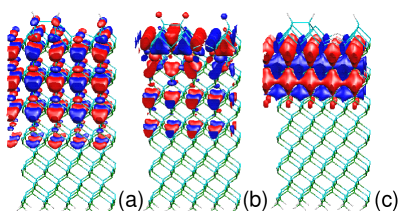
The key to understand surface metallization is the realization that incorporation of hydrogen to the in-trough sites leads to transfer of electrons from the Si-H-Si center to surface and conduction bands that were unoccupied prior to hydrogen incorporation. The separation of charges leads to electric fields which produce a strong band bending near the surface. Fig. 2(a) (full line) shows the averaged electrostatic potential macroave obtained in our DFT slab calculations as a function of the depth. These results show the presence of electric fields at depths of more than 10 Å from the Si-rich region, well into the host SiC material. This band bending acts as a quantum well potential that produces quantization of the conduction band states, which become localized in the direction perpendicular to the surface. Fig. 3 shows these states, as obtained in the DFT calculations.
To provide a deeper understanding of the band bending and the appearance of quantized states, we present a simple model which captures the physics of the system. We use the method proposed by Stern and Howardstern ; ando to study semiconductor inversion layers. We only consider the electrons donated to the conduction band by the in-trough adsorbed hydrogen atoms. The rest of the electrons (including those donated to surface bands) are not considered explicitly, since they do not contribute significantly to band bending effects. We work within the effective mass approximation, using the effective mass tensor corresponding to the bottom of the conduction band. Since we are dealing with the (001) surface orientation, the conduction band has three minima in the SBZ of the 11 surface reconstruction. The minima correspond to the conduction band valleys at the points of the bulk -SiC Brillouin zone, giving three ellipses with longitudinal and transverse masses of 0.68 and 0.25 , respectivelykaplan . Two of the ellipses have their longitudinal mass in the surface plane, and are centered at the points of the -SiC(001) 11 SBZ. The third one has its longitudinal mass along the direction perpendicular to the surface, and is centered at the point of the -SiC(001) 11 SBZ. Note that the and points of the 11 reconstruction fold down to the and points of the 32 reconstruction, which is the reason why the minima of the SiC bulk conduction bands projected in the 32 SBZ appear, at the same energy, at and in Fig. 1
By the use of the effective mass approximation, the problem is reduced to finding the solutions of the potential in the direction perpendicular to the surface, while in the parallel directions the solutions are plane waves with parabolic dispersion. We model the effective potential seen by the electrons as the contribution of two terms. The first one represents the confining potential at the surface, which keeps the electrons inside the bulk. Consistently with the effective mass approximation, this potential is taken as zero inside the bulk and to raise smoothly at the surface to reach the vacuum level outside the solid. Here, is the energy required for an electron at the bottom of the conduction band to escape the surface, which we estimate from the difference between the work function of the clean surface and the energy gap of SiC, resulting in a value of 3.5 eV. The second term describes the electrostatic attraction between the conduction electrons and the net compensating positive charge at the surface layers, as well as the repulsion between the conduction electrons. The latter is described in the Hartree approximationstern , thus neglecting exchange and correlation effects. The electrostatic term is related to the charge density of the conduction band electrons and the associated positive charge left in the adsorbed hydrogen atoms by Poisson’s equation.
We solve numerically the 1D Schrödinger effective mass equations relating the potential and the wavefunctions and their energies for each of the conduction band valleys of the SiC(001) surface. Here, or indicates the longitudinal or transversal valley, and is an index labeling each of the bound solutions. The bound states are occupied up to the Fermi level, which is determined by the number of electrons donated by the adsorbed hydrogen atoms. In all the calculations, the electronic temperature was set to zero, so the electronic occupations follow the step function distribution (i.e., there are no thermally excited carriers). Once the occupations of the bound states are determined, the charge density is constructed and Poisson’s equation is solved numerically to obtain the updated effective potential . This procedure is repeated until self-consistency is achieved.
The self-consistent electron potential obtained from the model is shown in Fig. 2(a). It is very similar to the DFT potential, which clearly shows that the origin of the band bending is the donation of electrons to the conduction band. For the quantized wave functions, we obtain three bound solutions. For the ellipse perpendicular to the surface, we obtain two bound states, at energies 0.34 and 0.01 eV below the bottom of the bulk conduction band, shown in dashed and dot-dashed lines in Fig. 2(b), respectively. This ellipse corresponds to states at the point of the 32 SBZ. In the DFT results shown in Fig. 1, only one bound state is observed, with an energy close to that found in the model for the lowest state. The higher one is not seen as a bound state in the DFT calculation, a discrepancy which is explained by the finite thickness of the slab used in the DFT calculation (note that this state extends several tens of Ångström from the surface, much more than the slab thickness). For the ellipses parallel to the surface plane, we obtain only one bound state (full line in Fig. 2(b)), with an energy 0.16 eV below the bulk conduction band, which is doubly degenerate due to the existence of two equivalent ellipses. It corresponds to states in the point of the 32 SBZ. In the DFT calculation, due to the presence of the surface reconstruction that breaks the crystal symmetry in the plane (due to the presence of the dimer rows and troughs), these two states mix up and split. Also, they mix with other surface states at similar energies at the point point. The resulting DFT wave functions are those shown in Fig. 3(a)-(b). We note that the lower binding energy and larger spatial width of this state compared to the most bound state of the ellipse perpendicular to the surface is due to the smaller effective mass of the electrons in the direction.
Both in DFT and in the simple model, the underlying bulk SiC crystal is assumed to be an intrinsic semiconductor at T=0oK. Therefore, there are no free carriers available from the bulk. The band bending effects described here are not due to screening of surface dipoles or charges by bulk carriers, as it is the usual case in semiconductor surfaces and interfaces. It is purely due to the carriers donated by the adsorbed hydrogen to the conduction bands. For substantial doping and finite temperatures, the existence of free carriers will change cuantitatively the profile of the band bending at long distances, although the qualitative picture of band bending originated near the surface from donation of carriers to the conduction band remains. For n-type doping, the bulk Fermi level will be also pinned at the bottom of the conduction band, so the picture presented here remains accurate. For p-type doping, an additional bending will appear at longer distances to align the Fermi level at the surface with that of the bulk (pinned around the maximum of the valence band). Its extension will depend on the doping level and the temperature, but will be longer than the one obtained here, for reasonable values of these variables.
Finally, it is interesting to note that the computed band bending is able to explain the core level shifts experimentally observed by D’Angelo et al.michel . Besides several surface related components, these experiments show that the ’bulk’ component of the Si core level spectra of the clean (unhydrogenated) surface shifts to lower kinetic energies upon hydrogenation. The amount of the shift depends on the H exposure, and reaches -0.84 eV on saturation. This ’bulk’ component of the Si core level spectra is ascribed to the first Si layer of the SiC underlying the three top-surface Si planes, because due to the surface sensitivity at the photon energy used (150.46 eV) deeper Si layers do not contribute to the photoemission signal. The core level shift of this ’bulk’ component is therefore a measure of the change in the local potential at the position of the topmost silicon layer of the SiC crystal, upon hydrogenation. In our calculations, as shown in Fig. 2, this amounts to -0.93, in excellent agreement with the experimental value.
Acknowledgements.
R. R. acknowledges the Spanish MEC (Ramón y Cajal Programme, Grant No. TEC2006-13731-C02-01). P. H. acknowledges support from the Swedish Foundation for Strategic Research and the Swedish National Graduate School in Materials Science. P. O. acknowledges funding from Spanish MEC (Grants No. FIS2006-12117-C04-01 and CSD2007-00050), and Generalitat de Catalunya (Grant No. SGR-2005 683).References
- (1) F. Amy and Y. J. Chabal, J. Chem. Phys., 119, 6201 (2003).
- (2) V. Derycke et al., Nature Materials, 2, 253 (2003).
- (3) R. Di Felice et al., Phys. Rev. Lett., 94, 116103 (2005).
- (4) H. Chang et al., Phys. Rev. Lett. 95, 196803 (2005).
- (5) X. Peng et al., Phys. Rev. B 72, 245320 (2005).
- (6) DFT calculations are done using the Siesta code, described in J. M. Soler et al., J. Phys.: Condens. Matter, 14, 2745 (2002). We use a double- plus polarization basis set, and the PBE functional for exchange-correlation (J. P. Perdew et al. Phys. Rev. Lett. 77, 3865 (1996)).
- (7) A. Baldereschi em et al., Phys. Rev. Lett. 61, 734 (1988).
- (8) F. Stern and W. E. Howard, Phys. Rev. 163, 816 (1967).
- (9) T. Ando et al., Rev. Mod. Phys. 54, 437 (1982).
- (10) R. Kaplan et al., Solid state Comm. 55, 67 (1985).
- (11) M. D’Angelo et al., J. Chem. Phys. 127, 164716 (2007).