Graphene nanodevices: bridging nanoelectronics and subwavelength optics
Abstract
The unconventional properties of graphene, with a massless Dirac band dispersion and large coherence properties, have raised a large interest for applications in nanoelectronics. In this work, we emphasize that graphene two dimensional character combined with current standard lithography processes allow to achieve devices smaller than the Dirac electrons wavelength. In this regime, we demonstrate that the electronic properties present deep analogies with subwavelength optics phenomena. We describe the rich transport physics in graphene-based nanodevices through optical analogies: From the Bethe and Kirchhoff-like diffraction patterns in the conductance of graphene slits to the Fabry-Perot oscillations of the conductance in nanoribbons. We introduce the concept of electronic diffraction barriers, which transmission cancels at the Dirac point. This gives central insight in the properties of Graphene subwavelength devices including nanoelectronics standard systems, such as quantum dots. As an application we propose a new type of quantum dots, namely functionalized subwavelength quantum dots, which could be used as molecular spin valves.
Analogies play a prominent role in physics. By allowing transfer of notions and advances from one field to another, they can provide deeper insight in those fields. In this context, the analogy between optics and quantum electronic transport, thanks to the ondulatory nature of electrons and light, has been particularly useful either in predicting the transport properties of devices G , or in understanding optical phenomena such as the coherent multiple scattering of light Wolf . Indeed, as long as the coherence lengths of a material are large, the -quantum transport- Landauer formula establishes a one to one correspondence between conductance and transmission in scattering experiments. While light scattering experiments probe the transmission probabilities between a given pair of input and output modes, the transport experiments probe the sum of the transmission probabilities from all possible input modes to all possible output modes at the Fermi energy, i.e. at a given frequency in the optical language.
Such analogies are particularly relevant in graphene -and have already been exploited Altshuler - due to extraordinary coherence properties of this material. Indeed, this system offers unique characteristics either in the exfoliated or in the epitaxial form Novoselov ; Kim ; Berger ; Berger2 . The electronic mean-free path can be of the order of a micron at room temperature and the Dirac electrons wavelength, which in principle diverges at the Dirac point, can be up to 100 nm or even more A , in real systems. Moreover, graphene is at the surface and directly accessible to lithography, allowing to produce nanodevices down to a few nanometers as typical size B ; B2 , i.e. smaller than the Dirac electron wavelength.
In this work, we demonstrate that the transport properties of such devices can be understood by bridging nanoelectronics of graphene nanodevices with the domain of subwavelength optics. Indeed, at this scale, quantum interference effects in graphene become prominent, and the conductance exhibits a universal behaviour characteristic of subwavelength optics. We believe that this analogy between two fields, where intense effort are made to find devices with original properties, can be very fruitful and we give examples in this work.
We consider first systems such as slits and nanoribbons sandwiched in between graphene semi-infinite sheets as leads, which have well known optical analogues. These studies lead us to the mixed ”electronics-optics” concept of electronic diffraction barriers which transmission cancels for a divergent wavelength of the electron in the graphene plane, i.e at the Dirac point. This concept gives also an important insight in the confinement in graphene quantum dots where a chaotic Dirac billiard behaviour has been recently observed Geim . It shows that the characteristics of these quantum dots, such as barrier transparencies, can be tuned and controlled, thus opening to a wealth of new potential applications. A new type of quantum dot is proposed by functionalizing carbon atoms in a graphene constriction. In particular functionalization by magnetic molecules could provide molecular spin valves.
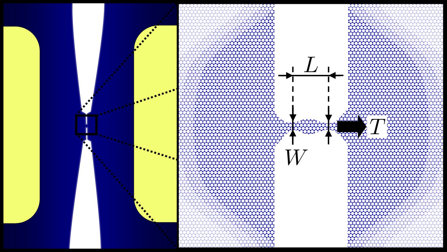
The prototypical system we consider is shown in Fig. 1. It is a tripartitioned system consisting of a central device (a graphene nanoribbon, a slit or a graphene quantum dot), contacted to mesoscopic leads made of two semi-infinite graphene half planes. The system parameters which affect the response of the system with respect to optical-like phenomena are the aperture of the contact, the typical length , and the energy dependent electron wavelength . The chirality and the electronic structure of the ribbon can also affect the conductance of the device. Yet we will show that the quantum interference effects studied here present a universal behaviour, independent of the electronic structure of the system, that present a deep analogy with phenomena that are known in subwavelength optics Ozbay ; Barnes .
Our methodology relies on an exact numerical calculation of the conductance within a tight-binding C and a Landauer quantum transport formalisms. The novelty is that the Landauer equation is solved via a new recursive numerical algorithm which reduces complex 3D/2D various shaped quantum transport devices into an effective 1D system. Here only the channels effectively contributing to the conductance are considered; the method thus allows to exactly compute the contact resistance in an efficient way.
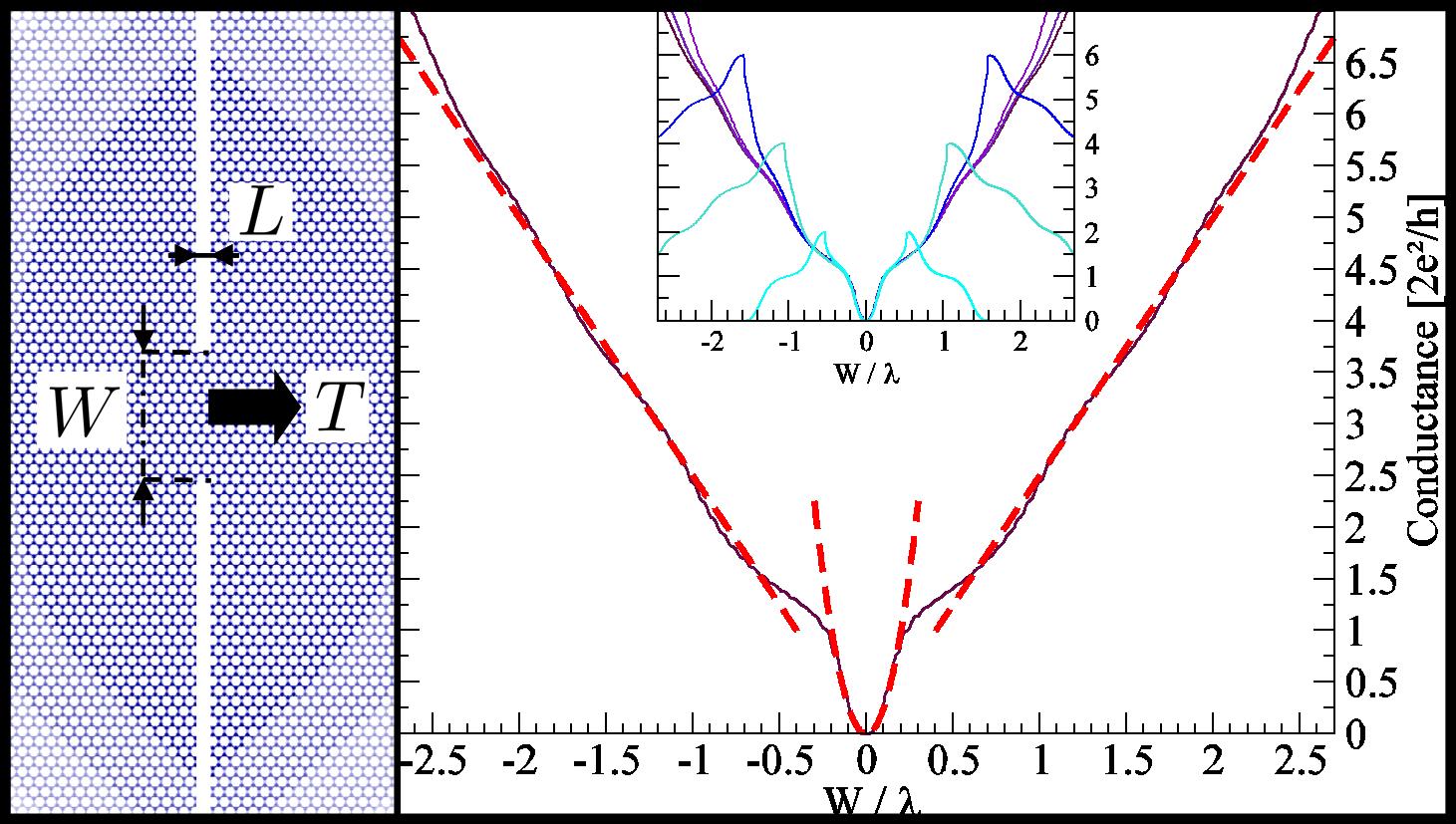
Conductance of graphene slits and diffraction - The archetype experiment showing an optical behaviour is the transmission through a hole, for example in the geometry indicated in the left panel of Fig. 2. The conductance of the slit is related to the transmission of eigenstates (or modes) through the slit. Therefoore the situation is obviously connected to the textbook experiment of diffraction by a hole. In optics depending on the hole width relative to the wavelength there are different regimes. The standard Kirchoff theory applies only in the large wavelength limit. However the phenomenon of diffraction through a subwavelength slit or through an array of such slits is central to subwavelength optics and plasmonics Ozbay ; Barnes ; Ebbesen . Analogeous results are detailed here forthe conductance of graphene slits.
Here we report the conductance of several slits that consist of a single motif, i.e. a single hexagon (the edges of the graphene half-planes being of the armchair type) but differing by the width (Fig. 2 inset). We introduce the wavelength of the incident Dirac electrons:
| (1) |
where is the Dirac electrons wavevector, is the momentum, is the energy, linearly dispersed in graphene with a Fermi velocity of ms-1 D .
We first note (Fig. 2 inset) that for all the slit widths a universal scaling occurs such that the conductance depends only on the ratio . This scaling breaks down when the wavelength is nm, that is the energy is greater than approximately eV. Indeed as shown below this scaling is intimately related to the scaling properties of the Dirac equation which is valid only in the low energy or long wavelength limit.
We then note that in the limit , the conductance is quadratic, with the conductance , while in the opposite limit , the conductance turns out to be linear with . The crossover between the two regimes occurs around . This promptly reminds of the analogy with classical optics and hence offers an immediate interpretation. We can identify two different diffraction regimes: for wavelengths , much larger than the aperture, we observe a Bethe-like diffraction regime Bethe with a slit transmitted energy proportional to the square of the aperture. On the other hand, for one has a Kirchhoff-like diffraction regime, the transmitted energy being proportional to the aperture. Thus the fact that the system does not conduct at the Dirac energy is a manifestation not of the system electronic structure, but rather of the classical optical inability of an incident wave to be transmitted through a subwavelength constriction which hence behaves like a barrier.
The explanation of both the observed diffraction patterns and of the universal scaling law comes from analogies between Maxwell equations and the Dirac equation here. Indeed, a universal scaling is also observed in ordinary optical diffraction for the slit transmitted intensity due to the scaling invariance of Maxwell equations. Here it stems from the fundamental scaling invariance of the graphene 2D Dirac equation which can be written in a dimensionless form,
| (2) |
where are the Pauli matrices, is a two component pseudo-spinor, and . The scale invariant ( dependent) form of the Dirac equation directly stems from the linear dispersion relation . This leads to the fact that the conductance undergoes a scale invariance , so it only depends from a reduced argument , .
The argument is as follows. Let us consider a system where each half plane of graphene is replaced by a ribbon of width . The symmetry axis of the ribbon is perpendicular to the slit, passing by the center of the slit. The conductance for half graphene plane is . We assume that the boundary conditions preserve the scaling, which is evidenced here by the numerical results. This is also the case for continuous type models of confinement Footnote2 . Then there is a one to one correspondence between the scattering states at wavelength ribbon width , slit width and those at wavelength , ribbon width and slit width . This means that the conductance satisfies and as a consequence .
Nanoribbons as subwavelength waveguides - Another very well-known evidence for interference effects, are the Fabry-Perot oscillations, which occur when an optical waveguide is sandwiched in between two reflecting surfaces. Several studies of subwavelength optical waveguides have shown the existence of Fabry-Perot oscillations of the transmitted intensity for an incident wave parallel to the axis of waveguide. This is for instance the case for strips in subwavelength optical metallic gratings Cavity2 or subwavelength slits in metallic screens with a finite thickness Takakura ; Suckling . In these systems the reflection at the ends of the waveguide is in fact intimately related to the diffraction by the subwavelength aperture.
In our case, the corresponding transport configuration is a metallic entity (corresponding to the optical waveguide), that we chose to be a metallic graphene nanoribbon, connected to two semi-infinite planes of graphene. Here also as discussed below the diffraction by the small apertures of the ribbon produces the reflection phenomena at the ends of the nanoribbons. Graphene nanoribbons can be realized by standard lithography techniques B ; B2 ; J . We considered a zigzag and an armchair ribbon, both chosen with a metallic character and hence an available conductance channel at the Dirac energy dresselhaus , which can thus be considered from an optics point of view as waveguides.
Calculating the conductance for both metallic nanoribbons (Fig. 3) clearly reveals a Fabry-Perot behaviour. Let us note that these oscillations exist for perfect nanoribbons but could be destroyed for example by edge defects J ; K1 ; K2 . The most evident features are large amplitude oscillations in the conductance, from maxima values of 1 to minima placed along an envelope function. These are standard Fabry-Perot oscillations of the transmittance which follow the Airy function
| (3) |
where is the phase difference after one loop in the nanoribbon. is the wavevector of the Bloch state in the infinite ribbon with energy . is the phase factor acquired at each reflection. is the length of the Fabry-Perot interferometer. is the finesse coefficient where is the reflection coefficient at each end of the nanoribbon.
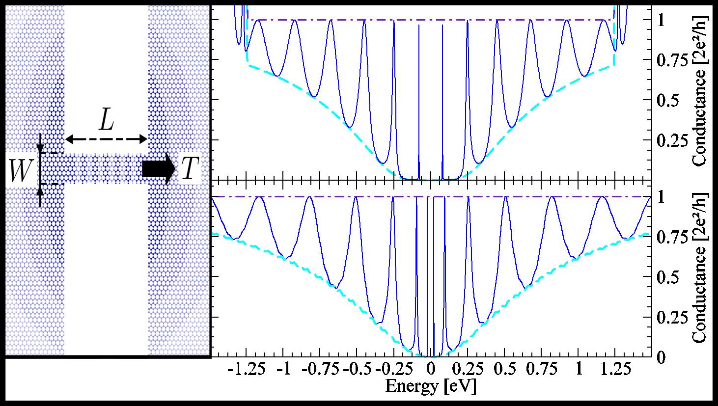
The Airy function presents maxima equal to 1 when is an integer multiple of . For sufficiently large the phase varies rapidly with energy, as compared to ; and the minima occur essentially when is maximum, that is at , and envelope along the function which independent of the size as we have numerically checked.
| (4) |
The minimum of conductance tends to zero at small energies indicating that tends to close to the Dirac energy.
The peaks full width at half maximum is such as the peaks look thin when is close to 1, and broaden when . In our case when the peaks seem to have negligible width, indicating again that close to the Dirac energy. The peaks broaden for the higher energies, indicating lower values of .
Concept of electronic diffraction barrier - The previous study on nanoribbons shows the existence of Fabry-Perot oscillations and thus a phenomenon of reflexion at each end of the ribbon characterized by a reflexion coefficient . Just as for the optical analogues this relexion phenomena is intimately connected to diffraction at the ends of the ribbon.
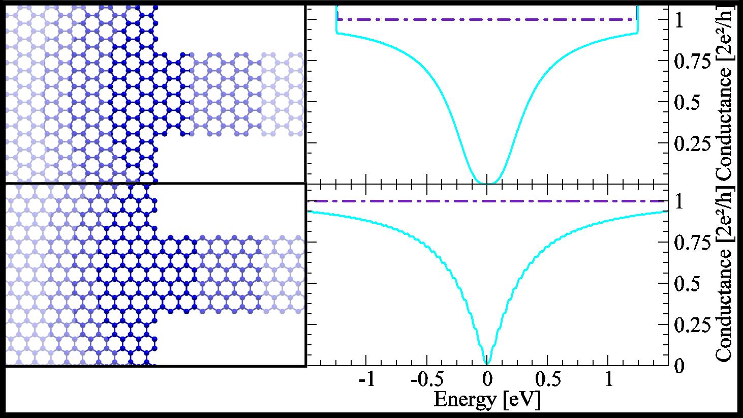
The reflexion coefficient is related to the conductance of a junction between a semi-infinite metallic ribbon and a graphene half-plane (Fig. 4) by . If there was no reflexion we would expect to observe a conductance equal to 1 quantum of conductance () (dot-dashed line in Fig. 4) in the range of the Dirac/Fermi energy. Instead, the calculated transmittance through the junction (continous line in Fig. 4) is observed to drop to zero at the Dirac energy, no matter the chirality, exactly like in slits. This means that the reflexion coefficient tends to at the Dirac energy as expected from the analysis of Fabry-Perot oscillations (see above). We have checked also that formula 4 gives the correct minima of the oscillations with calculated from the junction transmission .
Let us stress that behaviour is genuinely a manifestation of the contact resistance at the junction, which is independent of the length of the ribbon, due to its metallic character. At the opposite, in the case of non-metallic nanoribbons where confinement effects create a gap in electronic structure Berger ; Berger2 , the average resistance increases exponentially with the length of the ribbon.
The junction conductance we have calculated here is an example of the elementary electronic diffraction barrier which is at the basis of the universal behaviour observed in the devices hereby studied.
Application to quantum dots - With the concept of electronic diffraction barrier at a contact we can now analyse the conductance of standard systems of nanoelectronics i.e. quantum dots. We consider two examples that illustrate the role of geometry and the role of a chemical functionalisation of the dot .
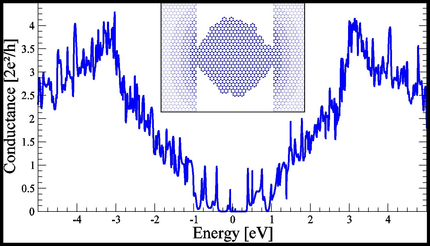
We consider first a graphene quantum dot (Fig. 5) consisting of a purposely irregular shape graphene nanostructure contacted via small apertures to the two half-planes graphene leads. From the concept of electronic diffraction barrier we expect that the quantum dot is weakly coupled to the leads when the energy of the electrons in the graphene sheet is close to the Dirac energy, i.e. when their wavelength is sufficiently large.
We note that the conductance of this system (Fig. 5) presents a maximum around eV which is the energy of the Van-Hove singularity of bulk graphene where the density of states diverges. We also note many irregular peaks superimposed to the envelope, clearly showing characteristic resonances of the quantum dot to be associated to the particular (irregular) shape. The conductance decreases when approaching to the Dirac point, which is a signature of the lowest number of available states and of a diffraction barrier at the contact constrictions.
The maximum to minimum transmission ratio between adjacent peaks is much larger in the vicinity of the Dirac energy than at other energies, a phenomena which is also observed in the nanoribbons studied previously. This is due to the two electronic diffraction barriers at the contacts which are nearly completely reflecting () at the Dirac energy. This leads to well defined states (or modes) within the quantum dot, and thus to transmission channels at well defined energies through these states.
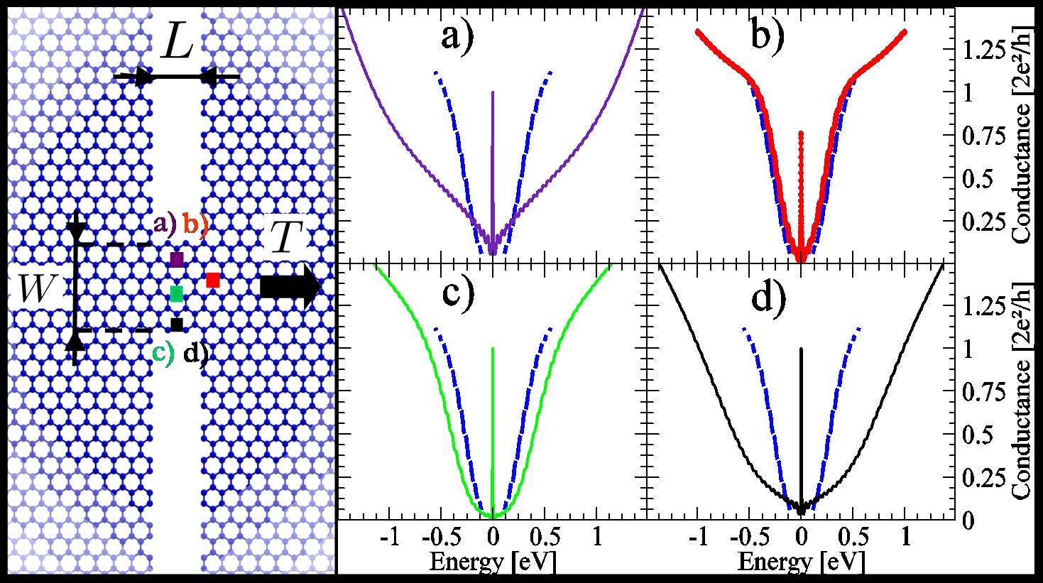
A second example is the effect of the functionalization by impurities on the response of a graphene quantum dot. Here our quantum dot is a very short graphene nanoribbon contacted by small apertures to half-plane graphene leads. This is like in the slit geometry studied above. The novelty is that now resonances in the quantum dot are induced by functionalization. A carbon atom is removed at a given position and this should mimic the effect of functionalisation by chemical entities like OH or other groups that strongly hybridize with the carbon orbitals E . Due to the specific electronic structure of graphene, functionalization of one carbon atom in the plane creates a so-called vacancy state at the zero (i.e. Dirac) energy F . This vacancy state deeply modifies the conduction properties of the constriction. Indeed Fig. 6 shows at the Dirac energy a well defined peak of conductance corresponding to the vacancy state.
When the defect is applied within the short nanoribbon, like in the positions indicated as a), c) or d) in Fig. 6, the transmission peak reaches the full value 1. The total conductance characteristics is also affected by the lateral position of the defect. A defect whose position is shifted toward the contact, as in case b) of Fig. 6, produces the conductance characteristics of the simple constriction plus a defect peak at the Dirac energy which does not reach the full quantum of conductance. The heigth of the peak lowers when shifting the defect more distant from the nanoribbon within the graphene lead.
The fact that the contacts work as diffraction barriers decouples the central device from the leads, and hence the vacancy state from the leads states. The transmission by the vacancy mode through a double barrier can be modeled by the standard Lorentzian approximation G :
| (5) |
where is the resonance energy and , where and measure the coupling of the resonant state to the leads. For a symmetric position of the functionalized atom with respect to the left and right contacts, like in the positions indicated as a), c) or d) in Fig. 6, the double barrier is symmetric. We have and the maximum transmission is one. For an asymmetric position of the functionalized atom, like in the position b) in Fig. 6, the double barrier is asymmetric and the maximum transmission is smaller than one. The maximum transmission in the peak tends to zero when the ratio tends to zero or to infinity, i.e. when shifting the defect more and more within the graphene lead.
Let us emphasize also that in a metallic nanotube functionalized by an OH group, a state (for example a bond) is removed from a conduction level and the conductance becomes 0 at the level of the removed state H . Instead, when functionalizing within diffraction barriers like in the present case, the conductance is enhanced rather than destroyed.
Let’s now discuss experimental implications of our findings on quantum dots and suggest new experiments as well as possible technological devices.
We find that the computed characteristics of the geometric quantum dot (Fig. 5) looks very similar to what has been effectively measured in a recent experiment done on a graphene quantum dot (see Ref. Geim ). The present work gives important insight in the role of difffraction to produce the electron confinement in the dot, in particular for energies close to the Dirac point.
More generally we note that the control of the characteristics of existing quantum dot is always a difficult task and the graphene quantum dot discussed here offers new possibilities. For instance, using appropriate electric gates Ensslin it is possible to adapt the wavelength of the incident and outcoming electrons in the half planes. This will modulate the characteristics of the barriers that couple the quantum dot to the leads. It is then possible to go from a small to a large barrier transparency, and thus to study a transition from a localized to a metallic regime.
Finally the functionalized graphene constriction could have applications in spintronics. Indeed, with a spin polarized defect, the quantum dot allows the production of spin polarized currents. Control over the spin of the defect by a magnetic field could provide control over the spin current providing a molecular spin valve.
To conclude our work establishes an important link between nanoelectronics and subwavelength optics, that could be experimentally tested thanks to the remarquable properties of graphene. The concept of ”electronic diffraction barrier” is central to the understanding of transport properties of subwavelength graphene nanodevices. It allowed us in particular to get insigth in the properties of quantum dots and to propose a new kind of technological device for molecular spin valves. This shows the high potential of the bridging between subwavelength optics and nanoelectronics with graphene as a constituent material.
Acknowledgements - This work has benefited from exchanges with many colleagues. We thank in particular F. Balestro, X. Blase, D. Feinberg, J. Le Perchec, L. Lévy, L. Magaud, P. Mallet, C. Naud, T. Lopez-Rios, P. Quémerais, F. Varchon, J. Y. Veuillen and W. Wernsdorfer. We also thank C. Berger & W. de Heer for a critical reading of the manuscript. Computer time has been granted by IDRIS and CIMENT/PHYNUM.
References
- (1) Datta, S. Electronic Transport in Mesoscopic Systems (Cambridge University Press, Cambridge, 1995).
- (2) Wolf, P.-E. & Maret, G. Weak localization and coherent backscattering of photons in disordered media. Phys. Rev. Lett. 55, 2696 (1985).
- (3) Cheianov, V. V., Fal’ko, V. & Altshuler, B. L. The Focusing of Electron Flow and a Veselago Lens in Graphene p-n Junctions. Science 315, 1252 (2007).
- (4) Novoselov, K. S. et al. Two-dimensional gas of massless Dirac fermions in graphene. Nature 438, 197-200 (2005).
- (5) Zhang, Y., Tan, Y.-W., Stormer, H. L. & Kim, P. Experimental observation of the quantum Hall effect and Berry’s phase in graphene. Nature 438, 201-204 (2005).
- (6) Berger, C. et al. Electronic confinement and coherence in patterned epitaxial graphene. Science 312, 1191-1196 (2006).
- (7) de Heer, W. A. et al. Epitaxial graphene. Solid State Com. 143, 92-100 (2007).
- (8) Bolotin, K. I. et al. Ultrahigh electron mobility in suspended graphene. Solid State Com. 146, 351-355 (2008).
- (9) Özyilmaz, B. et al. Electronic transport and quantum Hall effect in bipolar graphene p-n-p Junctions. Phys. Rev. Lett. 99, 166804 (2007).
- (10) Li, X., Wang, X., Zhang, L., Lee, S. & Dai, H. Chemically Derived, Ultrasmooth Graphene Nanoribbon Semiconductors. Science 319, 1229 (2008).
- (11) Ponomarenko, L. A. et al. Chaotic Dirac billiard in graphene quantum dots. Science 320, 356 (2008).
- (12) Ozbay, E. Plasmonics: Merging Photonics and Electronics at nanoscale Dimensions. Science 311, 189 - 193 (2006).
- (13) Barnes, W. L.,Dereux, A. & Ebbesen, T. W. Surface plasmon subwavelength optics. Nature 424, 824 - 830 (2003).
- (14) Wallace, P. R. The band theory of graphite. Phys. Rev. 71, 622 (1947).
- (15) Ebbesen, T. W.,Lezec, H. J., Ghaemi, H. F., , Thio, T., & Wolf, P. E. Extraordinary optical transmission through sub-wavelength hole arrays. Nature 391, 667 - 669 (1998).
- (16) Geim, A. K. & Novoselov, K. S. The rise of graphene. Nature Materials 6, 183 - 191 (2007).
- (17) Bethe, H. A. Theory of diffraction by small holes. Phys. Rev. 66, 163 (1944).
- (18) Peres, N. M. R., Castro Neto, A. H. & Guinea, F. Dirac fermion confinement in graphene. Phys. Rev. B 73, 241403(R) (2006).
- (19) Quémerais, P., Barbara, A., Le Perchec, J. & López-R os, T. Efficient excitation of subwavelength metallic gratings. J. App. Phys. 97, 053507 (2005).
- (20) Takakura,Y. Optical Resonance in a Narrow Slit in a Thick Metallic Screen. Phys. Rev. Lett. 86, 5601-5603 (2001).
- (21) Suckling,J. R et al. Finite Conductance Governs the Resonance Transmission of Thin Metals Slits at Microwave Frequencies. Phys. Rev. Lett. 92, 147401(2004).
- (22) Nakada, K., Fujita, M., Dresselhaus, G. & Dresselhaus, M. S. Edge state in graphene ribbons: Nanometer size effect and edge shape dependence. Phys. Rev. B 54, 17954 (1996).
- (23) Lin, Y.-M., Perebeinos, V. , Chen, Z. & Avouris, P. Conductance quantization in graphene nanoribbons. arXiv:0805.0035.
- (24) Mucciolo, E. R., Castro Neto, A. H. & Lewenkopf, C. H. Conductance quantization and transport gap in disordered graphene nanoribbons. arXiv:0806.3777.
- (25) Lherbier, A., Biel, B., Niquet, Y.-M., & Roche, S. Transport length scales in disordered graphene-Based materials: Strong localization regimes and dimensionality effects. Phys. Rev. Lett. 100, 036803 (2008).
- (26) Lee, Y.-S. & Marzari, N. Cycloaddition functionalizations to preserve or control the conductance of carbon nanotubes. Phys. Rev. Lett. 97, 116801 (2006).
- (27) Pereira, V. M., Guinea, F., Lopes dos Santos, J. M. B., Peres, N. M. R., & Castro Neto, A. H. Disorder Induced Localized States in Graphene. Phys. Rev. Lett. 96, 036801 (2006).
- (28) Choi, H. J., Ihm, J., Louie, S. G. & Cohen, M. L. Defects, quasibound states, and quantum conductance in metallic carbon nanotubes. Phys. Rev. Lett. 84, 2917 (2000).
- (29) Stampfer, C. et al. Tunable Coulomb blockade in nanostructured graphene. Appl. Phys. Lett. 92, 012102 (2008).