Study of the internal mechanisms of Pixelized Photon Detectors operated in Geiger-mode
Abstract
In the 1990s, a novel semiconductor photon-sensor operated in Geiger-mode was invented in Russia (Silicon PhotoMultiplier), which consists of many tiny pixels and has a single photon level sensitivity. Since then, various types of the sensor with this scheme, Pixelized Photon Detectors (PPD), have been developed in many places in the world. For instance, Hamamatsu Photonics K.K. in Japan produces the PPD as a Multi-Pixel Photon Counter.
While the internal mechanisms of the PPD have been intensively studied in recent years, the existing models do not succeeded to fully reproduce the output characteristic, such as waveforms at low temperature. We have developed a new model with the transient multiplication and quenching of the realistic avalanche process and have succeeded in reproducing the output waveform of the PPD at various temperature. In this paper, we discuss our improved model.
keywords:
PPD, Multi-Pixel Photon Counter, Silicon PhotoMultiplier, Internal mechanism, SiPM, MPPC, , , , , ,
1 Introduction
In the 1990s, a novel semiconductor photon-sensor operated in Geiger-mode was invented in Russia (Silicon PhotoMultiplier) [1, 2], which consists of many tiny pixels and has a single photon level sensitivity. Since then, various types of the sensor with this scheme have been developed in many places in the world [3]. For instance, Hamamatsu Photonics K.K. (HPK) in Japan produces a Multi-Pixel Photon Counter (MPPC) [4, 5]. Recently these devices are called as Pixelized Photon Detectors (PPD) [6].
Since the PPD has many advantages over PMTs, such as compact size, low cost, low power consumption and insensitive to magnetic field, it could be a successor to them in high energy experiments and/or in medical fields in the near future.
The particular device studied in this paper is S10262-11-025 of MPPC by HPK which has a photosensitive surface and consists of 1600 pixels in total.
We studied the basic properties of the MPPC at low temperature [7] and found that output waveform has a spike component which can not be fully explained by existing models. We introduced a new model in which the realistic avalanche process is considered and succeeded in reproducing the output waveform at various temperature.
2 Existing models of the PPD
2.1 The traditional model
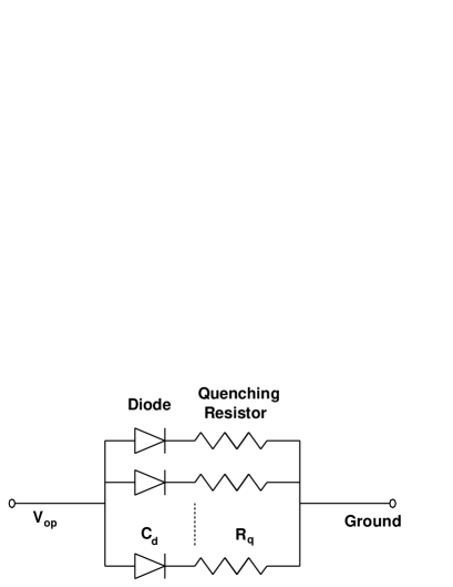
Figure 1 shows the traditionally used equivalent circuit for the PPD which explains the linearity between the gain () and the operating voltage (). The PPD has multiple pixels and each pixel consists of a diode and a quenching resistor (). The PPD is operated at a few volts higher than the breakdown voltage (), namely Geiger-mode, and the diode itself does not have the capability to terminate the avalanche process. Hence, the quenching resistor is necessary in order to decrease the voltage applied to the diode. When the current fed into the resistor is , where is , the voltage applied to the diode drops to and the multiplication stops. As a result, the gain is obtained as follows: , where is the capacitance value of the diode and the elementary electric charge.
2.2 Waveform at low temperature
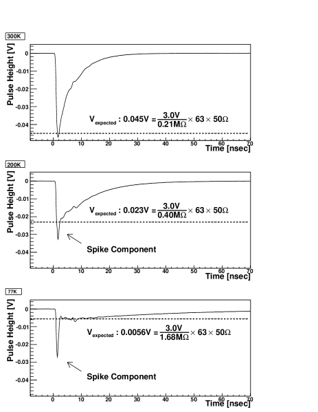
We studied the basic properties, such as waveforms, of MPPC produced by HPK at 300K, 200K and 77K [7]. The used amplifier was C5549 (bandwidth 1.5GHz) produced by HPK whose multiplication factor and input impedance are 63 and 50, respectively. Figure 2 shows the average waveform at each temperature, where is fixed at 3.0V, and a spike component is seen in the waveforms taken at 200K and 77K. Although the existence of two components has already been reported by the ITC-irst group at room temperature with a SiPM [8, 9], it is the first time to observe the sharp spike component shown in the waveform of MPPC at 77K.
can be measured from the forward current-voltage characteristics of the PPD by using the following equation: , where , and are the forward current value, the forward voltage and the number of pixels, respectively. The resistor values obtained were shown in Table 1.
The negative temperature coefficient of resistivity is due to the amorphous-like structure of poly-silicon [10] which is the main component of the quenching resistor in the MPPC.
2.3 A problem on the traditional model
Dashed lines in the Figure 2 indicate the expected pulse height () by the traditional model, which can be obtained from the following equation: , where is the multiplication factor of the amplifier and is the input impedance.
The spike component becomes much higher than at low temperature. The traditional model is thus not sufficient for explaining the output waveform of the PPD. and the measured pulse height () at each temperature are also summarized in Table 1.
| [K] | [M] | [V] | [V] |
|---|---|---|---|
| 300 | 0.21 | 0.045 | 0.047 |
| 200 | 0.40 | 0.023 | 0.033 |
| 77 | 1.68 | 0.0056 | 0.027 |
2.4 A model developed by the ITC-irst group
ITC-irst group looked into a capacitance () located between the quenching resistor and the diode as a possible reason for explaining two components. is typically in the order of 1fF [11]. Figure 3 shows its equivalent circuit proposed by them. They simplified the scheme of the multiplication and quenching and substituted a switch. is the series resistance of the diode.
As a consequence, they succeeded in reproducing the two components by tuning the parameters, such as and .

3 A new model including the avalanche process
Although the existence of the two components is explained by ITC-irst group, the avalanche process is described by the switch and the transient multiplication is not included in their model. We introduce a new model in which the realistic avalanche process is considered so as to reproduce well the output waveform.
3.1 A reproduction of the output waveforms
Our model is shown in Figure 4 and it is described by the charge of created carriers in the multiplication layer in the diode rather than by the switches of the model by ITC-irst group.

depends on the ionization rate of electrons and holes, and , which are proportional to , where is the electric field strength and is a constant [12]. We calculated the ionization rate from the interpolated values of the measurement by Grant [13]. Thus can be expressed by:
where and are the densities of electrons and holes in the diode, and are the drift velocities of each carrier, is the voltage applied to the diode and is the width of the diode. In this calculation, is fixed at .
We fixed and at , because they are saturated and remain constant in the high electric field at any temperature [14], and ignored the temperature dependence of and [15]. We calculated the electric field of the typical PPD [16] and obtained the almost uniform electric field in the multiplication layer in the diode, thus we substitute for . As a result, the equations are simplified as follows:
| (1) |
Next, the circuit equations are the following:
where is the observable current. The equation of equilibrium of the charge in the diode is calculated from and :
, and are substituted into the first equation and the following differential equation can be obtained:
| (2) |
From Eqs.(1) and (2), and are sequentially solved and the output current of the PPD can be expressed by:
For the purpose of comparison with observed current, the frequency characteristics of the used connectors, cables and amplifier have to be taken into account [17]. For our system the transmission properties are determined by the connector since it has the smallest bandwidth of all components at 1.4GHz (Suhner QLA). The bandwidths of the amplifier and the cable are 1.5GHz and 2.0GHz, respectively. Figure 5 shows the pulse distortion of our system.
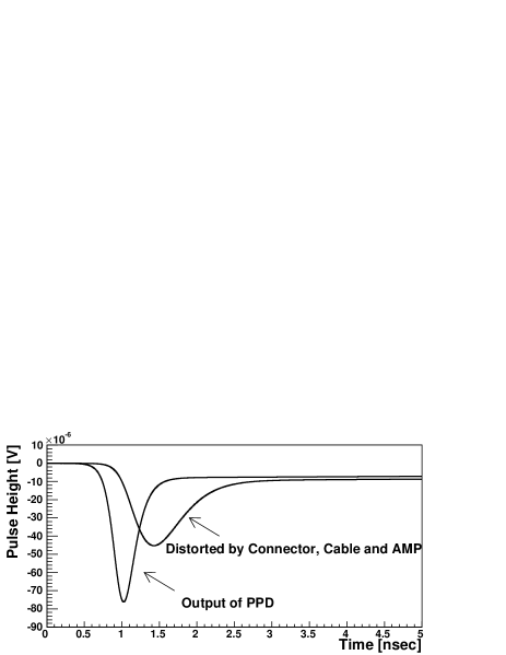
Hence, the leading and trailing edge of the spike component at 77K are characterized by the bandwidth of the connector, 1.4GHz. is already obtained as 1.68M and can be calculated from the time constant of the recovery process, [18]. In order to calibrate , we evaluate the pulse height of spike component at 77K, because it is the most sensitive to the variation of . Consequently, we can obtain as 2fF.
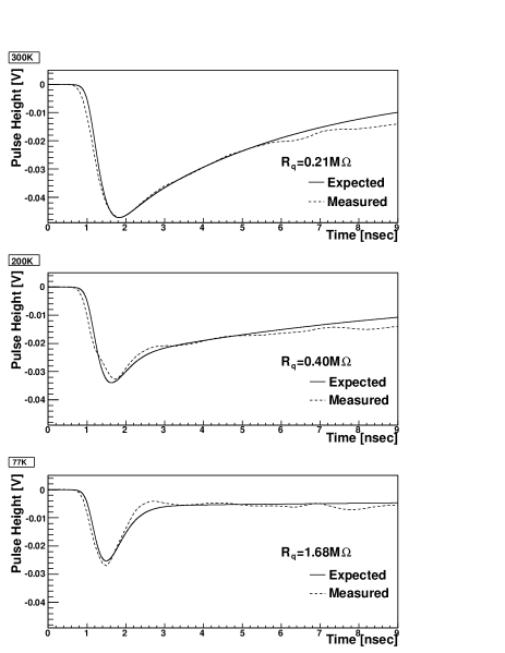
The expected and measured waveforms at each temperature are shown in Figure 6 by the solid and dashed curves, respectively. All parameters are summarized in Table 2. Note that and are calibrated from the waveform at 77K. The same values are applied to the waveform at 200K and 300K.
| [K] | [M] | [fF] | [fF] |
|---|---|---|---|
| 77 | 1.68 | 20.2 | 2 |
| 300 | 0.21 | 20.2 | 2 |
| 200 | 0.40 | 20.2 | 2 |
The waveforms in Figure 6 are the closeup view of Figure 2 and the expected waveforms compare well with the measured ones. Therefore, our model properly includes the multiplication and quenching process and reproduces the output waveform of the PPD.
3.2 A reproduction of relationship
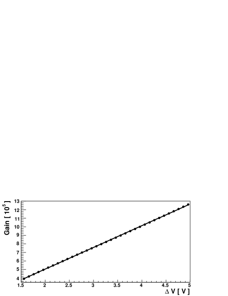
In the model by ITC-irst group, the linearity between the gain of the PPD () and is determined by the opening of the switch when drops to , which forces the termination of the avalanche process. This guarantees that the gain relationship is in accord with PPD measurements, for which the relationship is indeed linear. In our model there is no such forcing, and as such drops below . Thus, this linearity is not trivially determined. We have though calculated the relationship from the model and have in fact found it to be linear as shown in Figure 7 which is further verification of the model.
4 Conclusion
We developed a new model for a Pixelized Photon Detector (PPD), which includes the dynamical avalanche process. By calculating the circuit equations of the model, the multiplication and quenching process can be naturally incorporated as following.
The moment the avalanche process occurs, the current feeds into the capacitance and is observed as the spike component of the waveform. The leading and trailing edge of the spike component is determined by the transmission properties of the measurement system. At the same time, the avalanche multiplication begins to be suppressed by the current fed into the quenching resistor and finally quenches. After quenching, the recovery process is characterized by the time constant, , where is the capacitance value of the diode.
Furthermore we have succeeded in reproducing the observed characteristic waveforms, such as sharp spike component at 77K. The waveforms at 200K and 300K can also reproduced with and calibrated from the waveform at 77K and measured . Note that there is no variable for reproducing the waveforms at 200K and 300K.
Consequently, the model proposed in this paper makes it possible to properly incorporate the internal mechanisms of the PPD. Therefore, it should play an important role for the development of PPDs in the future.
5 Acknowledgments
The authors wish to express our deep appreciation to the KEK-DTP photon-sensor group members for their helpful discussions and suggestions. This work was supported by Grant-in-Aid for JSPS Fellows and by Grant-in-Aid for Exploratory Research from the Japan Society for the Promotion of Science (JSPS).
References
- [1] V. Golovin. Patent No. RU, 2142175, 1998.
- [2] Z. Sadygov. Patent No. RU, 2102820, 1998.
- [3] D. Renker. Geiger-mode avalanche photodiodes, history, properties and problems. Nucl. Instr. Meth., A567:48–56, 2006.
- [4] K. Yamamoto et al. Newly developed semiconductor detectors by Hamamatsu. Proceedings of International Workshop on new Photon-Detectors PD07, PoS(PD07)004.
- [5] S. Gomi et al. Development and study of the multi pixel photon counter. Nucl. Instr. Meth., A581:427–432, 2007.
- [6] C. Amsler et al. Review of particle physics. Phys. Lett., B667:1, 2008.
- [7] H. Otono et al. Study of MPPC at liquid nitrogen temperature. Proceedings of International Workshop on new Photon-Detectors PD07, PoS(PD07)007.
- [8] C. Piemonte et al. Characterization of the First Prototypes of Silicon Photomuliplier Fabricated at ITC-irst. IEEE Transaction on Nuclear Science, Vol.54, No.1:236–244, 2007.
- [9] C. Piemonte et al. A New Silicon Photomultiplier structure for blue light detection. Nucl. Instr. Meth., A568:224–232, 2006.
- [10] K. Kato et al. A Physical Mechanism of Current-Induced Resistance Decrease in Heavily Doped Polysilicon Resistors. IEEE Trans. Elec., ED-29, No.8:1156–1161, 1982.
- [11] F. Corsi et al. Modeling a silicon photomultipliers (SiPM) as a singal source for optimum front-end design. Nucl. Instr. Meth., A572:416–418, 2007.
- [12] W. Maes et al. Impact Ionization in Silicon: A Review and Update. Solid-State Electronics, Vol.33, No.6:705–718, 1990.
- [13] W.N. Grant. Electron and hole ionization rates in epitaxial silicon at high electric fields. Solid-State Electronics, Vol.16:1189–1203, 1973.
- [14] C. Jacobi et al. A review of some charge transport properties of silicon. Solid-State Electronics, Vol.20:77–89, 1977.
- [15] K. Rose et al. Temperature dependent effective ionization coefficient for Si. J. Appl. Phys., Vol.83, No.9:4988–4990, 1998.
- [16] T. Kagawa et al. Design of Deep Guard Ring for Geiger Mode Operation Avalanche Photodiode. IEICE TRANS. ELECTRON., Vol.E88-CC, No.11, 2005.
- [17] G Brianti. Distortion of Fast Pulses in Coaxial Cables Numerical Analysis and Applications. Cern Yellow Report, 65-10, 1965.
- [18] H. Oide et al. Study of afterpulsing of MPPC with waveform analysis. Proceedings of International Workshop on new Photon-Detectors PD07, PoS(PD07)008.