Current induced resistance change of magnetic tunnel junctions with ultra-thin MgO tunnel barriers
Abstract
Ultra-thin magnetic tunnel junctions with low resistive MgO tunnel barriers are prepared to examine their stability under large current stress. The devices show magnetoresistance ratios of up to 110 % and an area resistance product of down to 4.4 . If a large current is applied, a reversible resistance change is observed, which can be attributed to two different processes during stressing and one relaxation process afterwards. Here, we analyze the time dependence of the resistance and use a simple model to explain the observed behavior. The explanation is furter supported by numerical fits to the data in order to quantify the timescales of the involved phenomena.
pacs:
68.35.Dv, 72.25.-b, 73.40.GkI Introduction
The switching of a ferromagnet’s magnetization by injection of a spin polarized current (Spin Transfer Torque STT switching) is an important new phenomenon in magnetism Slonczewski (1996); Berger (1996). It enables applications such as spin torque nano-oscillators (STNO), Magnetic Random Access Memory (MRAM), programmable magnetic logic and sensors Katine and Fullerton (2008) using the tunneling magnetoresistance (TMR) effect Moodera et al. (1995); Miyazaki and Tezuka (1995); Butler et al. (2001). The conventional switching scheme of field pulses generated by current lines requires large currents and is not scalable, which led to alternatives such as heat assisted Prejbeanu et al. (2007) or the already mentioned STT switching Katine et al. (2000). In state-of-the-art MgO based magnetic tunnel junctions (MTJs), STT requires current densities of about Sun (2006). This leads to a bias voltage of about , if the area-resistance products are in the order of .
Individual STNOs are strongly limited in their output power. This deficiency has to be overcome in order to exploit the benefits of current-tunable narrow-linewidth microwave generation for future application. Although an array of coupled oscillators may offer a path to higher power output Kaka et al. (2005), the individual STNOs are envisioned to be MTJ-based and operating close to the degradation current limit Katine and Fullerton (2008); Nazarov et al. (2008). Please note that STNOs are operated at direct currents in contrast to pulsed currents in the case of MRAMs.
A constant trend to reach lower area resistance products forced the fabrication of MTJs with barriers as thin as 10 . Further reduction of the tunnel barrier thickness is becoming more and more challenging. Recently, reversible resistance changes and an atypical temperature dependence of the resistance were observed in thin MTJs when reaching current densities of – Ventura et al. (2005a). These resistance changes do not depend on the relative orientation of the magnetic layers Ventura et al. (2005a) and are attributed to electromigration in nano-constrictions of the insulating barrier Ventura et al. (2005b); Ventura et al. (2006). Two opposite relaxation processes were found suggesting two independent mechanisms acting simultaneously inside the MTJs Ventura et al. (2005b).
Here, we study the effect of current stressing on ultra-thin MgO barriers. In these devices, resistance changes take place at a current density of about . This shows that further reduction of the STT switching currents is crucial in order to achieve reliable operation of STT-MTJ based devices. We distinguish two effects during the current stress and one relaxation process. Furthermore, numerical fits to the experimental data are presented.
II Results
The TMR systems with low resistive MgO barriers is sputter deposited in a Singulus TIMARIS II tool. The film sequence is Ta 3/Cu-N 90/Ta 5/Pt-Mn 20/Co-Fe 2/Ru 0.75/ Co-Fe-B 2/MgO 1.3/Co-Fe-B 3/Ta 10/Cu 30/Ru 7 (all values in nm). The composition of the compounds is: , and . Elliptical TMR elements with sizes in the range of to are prepared by e-beam lithography in combination with ion beam etching. By applying different Ar pressures during MgO deposition two sample sets with an area-resistance product of (set 1) and (set 2) are produced.
All measurements are performed using a constant voltage source at room temperature. By applying a voltage in the range of to the samples are stressed by a current density of 1 – 10. A magnetic field of provides a stable parallel/ anti-parallel orientation of the magnetic layers during the measurements. The resistance is monitored at a read-out voltage of with a rate of in order to overcome non-linear -contributions and thermal drifts related with heating processes (heating rates due to current load have typical time constants well below 1 ns Ventura et al. (2007)). Each measurement is performed on an individual element which was not stressed before. This is necessary since the properties of the barrier may change irreversibly by the stressing.
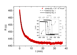
Figure 1 shows the MTJ resistance upon stressing with positive voltage polarity (electrons flow from the bottom to the top electrode). The area-resistance product is . The inset shows the magnetic minor loops before (black) and after (gray) stressing exhibiting TMR ratios of the junction of 104 % and 108 % at 20 mV, respectively. This increase in TMR gives evidence, that the barrier itself does not degrade during current stressing. As the device is stressed by one can see a decay of the resistance with time, although the films had been annealed for at prior to patterning. The initial resistance of is reduced reaching a saturation resistance of within . Numerically, the measured time dependence of the resistance can be fitted with moderate quality by an exponential function:
| (1) |
with . This would represent a process characterized by a decay time of and leads to the dashed line in Fig. 1 as will be further discussed below.
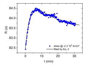
Stressing the MTJs with currents of the negative polarity leads to a substantially different response shown in Fig. 2. First, the resistance rapidly increases from to , followed by a slow decay. No saturation of the resistance can be seen within the measured time range.
Thus at least two processes are involved: A fast, polarity dependent resistance change followed by a slow resistance decrease for both polarities:
| (2) |
with () for positive (negative) polarity and for both polarities. These two exponential decays of different sign give a very good fit to the data of Fig. 2 (solid line) with and . Looking back to Fig. 1 the fast process might be hidden in the decrease because the sign depends on the polarity of the applied voltage: Two exponential decreases would lie on top of each other. In fact with Eq. 2 a better fit to the data of Fig. 1 can be obtained (solid line). In this case, however, the fit parameters and are strongly correlated and can not be used for a quantitative analysis.
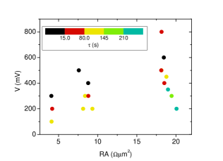
The dependence of the time constant (Fig. 1, dashed line) on the product of the junctions is shown in Fig. 3 for different positive stressing voltages. For increasing voltage a decrease in is observed. At the same time, for a given voltage, increases with increasing product.
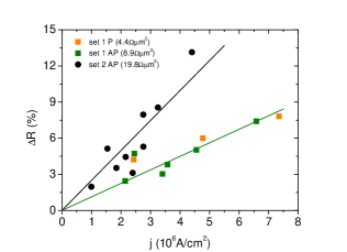
Figure 4 shows the current induced resistance variation as a function of the current density. A decrease of the resistance can be seen reaching 13 % at a current density of for sample set 2. For sample set 1 is reduced by a factor of approximately 0.45 due to the lower . This can be seen from Fig. 4 where the black line shows a linear fit to the data of sample 2 and the green line is generated by changing the slope of the black line by the ratio which is to for the antiparallel state. In contrast to this, the magnetic orientation of the electrodes (compare green and orange squares) produces no significant differences. This leads to the conclusion that the current density and not the electric field is the main parameter that determines .
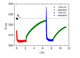
If we investigate the relaxation of the resistance, i. e. the resistance change after the current stress is released, one can reveal a third process involved. The red curve in Fig. 5 is equivalent to the plot shown in Fig. 1, the blue curve is equivalent to the plot in Fig. 2. The green curve in Fig. 5 illustrates the relaxation process: If no large voltage/ current is applied (20 mV), the resistance slowly reaches the initial level . This can also be fitted with an exponential function with typical relaxation times of 100 min.
III Discussion
For the interpretation of the data, one has to consider that the resistance of a (magnetic) tunnel junction is governed by the barrier thickness and the barrier height . This relationship can be described by Brinkman’s equation Brinkman et al. (1970). For barrier height (0.5 – 3.5 eV) and thickness (1 – 1.5 nm) that correspond to our junctions, the Brinkman equation can be reduced to
| (3) |
where and are constants. Thus, the resistance changes as given by Eq. 1 could be explained by a variation of as well as .
If we assume that the effective barrier thickness changes by a certain fraction with a nominal thickness of , Brinkmans’s equation leads to , if the resistance change is about 5 %. For a change of , a resistance change of 5 % leads to . Thus very small changes in the barrier characteristics can lead to the observed resistance changes. Provided small changes of or results in a linear approximation of Eq. 3 and the experimental findings (Eq. 1) lead to an exponential function for either or as well.
Since the layer stack is symmetric (CoFeB/ MgO/ CoFeB), the same resistance change for positive and negative bias is expected. The symmetry break is induced by the sequence of preparation. The lower ferromagnet is more likely to be contaminated with oxygen Read et al. (2007), because the MgO is deposited on top of the ferromagnet by rf-sputtering from an MgO target. This oxygen on top of the ferromagnet can act as an additional barrier Zhang et al. (2003) and also lead to oxygen deficiencies in the lower part of the tunnel barrier. Also the effective barrier height is modified by the presence of oxygen vacancies Gibson et al. (1994); Mather et al. (2006).
Therefore, a possible explanation for the observed behavior is a small displacement of these oxygen vacancies/ defect atoms driven (fast) in the direction of the electron flow increasing or decreasing the effective thickness of this layer (electromigration) Ventura et al. (2006) and (slow) by thermal activation. These processes are reversible since the atoms can slowly fall back into their initial positions of lower energy once the current is switched off.
IV Summary
In summary, we investigate magnetic tunnel junctions with MgO barriers with magnetoresistance ratios of up to 110 % and area-resistances of around 10 . The low resistance of these devices allow us to drive large currents trough the structures, which is necessary for use in spin transfer torque memory or logic cells. We observe three reversible resistance changes of the junctions: One fast, polarity dependent term that could be associated with electromigration. One slower, polarity independent term active during current stress, that is suggested to be of thermal origin. Finally, a very slow relaxation takes place when the current stress is released, which also can be explained by thermally activated diffusion.
Acknowledgments
The authors gratefully acknowledge Singulus Technologies for providing the samples. P. K. is supported by the Deutsche Forschungsgemeinschaft (DFG) through Schwerpunktprojekt 1133. X. K. is supported by the DFG within Grant No. RE 1052/16-1.
References
- Slonczewski (1996) J. Slonczewski, J. Magn. Magn. Mater 159, L1 (1996).
- Berger (1996) L. Berger, Phys. Rev. B 54, 9353 (1996).
- Katine and Fullerton (2008) J. Katine and E. E. Fullerton, J. Magn. Magn. Mat. 320, 1217 (2008).
- Moodera et al. (1995) J. S. Moodera, L. R. Kinder, T. M. Wong, and R. Meservey, Phys. Rev. Lett. 74, 3273 (1995).
- Miyazaki and Tezuka (1995) T. Miyazaki and N. Tezuka, J. Magn. Magn. Mater. 139, 231 (1995).
- Butler et al. (2001) W. H. Butler, X.-G. Zhang, T. C. Schulthess, and J. M. MacLaren, Phys. Rev. B 63, 054416 (2001).
- Prejbeanu et al. (2007) I. L. Prejbeanu, M. Kerekes, R. C. Sousa, H. Sibuet, O. Redon, B. Dieny, and J. P. Nozières, J. Phys.: Condens. Matter 19, 165218 (2007).
- Katine et al. (2000) J. A. Katine, F. J. Albert, R. A. Buhrman, E. B. Myers, and D. C. Ralph, Phys. Rev. Lett. 84, 3149 (2000).
- Sun (2006) J. Z. Sun, IBM J. Res. Dev. 50, 81 (2006).
- Kaka et al. (2005) S. Kaka, M. R. Pufall, W. H. Rippard, T. J. Silva, S. E. Russek, and J. A. Katine, Nature 437, 389 (2005).
- Nazarov et al. (2008) A. V. Nazarov, K. Nikolaev, Z. Gao, H. Cho, and D. Song, J. Appl. Phys. 103, 07A503 (2008).
- Ventura et al. (2005a) J. Ventura, J. B. Sousa, Y. Liu, Z. Zhang, and P. P. Freitas, Phys.Rev. B 72, 094432 (2005a).
- Ventura et al. (2005b) J. Ventura, J. Araujo, F. Carpinteiro, J. Sousa, Y. Liu, Z. Zhang, and P. Freitas, J. Magn. Magn. Mater. 290-291, 1067 (2005b).
- Ventura et al. (2006) J. Ventura, J. P. Araújo, J. B. Sousa, Y. Liu, Z. Zhang, and P. Freitas, IEEE Trans. Nanotech. 5, 142 (2006).
- Ventura et al. (2007) J. Ventura, A. Pereira, J. Araujo, J. Sousa, Z. Zhang, Y. Liu, and P. Freitas, J. Phys. D: Appl. Phys. 50, 5819 (2007).
- Brinkman et al. (1970) W. F. Brinkman, R. C. Dynes, and J. M. Rowell, J. Appl. Phys. 41, 1915 (1970).
- Read et al. (2007) J. C. Read, P. G. Mather, and R. A. Buhrman, Appl. Phys. Lett. 90, 132503 (2007).
- Zhang et al. (2003) X.-G. Zhang, W. H. Butler, and A. Bandyopadhyay, Phys. Rev. B 68, 092402 (2003).
- Gibson et al. (1994) A. Gibson, R. Haydock, and J. P. LaFemina, Phys. Rev. B 50, 2582 (1994).
- Mather et al. (2006) P. G. Mather, J. C. Read, and R. A. Buhrman, Phys. Rev. B 73, 205412 (2006).