Wide-angle perfect absorber/thermal emitter in the THz regime
Abstract
We show that a perfect absorber/thermal emitter exhibiting an absorption peak of 99.9% can be achieved in metallic nanostructures that can be easily fabricated. The very high absorption is maintained for large angles with a minimal shift in the center frequency and can be tuned throughout the visible and near-infrared regime by scaling the nanostructure dimensions. The stability of the spectral features at high temperatures is tested by simulations using a range of material parameters.
pacs:
44.40.+a,78.20.CiSince the beginning of the last century it is known that a perfect thermal emitter follows Planck’s law of black-body radiationPlanck (1901). Realistic structures, however, generally do not follow Planck’s law, but exhibit a smaller emission. The properties of these emitters strongly depend on the materials and their shapes. From the absorption spectra of a structure the emission properties can be deduced since Kirchhoff’s law directly relates the absorption with the emissivity. The emission is then determined by multiplying the emissivity with the black-body radiation spectrum. Using Photonic CrystalsFleming et al. (2002); Chan et al. (2006); Han et al. (2007)it has been shown that this approach is also valid for periodically structured materials. For a number of applications such as thermo-photovoltaic converters, it is necessary to control the spectral properties to achieve, e. g., selective emitters in a narrow frequency band corresponding to the band gap of solar cellsSai and Yugami (2004); Sai et al. (2005). In the case of structured metallic surfaces, the changes in the emission spectra are based on surface waves coupled to the external radiation through the periodic surface.Greffet et al. (2002); Laroche et al. (2006, 2005) Alternatively, microcavity resonances can also be used to create narrow band thermal radiation.Maruyama et al. (2001); Celanovic et al. (2005) Unfortunately, most of the recent designsLaroche et al. (2006); Tao et al. (2008)for perfect absorbers/emitters only work for one incident angle and one polarization. So, there is a need for wide-angle perfect absorber/emitter nanostructures. In this paper, we suggest a structure which exhibits a large absorption in the THz regime for a wide range of angles with respect to the surface. We show that the absorption characteristics are maintained even if the uncertainties in the estimated changes in the material parameters, due to high temperatures, are considered. The proposed structure can be easily manufactured with today’s planar micro-fabrication techniques. We also comment on the impact of deviations in the geometrical parameters caused by fabricational tolerances. The small size of the structure, in comparison to the wavelength together with the relatively straightforward fabrication, allows for easy integration into various devices, such as perfect thermal emitters, perfect absorbers, bolometers, and very effective light extraction LEDs.
The suggested structure is shown in Fig. 1. It consists of a metal back-plate (black) with a thickness larger than . This is much larger than the typical skin depth in the THz regime and avoids transmission through the structure. In this case the reflection is the only factor limiting the absorption. The thickness of the back-plate can be adjusted to the specific needs of the final application, e. g., to obtain good heat transport to sensors or to obtain a better stability. On top of the metal plate a spacer layer of Silicon-Nitride SiN is deposited with a thickness . The structure is terminated by an array of metallic stripes with a rectangular cross-section. Their arrangement is described by a lattice constant, , and their shape is given by a width, , and a thickness, . In this setup a strong resonance with a large field enhancement in the dielectric spacer layer and in between the stripes can be obtained, as will be shown later. Adjusting the size of the metal stripes on the top, the coupling to this resonance can be tuned and the reflection can be minimized.
\psfrag{myLattice}[l][l]{\Large$\mathrm{a}$}\psfrag{myTheta}[l][l]{\Large$\theta$}\psfrag{myWireWidth}[l][l]{\Large$\mathrm{W}_{w}$}\psfrag{myWireHeight}[l][l]{\Large$\mathrm{W}_{t}$}\psfrag{myDielectricHeight}[l][l]{\Large$\mathrm{D}_{t}$}\includegraphics[width=213.39566pt]{fig1}
Due to the scalability of Maxwell’s Equations, in principle, the structure can be simulated using dimensionless units by dividing all sizes by the lattice constant and using as frequency. However, the Drude model used to describe the metal requires frequencies in and therefore the lattice constant must be assigned in the simulation. If a shift in the frequencies of the spectral features by adjusting the lattice constant is intended, a new simulation must be done since changes in the dielectric constant would not be considered.
In the simulation frequency-dependent material parameters are required. We calculate them using standard methods and adjust their values to take into consideration the high temperatures. The Tungsten parts (plate and stripes) are described by a Drude model
with the plasma frequency and the collision frequency at room temperature.M. A. Ordal, L. L. Long, R. J. Bell, S. E. Bell, R. R. Bell, R. W. Alexander and C. A. Ward (1983) In order to account for the higher temperatures, we use an increased value for the collision frequency. Since the resistivity of Tungsten increases linearly with temperature, a linear dependence of the collision frequency is assumed, leading to an estimated increase of the collision frequency by a factor of 3–5 (). The plasma frequency is assumed to be constant. The simulations are repeated for several values of the collision frequency () to ensure the stability of the emission spectra in a wide range.
The index of SiN depends on the actual fabrication processPiccirillo and Gobbi (1990); Jun et al. (1999); Lee et al. (1999) and shows a strong wavelength dependence below , but is roughly constant for longer wavelengths until about .Ravindra et al. (1998) For our simulation we use experimental values for room temperature obtained from Sandia National LabEl.Kady and fitted a Cauchy model for dielectrics in the infrared to calculate the required values. In order to account for temperature increase, we assume a linear temperature dependence as found, e. g., in SilicaMcLachlan and Meyer (1987) and add a constant value () to the imaginary part of the experimental data. Again, we perform several simulations with different values of the imaginary parts of SiN (0.05, 0.1, 0.15, 0.2) for comparison.
For the simulations we use our own implementation of a Fourier-Modal method with a scattering matrix approach, also known as Rigorous-Coupled Wave Analysis (RCWA).Moharam and Gaylord (1981); Whittaker and Culshaw (1999) Special care is taken in use of the correct Fourier-factorization rules to ensure a fast convergence.Li (1996)This approach assumes incoming plane waves onto a periodic surface defined by the dimensionless frequency and the angle to the surface normal (Fig. 1). For the material parameters the frequency is calculated using a fixed lattice constant of =. The absorption is determined by subtracting the total reflection of all diffraction orders given by the individual Poynting vectors. The transmission is on the order of the numerical error. By Kirchoff’s Law the absorption equals emissivity and the emission can be calculated by multiplying the absorption with the black-body radiation, even in the case of structured materials.Chan et al. (2006)
To confirm the results and to study the field distributions/energy flow and resistive heating, we use the commercially-available finite-element-based program, Multiphysics, by Comsol with periodic boundary conditions in the direction parallel to the surface. In this case the absorption is determined by . This program is also used to determine possible eigenmodes and their corresponding complex eigenfrequencies. In this simulation, the material parameters are set to the values at the resonance frequency.
For wide-angle absorption in a small frequency window, the center frequency of the absorption peak should not shift for oblique incoming plane waves at different angles. It was shown before that Tungsten microcavities can exhibit a weak angular dependence,Sai et al. (2003); Kusunoki et al. (2004) however, the angular range and maximum absorption both are smaller than in our case. The additional dielectric layer offers the possibility to optimize the cavity geometry and the coupling to it lead to a substantial improvement. We find that the most important criteria for obtaining a very weak angular dependence is to avoid coupling to propagating diffraction orders. In the simulations we choose a lattice constant of =, so that the first negative diffraction order at large angles () is given by corresponding to . Any absorption peak at higher frequencies couples to several reflected diffraction orders and shows a strong angular dispersion at the corresponding frequency/angle combination. For a structure with the parameters given in Fig. 1, we find a strong absorption peak for perpendicular incidence fulfilling the above criteria. The corresponding reflection and absorption spectra are shown in Fig. 2.
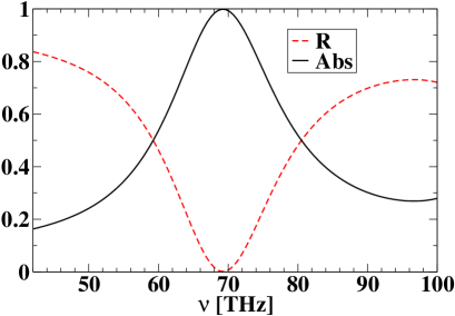
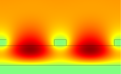
The obtained absorption peak has a center frequency of = with a half-width at half-maximum of corresponding to 14.8% of the center frequency. Simulations with Multiphysics showed, the field is able to couple into the dielectric layer in contrast to regions outside the resonance. A strong enhancement of the electric field can be found in the region between the metallic stripes mostly located in the dielectric (Fig. 3). Numerically, we find an eigenmode showing the same field pattern at an eigenfrequency of (real part of the complex eigenfrequency). In this simulation the material parameters are fixed to the values at . Changing the thickness of the metal plate or the air space in front of the structure changes the eigenfrequency by less than , once the air part in front of the structure is chosen large enough. Although losses in the dielectric layer occur due to the imaginary part, the energy flow described by the Poynting vector reveals that the main absorption takes place at the surface of metallic back-plate and the rear side of the metal stripes.
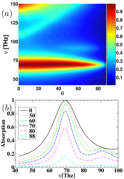
If the structure is used as a perfect absorber, e. g., in sensor applications, it is important to absorb as much of the radiation as possible, independent of the direction of incidence. In Fig. 4 we show the angular dispersion of the peak together with the spectra for several angles. For angles up to the peak becomes slightly narrower and the center frequency increases by , but the maximum absorption is above 99.7%. For larger angles the peak starts to drop, but is still above 80%, even for waves impinging on the structure with an angle of . In Fig. 4(a), two additional absorption peaks at higher frequencies are visible. Both peaks are caused by resonant modes in the dielectric as well, but their angular dependence shows a very strong dispersion. If the parameters are chosen so that the lowest peak has a higher center frequency (above 75THz for the given lattice constant), it shows a weak angular dispersion until the starts propagating and then the absorption vanishes quickly.
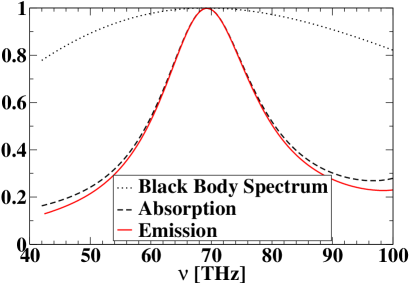
Finally, we compare the emission properties of our structure with a regular black-body emitter in Fig. 5. We plot the black-body emission using Planck’s law at a temperature of 1176K, so the maximum of the emission corresponds to the center frequency of the absorption peak. The emission of the structure given by the product of the emissivity and the black-body radiation is also plotted in Fig. 5 as a solid line. The combined effect of the two aspects suppresses the sides of the peak even stronger, so a selective emission is achieved.
For these high temperatures, the material parameters are not known exactly and must be estimated. Since estimates are always a possible source of errors, we ensured that the spectral properties exist in a wide range of parameters. We tested the results for different adjustments in the collision frequency of Tungsten (=13, 50, 100THz) and the imaginary part of the SiN dielectric (0.05, 0.1, 0.15, 0.2). For all combinations of these parameters, the absorption reaches values of 93% or more, except for the case with and = for which only 82% are achieved. The center frequency of the absorption peak remains unchanged. However, an increase in the imaginary part of SiN leads to an broadening of it. In general, an increase in the collision frequency allows for a wider range of possible adjustments in the imaginary part of the SiN.
Although we do not present the data in this paper, we also conducted several simulations to determine the sensitivity of the absorption peak to fabricational tolerances. In this study, we varied all 3 parameters (, , ) by individually and combined. In all cases an absorption of more than 98,8% was obtained. Wider (narrower) stripes lead to a small increase (decrease) in the frequency of less than . For thicker stripes, the coupling became weaker and the absorption dropped by 1%. Changes in the thickness of the dielectric layer caused the strongest change in the absorption spectra, shifting the center frequency of the peak by about . Since the field was concentrated mainly in this area, deviations in the spacer thickness changed the effective size of the cavity and, therefore, the frequency of the cavity mode. This makes it important to control the thickness of the dielectric layer very precisely in the fabrication process.
In summary, we presented a design for a perfect absorber/thermal emitter with a very high absorption peak over a wide range of angles. We demonstrated that the absorption peak is stable with respect to the estimated changes in the material parameters at high temperatures. We also studied the impact of deviations in the geometry caused by fabricational tolerances. From this it can be expected that the spectral features are also present in realistic samples. Since the structure can be built with planar fabrication techniques, it offers an interesting approach to wide angle perfect absorbers/emitters. First studies using a lattice constant of several showed that it is possible to obtain similar effects also for frequencies in the GHz range. Due to the wide angular absorption this can offer a new way to avoid reflections in microwave experiments with an easy-to-build structure on length-scales smaller than the wavelength.
M.D. gratefully acknowledges financial support from the Alexander-von-Humboldt Foundation (Feodor-Lynen Program). Work at Ames Laboratory was supported by the Department of Energy (Basic Energy Sciences) under contract No. DE-AC02-07CH11358. This work was partially supported by the office of Naval Research (Award No. N0014-07-1-0359).
References
- Planck (1901) M. Planck, Annalen der Physik 309, 553 (1901).
- Fleming et al. (2002) J. G. Fleming et al., Nature 417, 52 (2002); S. Y. Lin et al., Appl. Phys. Lett. 83, 380 (2003a); Opt. Lett. 28, 1909 (2003b).
- Chan et al. (2006) D. L. C. Chan, M. Soljačić, and J. D. Joannopoulos, Phys. Rev. E 74, 036615 (2006).
- Han et al. (2007) S. E. Han, A. Stein, and D. J. Norris, Phys. Rev. Lett. 99, 053906 (2007).
- Sai and Yugami (2004) H. Sai and H. Yugami, Appl. Phys. Lett. 85, 3399 (2004).
- Sai et al. (2005) H. Sai, Y. Kanamori, K. Hane, and H. Yugami, J. Opt. Soc. Am. A 22, 1805 (2005).
- Greffet et al. (2002) J.-J. Greffet, R. Carminati, K. Joulain, J.-P. Mulet, S. Mainguy, and Y. Chen, Nature 416, 61 (2002).
- Laroche et al. (2006) M. Laroche, R. Carminati, and J.-J.Greffet, Phys. Rev. Lett. 96, 123903 (2006).
- Laroche et al. (2005) M. Laroche et al., Opt. Lett. 30, 2623 (2005).
- Maruyama et al. (2001) S. Maruyama, T. Kashiwa, H. Yugami, and M. Esashi, Appl. Phys. Lett. 79, 1393 (2001).
- Celanovic et al. (2005) I. Celanovic, D. Perreault, and J. Kassakian, Phys. Rev. B 72, 075127 (2005).
- Tao et al. (2008) H. Tao et al., Opt. Express 16, 7181 (2008); N. I. Landy et al., Phys. Rev. Lett. 100, 207402 (2008).
- M. A. Ordal, L. L. Long, R. J. Bell, S. E. Bell, R. R. Bell, R. W. Alexander and C. A. Ward (1983) M. A. Ordal, L. L. Long, R. J. Bell, S. E. Bell, R. R. Bell, R. W. Alexander and C. A. Ward, Appl. Opt. 22, 1099 (1983).
- Piccirillo and Gobbi (1990) A. Piccirillo and A. L. Gobbi, Journal of The Electrochemical Society 137, 3910 (1990).
- Jun et al. (1999) B.-H. Jun, J. Lee, D.-W. Kim, T.-H. Sung, B.-S. Bae, and K. No, J. Mater. Res. 14, 995 (1999).
- Lee et al. (1999) C. C. Lee, H. L. Chen, J. C. Hsu, and C. L. Tien, Appl. Opt. 38, 2078 (1999).
- Ravindra et al. (1998) N. Ravindra, S. Abedrabbo, W. Chen, F. Tong, A. Nanda, and A. Speranza, Semiconductor Manufacturing, IEEE Transactions on 11, 30 (1998).
- (18) I. El.Kady, private communication.
- McLachlan and Meyer (1987) A. D. McLachlan and F. P. Meyer, Appl. Opt. 26, 1728 (1987).
- Moharam and Gaylord (1981) G. G. Moharam and T. K. Gaylord, J. Opt. Soc. Am. 71, 811 (1981).
- Whittaker and Culshaw (1999) D. M. Whittaker and I. S. Culshaw, Phys. Rev. B 60, 2610 (1999).
- Li (1996) L. Li, J. Opt. Soc. Am. A 13, 1870 (1996); J. Opt. Soc. Am. A 14, 2758 (1997).
- Sheng and He (2002) L. Sheng and S. He, J. Opt. Soc. Am. A 19, 1021 (2002).
- Sai et al. (2003) H. Sai, Y. Kanamori, and H. Yugami, Appl. Phys. Lett. 82, 1685 (2003).
- Kusunoki et al. (2004) F. Kusunoki, T. Kohama, T. Hiroshima, S. Fukumoto, J. Takahara, and T. Kobayashi, Jap. J. of Appl. Phy. 43, 5253 (2004).