Photo-current and photo-voltage oscillations in the two-dimensional electron system: screening and ”anti-screening” of a potential profile
Abstract
We observe in state-of-the-art GaAs based 2D electron systems microwave induced photo-current and photo-voltage oscillations around zero as a function of the applied magnetic field. The photo-signals pass zero whenever the microwave frequency is close to a multiple of the cyclotron resonance frequency. They originate from built-in electric fields due to for instance band bending at contacts. The oscillations correspond to a suppression (screening) or an enhancement (”anti-screening”) of these fields by the photo-excited electrons.
pacs:
72.20.Fr, 72.20.My, 73.40.KpThe strong current interest in the photo-response of the 2D electron system (2DES) exposed to microwaves was triggered by the discovery, at small perpendicular magnetic fields, of microwave induced oscillations in the magnetoresistivity Zudov1 ; Ye ; Mani ; Zudov2 and magnetoconductivity Zudov3 with minima that even drop all the way down to zero. Numerous theoretical models have been put forward to account for the oscillatory behavior. The two most prominent examples are the establishment of an oscillating non-equilibrium electron energy distribution function (NEDF) Dorozh1 ; Dmitriev1 and the scattering assisted displacement (SAD) of photo-excited electrons against or along the Hall electric field depending on the ratio between the circular microwave frequency and the electron cyclotron frequency Ryzhii1 ; Durst . The second mechanism was first treated theoretically in 1970 in Ref. Ryzhii1 well before the experimental discovery of the microwave induced resistance oscillations. It was predicted that this mechanism also gives rise to an oscillating photo-current. The main research thrust both experimentally and theoretically has however been the influence of the microwave radiation on the sample resistance. A few exceptions exists where other measurable quantities were addressed such as for instance the photo-voltage Willett ; Bykov and the electron compressibility Vavilov .
Here, we investigate the photo-signals in two geometries. The first one contains alloyed contacts at the perimeter (external contacts) as well as inside (internal contacts) the mesa. Strong magneto-oscillations crossing zero are observed in both the photo-current and voltage when measured between an internal and an external contact. In the second geometry, capacitively coupled contacts have been used to pick-up the oscillating photo-signal and to tune the potential profile with a gate voltage. The oscillations apparently come about because of the existence of built-in electric fields within the sample.
Experiments were carried out on samples produced from three different wafers A, B and C with electron densities , , and and with zero field electron mobilities , , and . While samples A and C were measured in the dark, sample B reached these characteristics after illumination with a red LED. Samples A and B (Fig. 1) consisted of a long and wide Hall bar with three voltage probes on either side of the bar and source and drain contacts at the ends. In addition, a set of 9 square shaped ohmic contacts with a side length of was fabricated within the mesa. These internal contacts were arranged in a matrix. The distance in between two rows was equal to , while columns were separated by . All contacts were made by alloying evaporated Ni/Ge/Au. The microwave induced DC photo-current was measured with a current amplifier and the photo-voltage with a precision voltmeter. The results were also verified with a lock-in technique for modulation of the incident microwave. For these lock-in measurements the photo-current was converted to a voltage by measuring either across a small resistor or the secondary coil of a transformer whose primary winding carried the induced photo-current. The second geometry in Fig. 1 was fabricated on sample C and consisted of a single ohmic contact touching the sample perimeter and two gates making up a Corbino geometry. The diameter of the inner circular gate was , while the inner and outer diameter of the annular gate were and . The incident radiation with amplitude modulation induces a displacement (capacitive) current at the modulation frequency due to charging of the capacitors which form between the gates and the 2DES (for a schematic of the measurement configuration see Fig. 3). This current was measured across both top gates with a current and lock-in amplifier combination. The samples were placed in a microwave waveguide with a cross-section of and immersed in liquid . Experiments were performed in perpendicular magnetic fields from 1.5 K down to 0.5 K. For the data presented the estimated microwave power in the waveguide at the sample location is . We restrict our discussions to data taken on samples A and C. The results on sample B were qualitatively similar to those on sample A.
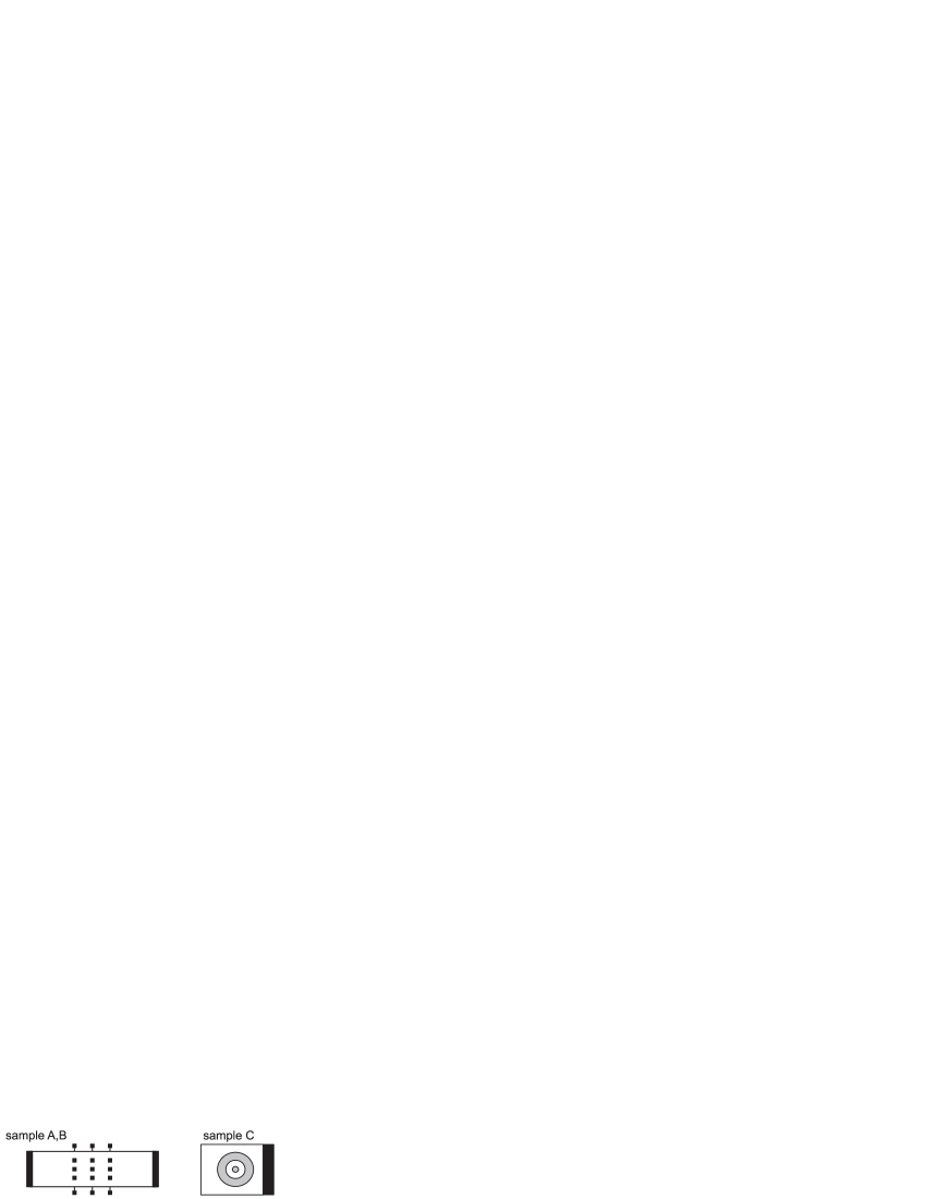
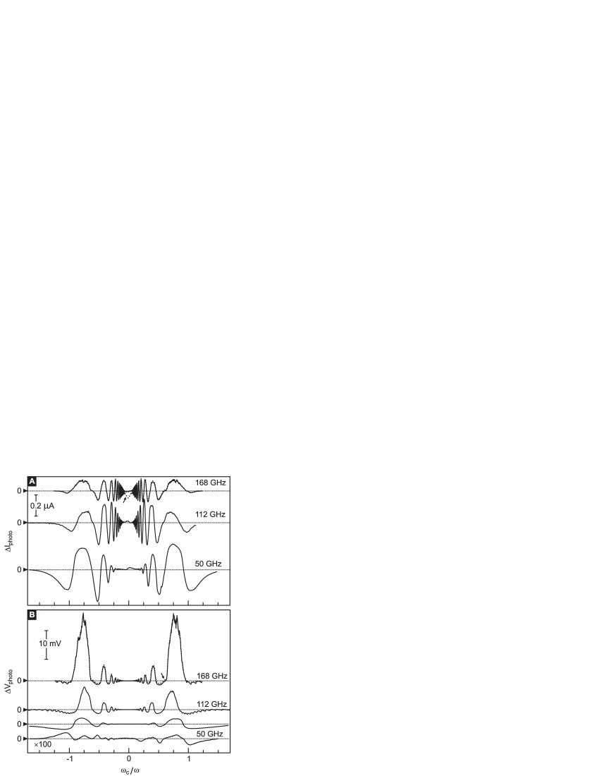
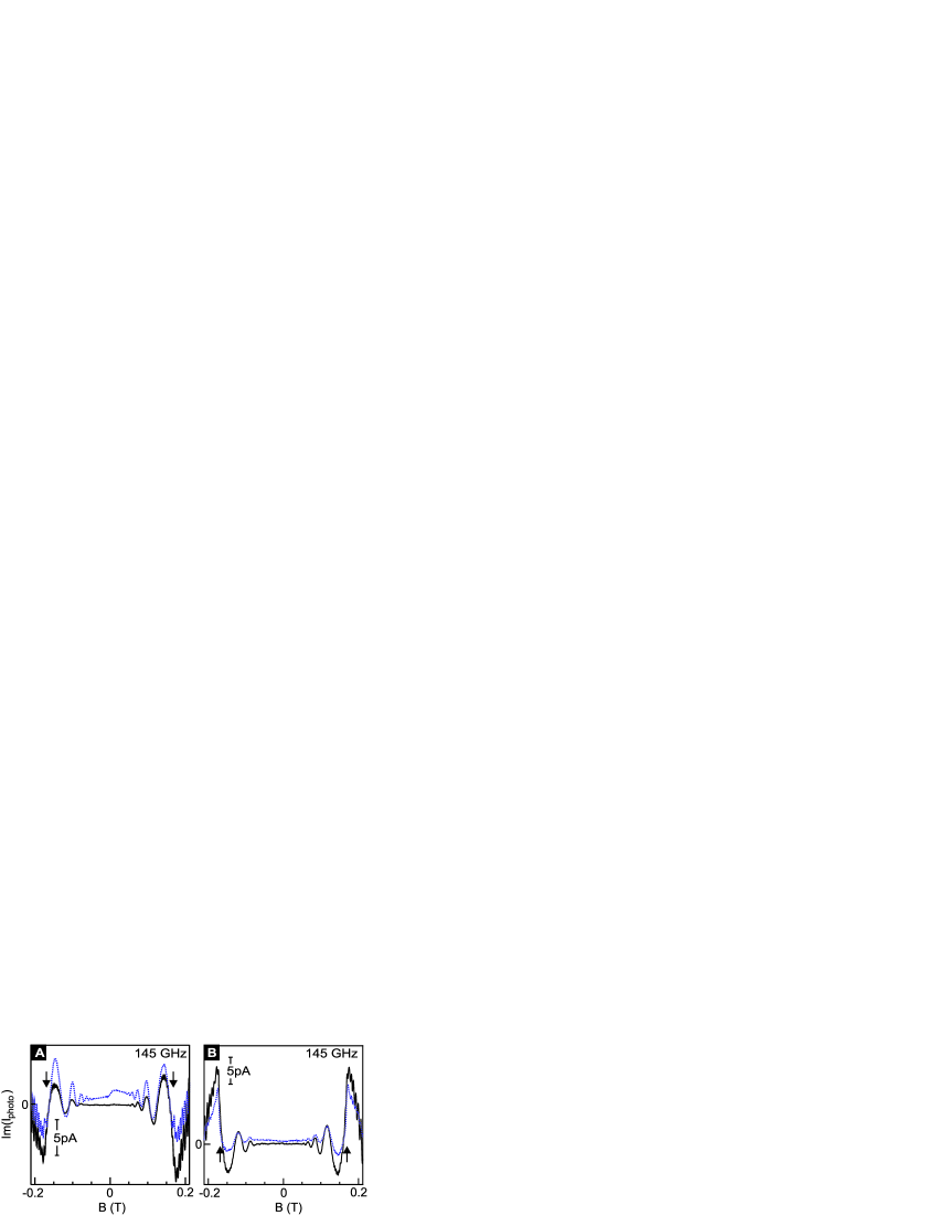
Fig. 2A and B show traces of the DC photo-current and photo-voltage respectively. They were measured between an internal and an external contact. To exclude parasitic signals not induced by the radiation, the plotted data was obtained from a subtraction of signals recorded in the presence and absence of radiation, i.e. and . The parasitic signals and are small as seen from a comparison of the differential signals and with and . The latter have been included as dashed lines for 168 GHz radiation (they are marked by a small arrow). The main parasitic effect appears in the photocurrent near . It originates from the current amplifier when connected to a current source with small impedance (here the sample at small ). The control ac lock-in experiment described previously yields results (not shown) which are in quantitative agreement with those presented in Fig. 2. The photo-voltage measured between any pair of external probes along the perimeter is about two orders of magnitude smaller and quite asymmetric with respect to the -field orientation. An example for 50 GHz is shown at the bottom of Fig. 2B. Internal contacts seem superior in detecting the influence of microwaves. Note the very different shape of the photo-current and the photo-voltage signals. The photo-current oscillations are nearly symmetric with respect to zero and exhibit a non-monotonic dependence of the oscillation amplitude on the -field at high microwave frequencies. The zeroes in and practically coincide for signals measured from all 9 internal contacts. The oscillation amplitude varies by no more than a factor of 1.5 for the photo-voltage and a factor of 2 for the photo-current when comparing signals from different internal contacts. The photo-voltage was also measured between an internal and an external contact while other internal contacts were short circuited to the external probe. The photo-voltage amplitude dropped approximately by a factor of 2 when the nearest neighbor internal contact was short circuited. This contact is at a distance of from the internal contact used in the measurement. The photo-voltage is only weakly or not affected if other internal contacts at a distance of or more are short circuited to the external contact. The photo-current measured when simultaneously connecting two internal contacts to the current amplifier was close to the sum of currents produced by the individual contacts. These observations suggest that the photo-signals arise in the vicinity of each internal contact.
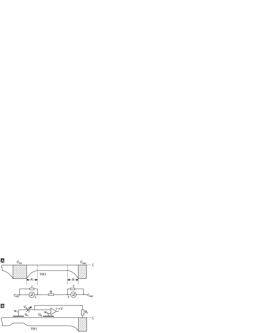
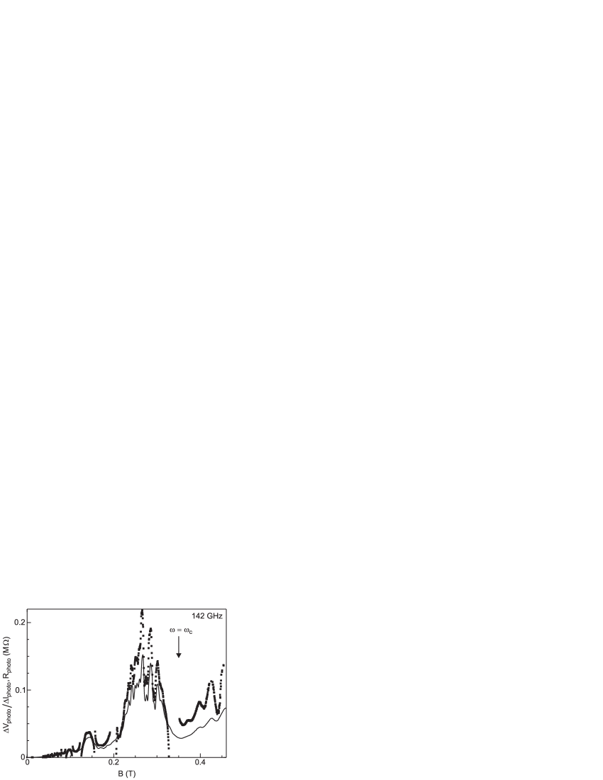
Although both the SAD and NEDF mechanisms provide qualitatively similar results for the photo-current Dorozhkin_tocome and are capable of accounting for our experimental findings, below we will use the easier to visualize SAD picture to explain the experimental data. This picture has also been instrumental in describing the oscillatory behavior of the magnetoresistance Durst ; comment . When Landau levels form and a current is imposed through the sample by applying different electro-chemical potentials at the source and drain contacts, Landau levels are tilted in a direction perpendicular to the current flow due to the Hall electric field. The excitation of an electron to a higher Landau level may then occur even if the microwave photon energy does not match the difference between the Landau level energies (). An appropriate scattering assisted spatial displacement of the electron can simply compensate for the mismatch in order to fulfill energy conservation. If the electron is preferentially displaced down hill and the magneto-resistance increases. For , the electron is promoted against the electric force and the magneto-resistance drops. The photo-current and photo-voltage oscillations can be understood in a similar manner even though no external current to tilt the Landau levels is imposed. The same mechanism is active if built-in electric fields are present. They take over the role of the Hall electric field. The inevitable band bending in the vicinity of contacts as schematically depicted in Fig. 3a is accompanied with built-in electric fields. For a smooth potential variation Landau levels follow this band bending. A spatial displacement of photo-excited electrons allows again to overcome the mismatch between and and a photo-current will flow in a direction which is determined by the built-in electric field and the -field value, i.e. the ratio. The equivalent circuit for this photodiode-like behavior is shown in Fig. 3a. To emphasize that the photo-current can flow in either direction despite the given built-in electric field the current sources have been drawn with a pair of oppositely directed current arrows. For an open current loop, a difference in the quasi-electrochemical potential develops across regions A and A′. It drives compensating currents opposite to the photo-currents to ensure zero net current flow. The shunt resistance for the internal contact and for the external contact introduce this compensating current in the equivalent circuit. For photo-current flow against the built-in electrical field, the generated displacement of electrons effectively enhances this electrical field and hence this field is “anti-screened”. This may lead to an instability and a domain pattern may develop as discussed in Andreev ; Halperin1 . For photo-current flow along the electric field the field is suppressed, i.e. screened, instead. We assume for simplicity that far away from the contacts there are no built-in electric fields, so that this area may in the circuit simply be lumped into a resistor . A pivotal distinction between internal and external contacts is their shunt resistance value. In general . Since an internal contact is entirely surrounded by the 2DES, the shunt resistance is Corbino like and proportional to . Near an external contact however, the shunt resistance is proportional to , which under the experimental conditions is much smaller than . This explains why the role of external contacts is only minor and why a net photo-current is observed in a closed circuit formed between external and internal contacts. It follows from the equivalent circuit that the photo-current and the photo-voltage measured between contacts and are equal to and , respectively. Hence, they are proportional: . The proportionality coefficient is just the two-point resistance between both contacts. This resistance can also be measured independently. It is displayed in Fig. 4 together with . The agreement provides additional support for the proposed scenario. It also explains the shape difference between the photo-voltage and photo-current signals. If it is accepted that band bending at the internal contact occurs as in Fig. 3a and is dominant, also the sign of the photo-current is in accordance with the above explanation. The photo-current will flow within the sample from the internal to the external contact for magnetic fields above the B-field of zero photo-response () and in the opposite direction for fields below the location of zero photo-response (). We note that a vanishing photo-response is predicted by all theories at exactly , but in the reported magnetoresistance data, the oscillation nodes appear at slightly lower -fields than expected for the reported GaAs electron effective mass of (for more details see Refs. Mani2 ; Zudov4 ). This discrepancy with theory remains unexplained, although it could be eliminated when assuming a smaller effective mass Zudov4 . A similar observation holds for the photo-effects discussed here.
To further corroborate that built-in electric fields are responsible for the photo-current and photo-voltage oscillations we have carried out additional experiments in which the potential profile within the sample can be tuned with the help of gates. The geometry is shown in the right panel of Fig. 1 and in Fig. 3b. A voltage is applied either to gate , while gate and the ohmic contact are grounded or vice versa. The gates are also used to detect the capacitive alternating photo-current generated by a train of microwave pulses at a frequency of 1 kHz and with a duty cycle of . The experiment in essence monitors the redistribution of charges underneath the gates brought about by the radiation. The large resistor in the measurement circuit of Fig. 3b suppresses photo-current flow through the alloyed contact, so that the dominant current in the sample flows between gated areas. Experimental results for different values of are plotted in Fig. 5 and reveal oscillations similar to those shown in Fig. 2. At fields larger than 0.2 T, the signals are strongly affected by the Shubnikov-de Haas effect and hence we focus on lower fields. The oscillations appear already at and are either enhanced or suppressed by the application of a non-zero gate voltage. In Fig. 5A signals are compared for (black curve) and (blue dotted curve). At the oscillations are enhanced significantly. Positive values of in the same configuration would cause leakage through the gate. Instead we may interchange the role of gate and (i.e. connect wire to and wire to gate in Fig. 3b). The oscillations in the capacitive photo-current are now suppressed when drops from 0 (black curve) to (blue dotted line). Note that for this modified configuration the photo-current has the opposite sign, i.e. maxima turned into minima and vice versa. The influence of the negative gate voltage agrees with the phase of the oscillations at . For the data imply that there is a net band bending between the gated areas which produces a photocurrent in the sample flowing from the -area to the -area when and from the -area to the -area when . The application of a negative voltage to gate should then enhance this band bending and the amplitude of the microwave induced oscillations should change as observed in Fig. 5A. Conversely, a negative gate voltage applied to gate G2 diminishes the net band bending and the oscillation amplitude should drop. This is indeed born out in the experiment of Fig. 5B. These results show that the existence of alloyed contacts is not crucial for the observation of the oscillating photo-signals.
In summary, incident microwave radiation induces photo-current and photo-voltage oscillations as a function of the applied -field. By modifying the local electrostatic potential the oscillation amplitude can be controlled. The oscillations around zero current or voltage can be understood at a qualitative level assuming built-in electric fields and the scattering assisted displacement of photo-excited electrons Ryzhii1 . A quantitative study based on the SAD mechanism or the NEDF mechanism, which can also qualitatively explain the photo-signals, is called for. The different signs of the photo-signals reflect either the suppression or enhancement of the built-in electric fields.
The authors acknowledge financial support from INTAS, RFBR (SID and IVP) the GIF, the BMBF and the DFG.
References
- (1) R. G. Mani et al., Nature 420, 646 (2002).
- (2) M. A. Zudov et al., Phys. Rev. Lett. 90, 046807 (2003).
- (3) M. A. Zudov et al., Phys. Rev. B 64, 201311(R) (2001).
- (4) P. D. Ye et al., Appl. Phys. Lett. 79, 2193 (2001).
- (5) C. L. Yang et al., Phys.Rev.Lett., 91, 096803 (2003).
- (6) S. I. Dorozhkin, JETP Lett. 77, 577 (2003).
- (7) I. A. Dmitriev et al., Phys. Rev. B 71, 115316 (2005).
- (8) V. I. Ryzhii, Phizika Tverdogo Tela 11, 2577 (1969) (Sov. Phys. - Solid State 11, 2078-2080 (1970)).
- (9) A. C. Durst et al., Phys. Rev. Lett. 91, 086803 (2003).
- (10) R. L. Willett, L. N. Pfeiffer, K. W. West, Phys. Rev. Lett., 93, 026804 (2004).
- (11) A. A. Bykov, JETP Lett. 87, 233 (2008).
- (12) M. G. Vavilov et al., Phys. Rev. B 70, 161306(R) (2004).
- (13) S. I. Dorozhkin, I. A. Dmitriev, and A. D. Mirlin, unpublished.
- (14) Note that the mechanism considered in Ref. Ryzhii1 is only one possible contribution to the photo-response in the magnetoresistance. The dominant contribution is the non-equilibrium occupation of electronic states Dmitriev1 ; Dorozhkin2 .
- (15) I. V. Pechenezhskii, S. I. Dorozhkin, and I. A. Dmitriev, JETP Lett. 85, 86 (2007); S. I. Dorozhkin et al., JETP Lett. 86, 543 (2007).
- (16) A. V. Andreev, I. L. Aleiner, and A. J. Millis, Phys. Rev. Lett. 91, 056803 (2003).
- (17) A. Auerbach et al., Phys. Rev. Lett. 94, 196801 (2005).
- (18) M. A. Zudov, Phys. Rev. B 69, 041304(R) (2004).
- (19) R. G. Mani et al., Phys. Rev. Lett., 92, 146801 (2004).