Andreev reflection in graphene nanoribbons
Abstract
We study Andreev reflection in graphene nanoribbon/superconductor hybrid junctions. By using a tight-binding approach and the scattering formalism we show that finite-size effects lead to notable differences with respect to the bulk graphene case. At subgap voltages, conservation of pseudoparity, a quantum number characterizing the ribbon states, yields either a suppression of Andreev reflection when the ribbon has an even number of sites in the transverse direction or perfect Andreev reflection when the ribbon has an odd number of sites. In the former case the suppression of Andreev reflection induces an insulating behavior even when the junction is biased; electron conduction can however be restored by applying a gate voltage.
pacs:
74.45.+c, 73.23.-b, 72.10-dI Introduction
Graphene, a flat monolayer of Carbon atoms arranged in a two-dimensional (2D) honeycomb lattice, is a newly realized 2D electron system reviews which has attracted a great deal of interest because of the novel physics which it exhibits and because of its potential as a new material for electronic technology. One of the fascinating aspects of this system is that in most cases its potentialities for device applications are intimately related with fundamental aspects of quantum mechanics. Many of the transport properties of graphene which are at the heart of the design of new functional nanostructures originate from conservation laws of certain quantum numbers. For example, the fact that electrostatic barriers in graphene are perfectly transparent to electrons scattering with angles close to normal incidence (Klein-paradox) is explained klein in terms of conservation of pseudospin (the sublattice degree-of-freedom necessary to describe graphene’s non-Bravais honeycomb lattice reviews ).
Early investigations on transport properties of graphene have analyzed current and noise in the presence of normal leads. Recent studies beenakker_prl_2006 ; Ludwig ; Linder ; Levy-Yeyati ; Cayssol ; Prada ; gen_ref have pointed out that novel interesting phenomena arise when graphene is interfaced to a superconductor (SC). In the seminal papers by Beenakker and coworkers beenakker_prl_2006 it has been shown that the peculiar band structure of graphene gives rise to the appearance of specular Andreev reflection (AR) andreev_JEPT_1964 , a novel type of AR that is absent in ordinary metal/SC interfaces. These studies paved the way to experimental investigations of the proximity effect Bouchiat ; Miao and of supercurrent flow Heersche ; Du in graphene. On the theoretical side the results of Ref. beenakker_prl_2006, have been extended in a number of ways, e.g. to graphene bilayers Ludwig and to the case of interfaces with -wave SCs Linder , whereas further studies have focused on the subgap structure of SC-graphene-SC junctions Levy-Yeyati , on crossed AR Cayssol , and on magneto-transport Prada .
Most of the theoretical analysis carried out so far describe the graphene sheet as an infinite (or semi-infinite) 2D plane, and identify two energy scales relevant for transport, namely the superconducting gap and the potential difference between the normal side and the superconducting side, which allows, for instance, to switch from the regime of ordinary AR to the one of specular AR. In graphene ribbons GNR_exp , however, the finite size of the sample yields an additional energy scale , characterizing the mean energy spacing between the ribbon bands. Since the typical ribbon size varies from up to GNR_exp , can range from down to , and it is thus larger than (or of the same order of) the typical superconducting gap . As a consequence, is expected to play an important role in electron transport and AR in graphene.
In the present work we address this problem by analyzing electronic transport through a hybrid junction between a Graphene NanoRibbon (GNR) GNR_theory ; Brey-Fertig ; onipko and a SC, as sketched in Fig. 1.
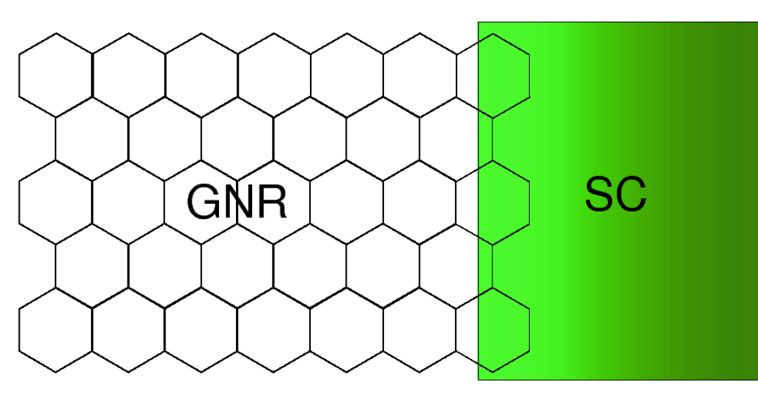
We consider the case of a GNR with zigzag edges, which has been shown to represent fairly well the behavior of an arbitrarily shaped edge akhmerov_beenakker .
Novel effects emerge due to the finite size of the GNR. We find that AR is strongly affected by the conservation of pseudoparity, a quantum number characterizing the GNR eigenstates, which depends on whether the number of sites along the transverse direction is even or odd. In particular, while in GNRs with odd the AR coefficient is unity for subgap voltages, in GNRs with an even AR is totally suppressed. In the latter case AR can be restored to a finite value by applying a gate voltage. Even-odd effects with the same physical origin have been also found in normal transport through graphene p-n junctions (valley-valve effect) wakabayashi_ijmpB_2002 ; akhmerov_prb_2008 ; grosso_prb_2008 .
The contents of the paper are briefly described as follows. In Sect. II we introduce the tight-binding Hamiltonian that we use to model the GNR and provide analytical expressions for the GNR eigenfunctions at arbitrary energy, briefly discussing how transport properties of the hybrid GNR/SC junction are calculated. In Sect. III we report and discuss our results. Finally, in Sect. IV we summarize our main conclusions.
II Model Hamiltonian, GNR eigenfunctions, and transport properties
We model the hybrid GNR/SC system by means of a tight-binding approach. In order to interpret the results presented below, we start by describing the eigenstates in the “normal” side of the junction (the GNR side). The GNR Hamiltonian is a matrix with elements , where eV is the hopping energy between nearest-neighbor sites on the honeycomb lattice, and accounts for a constant electrostatic energy, which can be controlled by a gate voltage.
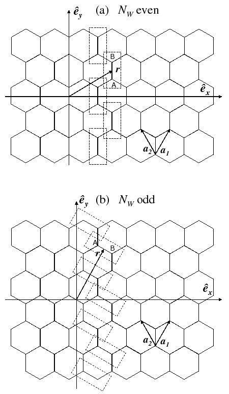
Denoting by and the honeycomb-lattice basis, each unit cell is labeled by a vector , with and integers. The origin is located at the geometrical center of the GNR and is the number of sites in the transverse direction . A suitable shape of the cells turns out to depend on whether is even or odd, as depicted in Fig. 2. It can be shown that the (unnormalized) eigenfunctions of a zigzag GNR at a cell are given by footnote_solution
| (1) |
where is the coordinate of the site of the cell along the longitudinal direction , is the wavefunction along the transverse direction at , and is a spin label. Explicitly, if is even, whereas if is odd ( Å is the Carbon-Carbon distance). Furthermore
| (2) |
where approximately coincides with the width of the GNR, with denoting the integer part of . The eigenvalues related to (1) read
| (3) |
where
| (4) |
and is the solution of (see also Ref. onipko, ). The quantity () is the component of the momentum along (). Importantly, beside the momentum, the eigenstates defined in Eqs. (1)-(2) exhibit an additional quantum number , which determines whether the transverse cell wavefunction is even or odd with respect to the longitudinal axis of the GNR. One can therefore term as pseudoparity. Note that, in contrast to what happens in bulk graphene, the states (1)-(2) are not eigenstates of the pseudospin-projection operator for any unit vector .
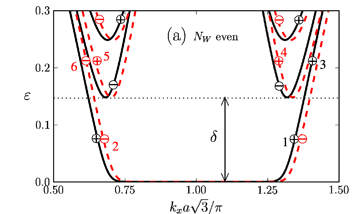
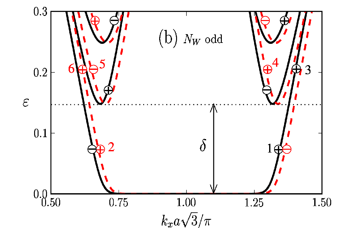
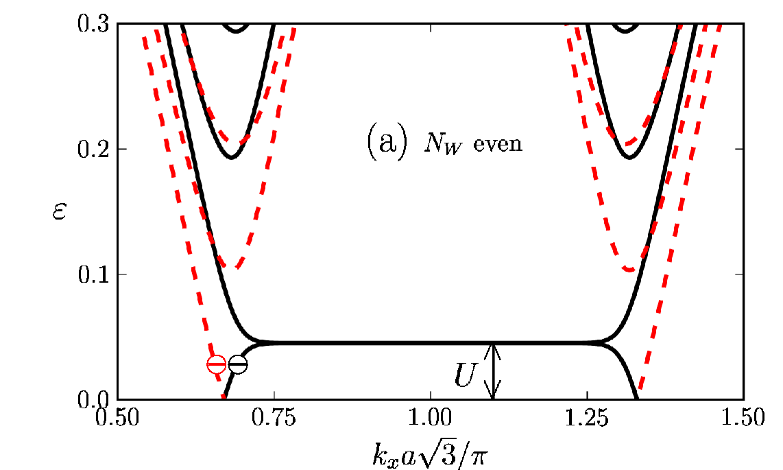
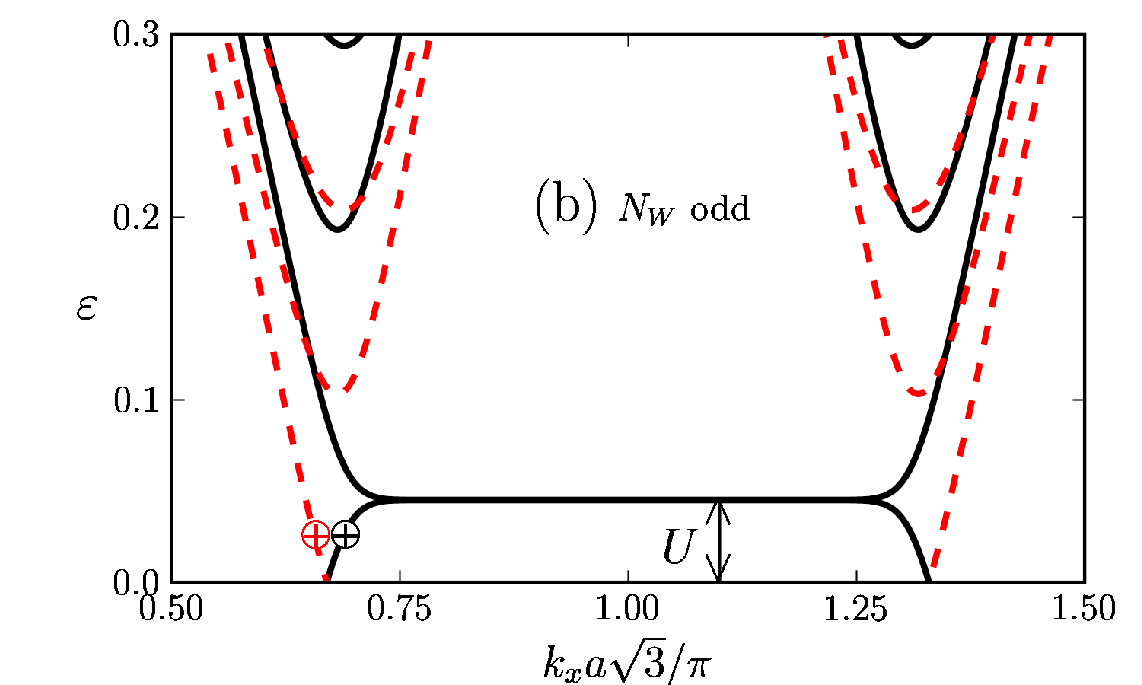
The eigenvalues as functions of describe the band structure of the zigzag GNR, where two bands exhibit dispersionless zero modes and the other ones are somewhat reminiscent of the bulk-graphene Dirac cones reviews , as illustrated in Fig. 3 for the case . Energies are measured with respect to the Fermi level, and solid (dashed) lines refer to particles (holes) bands, which are degenerate for this particular case. The value of the pseudoparity , shown inside the circles, alternates from a particle band to the next one, and takes opposite values in particle and hole bands. Importantly, in the range , the pseudoparity of a GNR with even is opposite to the one for the case with odd .
The energy separation between the first band and the zero-mode energy (Dirac level) is given by for even or for odd Beenakker_bands . A finite shifts the energy of the Dirac level away from the Fermi level, as shown in Fig. 4, breaking particle-hole degeneracy.
The presence of the superconducting electrode is accounted for by the Bogoliubov-de Gennes Hamiltonian degennes
| (5) |
where is the particle Hamiltonian, and is the Fermi level of the GNR/SC junction at equilibrium. The SC (-wave) order parameter, which couples particles and holes, is described by a matrix with entries . Here is taken to vary smoothly across the junction, between its maximum value in the bulk of the SC and zero in the bulk of the GNR footnote_steplike .
Within the scattering approach Datta the zero-temperature differential conductance is given by smatrix
| (6) |
where is the bias voltage applied across the junction. In Eq. (6) the prefactor is due to spin and valley degeneracies, whereas , and are the number of transverse propagating modes (open channels) available at energy measured from the Fermi level , the normal reflection coefficient, and the AR coefficient, respectively. Below the gap () only AR processes can contribute to the conductance, since the unitarity of the scattering matrix implies that in this range.
III Results and discussion
We present our numerical results focusing on the physically realistic regime . We first discuss the case where the Fermi level lies at the Dirac level () and then the case with a finite gate voltage .
III.1 Zero gate voltage
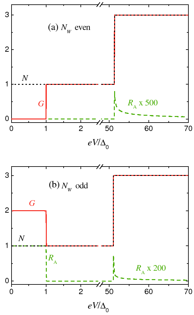
In Fig. 5(a) we plot , , and , as functions of the bias voltage applied across the junction, for a GNR with even , and in Fig. 5(b) we plot the same quantities for a GNR with odd . In the subgap regime a striking dependence on the number of sites arises. While for even the AR coefficient vanishes, the opposite occurs for odd , where is unity. Because for electron transport is possible only by virtue of AR processes, the conductance also vanishes in this voltage range for even . In contrast, for odd , takes its maximum value in the same voltage range. In the regime , where quasi-particle transmission becomes possible, drops abruptly to zero also for odd . This is due to the fact that the transmission processes, which are characterized by a small momentum transfer (intra-valley), largely dominate over AR processes, which instead involve large momentum transfer (inter-valley). We thus find a finite conductance with a value equal to the number of open channels (in units of ). Finally, for , is finite but quite small in both cases (for clarity has been multiplied by an enhancement factor), since voltages in this range are well above the superconducting gap.
These features ( for if is even and for if is odd) can be understood in terms of a pseudoparity superselection rule for the scattering states of the GNR. Let us consider a right-moving incoming electron (labeled by “1” in Fig. 2) with an energy lying between and the bottom of the second band. The only hole state available for an AR process is the one labeled by “2”, which is characterized by a pseudoparity that is (i) opposite to the one of the incoming electron for even and (ii) equal to the one of the incoming electron for odd .
A superconducting parameter that is constant along the transverse direction cannot couple states with opposite pseudoparity (i.e. the pseudoparity of an electron impinging onto the SC interface cannot be flipped). Thus for even the AR process is forbidden and vanishes, whereas for odd this process is allowed and is finite. Notice that in the latter case normal reflection is forbidden by pseudoparity conservation, yielding in the subgap regime. For normal transmission is the dominating process, so that is strongly suppressed for both even and odd . A finite AR is restored for . Indeed in this case intra-valley scattering into hole states with the appropriate pseudoparity [“4” in Figs. 3(a) and Fig. 3(b)] is available. This superselection rule is the ribbon counterpart of the bulk Klein-paradox selection rules based on pseudospin klein and also explains the valley-valve effect in p-n junctions in GNRs wakabayashi_ijmpB_2002 ; akhmerov_prb_2008 ; grosso_prb_2008 .
III.2 Finite gate voltage
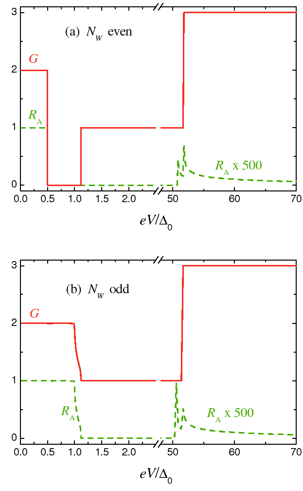
Let us now consider the case (and ). In Fig. 6 we plot our results for , , and .
A comparison between Fig. 5(a) and Fig. 6(a) shows that the application of a gate voltage has dramatic consequences on electron conduction in GNRs with even . This is evident from Fig. 4(a). AR processes are allowed by pseudoparity conservation in the bias range , while they are forbidden for . This fact is reflected in the results shown in Fig. 6(a), where the differential conductance is finite (and equal to ) for and vanishes in the range footnote_sqrt . For subgap voltages electron conduction can be switched on and off by the application of a gate voltage. The junction between an even- GNR and a SC exhibits the operational behavior of an electron transistor based on the pseudoparity conservation law.
In contrast, for odd the application of a gate voltage is expected to have no major qualitative impact on the transport properties of a junction between a GNR with odd and a SC. Once again, this expectation can be traced back to the pseudoparity quantum number, as depicted in Fig. 4(b). The data reported in Fig. 6(b) show indeed the same qualitative behavior reported in Fig. 5(b). The only slight modification is that the drop of to zero, in the range , is less abrupt than in Fig. 5(b), due to a slight momentum mismatch in the transmission channel between GNR and S sides, arising when .
IV Conclusions
In summary, we have studied Andreev reflection in graphene nanoribbon/superconductor hybrid junctions.
We have reported analytical expressions for the eigenfunctions of the tight-binding Hamiltonian describing the graphene nanoribbon, which are valid at arbitrary energy and carry explicitly a definite pseudoparity. The superselection rule stemming from this quantum number has two main implications on transport through the hydrid junction. For narrow nanoribbons with an even number of sites in the transverse direction we have found a complete suppression of Andreev reflection in a range of energies that is huge when the Fermi energy lies at the Dirac level. This implies zero conductance at subgap voltages, which can however be restored applying a finite gate potential, opening up potential technological applications of these hybrid junctions as electron transistors as well as nanorefrigerators. In contrast, in the case of narrow nanoribbons with an odd number of sites we have found perfect Andreev reflection at subgap voltages and an abrupt suppression of it at supergap voltages.
The study of non-ideal edges, realistic interfaces, and bulk disorder is beyond the scope of the present work and is postponed to a future publication diego_dopo . The role of electron-electron interactions and/or next nearest-neighbor hopping, which also has not been addressed in the present work, can be qualitatively understood along the following lines. These effects have been shown to lead to the opening of a gap at the Dirac level reviews ; GNR_theory , which is however typically much smaller than . Our conclusions thus remain valid for a large range of energies even when these effects are taken into account.
Acknowledgements.
We gratefully acknowledge Carlo Beenakker and Francisco Guinea for very useful discussions and suggestions. This work has been partly supported by the NANOFRIDGE EU Project and by the CNR-INFM “Seed Projects”.References
- (1) A.K. Geim and K.S. Novoselov, Nature Mater. 6, 183 (2007); A.K. Geim and A.H. MacDonald, Phys. Today 60(8), 35 (2007); A.H. Castro Neto, F. Guinea, N.M.R. Peres, K.S. Novoselov, and A. K. Geim, arXiv:0709.1163v2.
- (2) M.I. Katsnelson, K.S. Novoselov, and A.K. Geim, Nature Phys. 2, 620 (2006).
- (3) C.W.J. Beenakker, Phys. Rev. Lett. 97, 067007 (2006); M. Titov and C.W.J. Beenakker, Phys. Rev. B74, 041401(R) (2006); C.W.J. Beenakker, arXiv:0710.3848v2.
- (4) T. Ludwig, Phys. Rev. B75, 195322 (2007).
- (5) J. Linder and A. Sudbø, Phys. Rev. Lett. 99, 147001 (2007) and Phys. Rev. B77, 064507 (2008).
- (6) J.C. Cuevas and A. Levy Yeyati, Phys. Rev. B74, 180501 (2006).
- (7) J. Cayssol, Phys. Rev. Lett. 100, 147001 (2008).
- (8) E. Prada, P. San-Jose, B. Wunsch, and F. Guinea, Phys. Rev. B75, 113407 (2007).
- (9) See for example S. Bhattacharjee and K. Sengupta, Phys. Rev. Lett. 97, 217001 (2006); A.G. Moghaddam and M. Zareyan, Phys. Rev. B74, 241403(R) (2006); M. Titov, A. Ossipov, and C.W.J. Beenakker, ibid. 75, 045417 (2007); A.R. Akhmerov and C.W.J. Beenakker, ibid. 75, 045426 (2007); A. Ossipov, M. Titov, and C.W. J. Beenakker, ibid. 75, 241401(R) (2007); D. Greenbaum, S. Das, G. Schwiete, and P. G. Silvestrov, ibid. 75, 195437 (2007); M. Maiti and K. Sengupta, ibid. 76, 054513 (2007); J. Gonzalez and E. Perfetto, ibid. 76, 155404 (2007); S. Bhattacharjee, M. Maiti, and K. Sengupta, ibid. 76, 184514 (2007); G. Tkachov, ibid. 76, 235409 (2007); K. Sasaki et al., J. Phys. Soc. Jpn. 76, 033702 (2007); B. Uchoa and A.H. Castro Neto, Phys. Rev. Lett. 98, 146801 (2007); A.R. Akhmerov and C.W.J. Beenakker, ibid. 98, 157003 (2007); C.W.J. Beenakker, A.R. Akhmerov, P. Recher, and J. Tworzydło, Phys. Rev. B77, 075409 (2008); T. Yokoyama, J. Linder, and A. Sudbo, ibid. 77, 132503 (2008); P. Burset, A. Levy Yeyati, and A. Martín-Rodero, ibid. 77, 205425 (2008); J. Linder, T. Yokoyama, D. Huertas-Hernando, and A. Sudbø, Phys. Rev. Lett. 100, 187004 (2008); C. Benjamin and J.K. Pachos, arXiv:0802.3181v1; A.M. Black-Schaffer and S. Doniach, arXiv:0803.3574v1; M. Zareyan, H. Mohammadpour, and A.G. Moghaddam, arXiv:0804.2774v1 and other related works cited in these papers.
- (10) A.F. Andreev, Sov. Phys. JETP 19, 1228 (1964).
- (11) A. Shailos, W. Nativel, A. Kasumov, C. Collet, M. Ferrier, S. Gueron, R. Deblock, and H. Bouchiat, arXiv:cond-mat/0612058v2.
- (12) F. Miao, S. Wijeratne, U. Coskun, Y. Zhang, and C.N. Lau, arXiv:cond-mat/0703052v2.
- (13) H.B. Heersche, P. Jarillo-Herrero, J.B. Oostinga, L.M.K. Vandersypen, and A.F. Morpurgo, Nature 446, 56 (2007).
- (14) X. Du, I. Skachko, and E.Y. Andrei, Phys. Rev. B77, 184507 (2008).
- (15) Z. Chen, Y.-M. Lin, M.J. Rooks, and P. Avouris, Physica E 40, 228 (2007); M.Y. Han, B. Özyilmaz, Y. Zhang, and P. Kim, Phys. Rev. Lett. 98, 206805 (2007); X. Li, X. Wang, L. Zhang, S. Lee, and H. Dai, Science 319, 1229 (2008); X. Wang, Y. Ouyang, X. Li, H. Wang, J. Guo, and H. Dai, Phys. Rev. Lett. 100, 206803 (2008); Y.-M. Lin, V. Perebeinos, Z. Chen, and P. Avouris, arXiv:0805.0035v2.
- (16) See e.g. Y.-W. Son, M.L. Cohen, and S.G. Louie, Phys. Rev. Lett. 97, 216803 (2006); V. Barone, O. Hod, and G.E. Scuseria, Nano Lett. 6, 2748 (2006); L. Yang, C.-H. Park, Y.-W. Son, M.L. Cohen, and S.G. Louie, Phys. Rev. Lett. 99, 186801 (2007).
- (17) L. Brey and H.A. Fertig, Phys. Rev. B75, 125434 (2007).
- (18) L. Malysheva and A. Onipko, Phys. Rev. Lett. 100, 186806 (2008).
- (19) A.R. Akhmerov and C.W. Beenakker, Phys. Rev. B77, 085423 (2008).
- (20) K. Wakabayashi and T. Aoki, Int. J. Mod. Phys. B 16, 4897 (2002).
- (21) A.R. Akhmerov, J.H. Bardarson, A. Rycerz, and C.W.J. Beenakker, Phys. Rev. B77, 205416 (2008).
- (22) A. Cresti, G. Grosso, and G. Pastori Parravicini, Phys. Rev. B77, 233402 (2008).
- (23) For any the equation has real solutions , except in the range where one solution is imaginary and corresponds to the evanescent wave of the zero mode, see M.I. Katsnelson and F. Guinea, arXiv:0804.2348v1; A. Rycerz and C.W.J. Beenakker, arXiv:0709.3397v1; A. Rycerz, arXiv:0710.2859v2.
- (24) A. Rycerz, J. Tworzydlo, and C.W.J. Beenakker, Nature Phys. 547, 172 (2007).
- (25) P.G. de Gennes, Superconductivity of Metals and Alloys (Addison-Wesley, NewYork, 1989).
- (26) Notice that, since graphene honeycomb lattice is bipartite, a simplified model in which is assumed as a step-like function along the direction would effectively imply a rapid variation of also transversally along the two-site cells. Since such situation would not be realistic, we have adopted a smooth variation of , over a length along the direction.
- (27) S. Datta, Electronic Transport in Mesoscopic Systems, (Cambridge Studies in Semiconductor Physics and Microelectronic Engineering, Cambridge, 1995).
- (28) G.E. Blonder, M. Tinkham, and T.M. Klapwijk, Phys. Rev. B25, 4515 (1982); C.J. Lambert, J. Phys. C 3, 6579 (1991); C.J. Lambert and R. Raimondi, ibid. 10, 901 (1998).
- (29) The fact that vanishes in the range can also be understood in terms of pseudoparity conservation.
- (30) D. Rainis et al., in preparation.