Strategies for triple-donor devices fabricated by ion implantation.
Abstract
Triple donor devices have the potential to exhibit adiabatic tunneling via the CTAP (Coherent Tunneling Adiabatic Passage) protocol which is a candidate transport mechanism for scalable quantum computing. We examine theoretically the statistics of dopant placement using counted ion implantation by employing an analytical treatment of CTAP transport properties under hydrogenic assumptions. We determine theoretical device yields for proof of concept devices for different implant energies. In particular, we determine a significant theoretical device yield () for 14 keV phosphorus in silicon with nominal spacing.
1 Introduction
Quantum computer (QC) architectures compatible with conventional silicon processing technologies would seem to be at an advantage over other schemes. This advantage is due to the perceived ability to leverage conventional silicon processing techniques. Of particular interest is the Kane solid-state quantum computer [1] which is based around nuclear spins of phosphorus (31P) donors in an isotopically pure 28Si matrix (Si:P). As all of the controls and couplings are essentially electron spin mediated or effected, an electron spin version version was proposed by Hill et al. [2] that took advantage of global control properties to access the faster electron, rather than nuclear, spin gate times.
The Si:P QC still faces substantial technical challenges before it can become a reality, and effective means of transport such as that proposed by CTAP (Coherent Tunneling Adiabatic Passage) [3] offer significant flexibility in overcoming these challenges. Amongst these challenges are the expected penalty for linear nearest neighbour (LNN) architectures in decreased threshold for fault-tolerant error correction due to extra SWAP operations [4, 5], and with Si:P, valley degeneracy leads to sensitivity of most critical parameters to variations in donor positions at the atomic level [6, 7]. Both these problems can be ameliorated by the use of effective long-range transport which allows the LNN bottleneck to be avoided, and the incorporation of defect-tolerant design methodologies. An architecture based around transport via CTAP was recently proposed [8] and a threshold analysis performed for a bilinear geometry [4]. The use of CTAP transport rails as designed in [8] also avoids a complex classical control issue, namely the prohibitively high gate density of the original Kane scheme [9]. Although the proof-of-concept structures that we discuss here do not provide the advantages of CTAP rails, demonstrating three-dopant devices is a critical step towards eventual scalable structures. The preferred method for fabricating longer CTAP chains is hydrogen resist lithography that allows for near-atomic dopant placement [10]. This bottom-up process has recently had remarkable success in creating nanoscale surface structures [11, 12] for quantum devices. However the demonstration of the CTAP mechanism requires the construction of single dopant arrays deep within a silicon substrate. Currently, the quickest route to the construction of a proof-of-principle device is the top-down method of single ion implantation [13] as it can be adapted to such fabrication with existing technologies. Here we investigate this practical method for engineering a three atom device. We show estimates for the times required for high-fidelity CTAP using hydrogenic approximations to the tunnel matrix elements [14] and ion implanted donor positions calculated using the SRIM [15] package. Analytic solutions to the expected time for CTAP based on the adiabaticity criterion allow some statistics of expected device yields to be made, which are of benefit in guiding experimental investigations. We also discuss some of the limitations of our approximations, and point to some of the challenges in identifying complete adiabatic pathways to realise the CTAP protocol.
2 Coherent Tunneling Adiabatic Passage and Adiabaticity
CTAP is a protocol for the spatial transport of a particle between two-points on a quantum chain. In its simplest case this is a three-site protocol with the central chain being a single site. CTAP is the direct spatial analog of the well-known STIRAP protocol from quantum optics [16]. CTAP is distinguished from STIRAP in that with CTAP, all variations in couplings are effected by direct modulation of the wave-function overlaps by either surface gate control or well-proximity. With STIRAP the tunnel matrix elements are strictly electromagnetic field driven [17]. In addition to the electronic transfer exploited for Si:P systems, CTAP has been proposed in atomic lattices [18], Cooper-Pair boxes [19], quantum-dots [3, 20], Bose-Einstein condensates [21, 22], spin chains [23] and for photonic transport through coupled waveguides [24]. The latter case has also been demonstrated in beautiful experiments by Longhi and co-workers [25, 26] which adds significant impetus to the push to demonstrate CTAP in systems of massive particles.
CTAP is also an example of a growing search for direct analogues of existing quantum optical effects in quantum electronic systems, and as the degree of coherence that can be detected increases one should expect more sophisticated effects to be observed. Other than CTAP, there are also proposals for Autler-Townes measurements [27, 28], and coherent-population trapping-like dark state transport protocols [29, 30]. One attraction of quantum electronics over conventional quantum optics lies in the ability to tailor the Hilbert space by construction, rather than being limited by the structures of atomic systems. This flexibility allows new vistas and extensions to be explored, for example the multiple-recipient adiabatic passage of Refs. [31, 32] and the direct spatial analogue of the tripod atom [33].
To effect the CTAP pathway requires the adiabatic transformation of
one of the eigenstates of the system from a known start state to a
desired final state. In the spatial setting we restrict the control
parameters to the tunnel matrix elements which are controlled by
surface electrodes (gates), analogously to the way in which
electro-magnetic field intensities are varied in STIRAP.
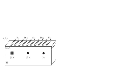
A schematic of the surface structure that we are assuming is shown in
Figure 1LABEL:sub@fig:1a, viewed from the top down. The device structure
shown in Figure 1LABEL:sub@fig:1a is yet to be made and it is the purpose
of this paper to investigate potential fabrication methods based on
presently available technologies. Devices of comparable complexity
have been fabricated using the counted-ion implantation techniques described in
Ref. [13], and we also note the demonstration
of triple dots in GaAs 2DEG structures [34, 35, 36]
and gated carbon nanotubes [37].
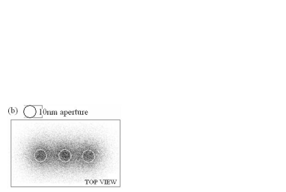
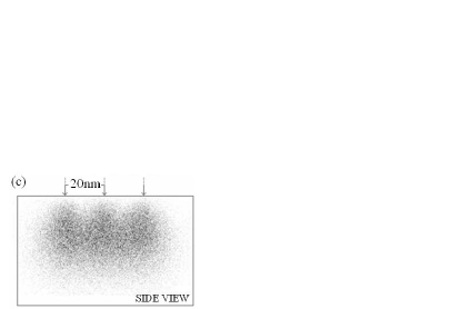
Ideally we would like three donor atoms spaced 20-30 nm apart, 20 nm below the surface. The SRIM data in Figures 1LABEL:sub@fig:1b and 1LABEL:sub@fig:1c shows the probability distribution of 100,000 14 keV P+ ions implanted sucessively through three circular apertures 10 nm in diameter. A 14 keV phosphorous ion will travel around 20 nm into the substrate before stopping but can straggle away from this median position by up to 11 nm as it undergoes collisions with the Si lattice. A less energetic 7 keV ion will penetrate 14 nm below the surface and has 40% less straggle than at 14 keV. The straggle imposes constraints on the accuracy of dopant placement. To quantify the consequence of these fabrication perturbations on the ideal donor positions seen in Figure 1LABEL:sub@fig:1a we have used SRIM simulations with a simplified treatment of three-donor CTAP.
We begin by writing down the Hamiltonian of the three donor one electron problem in the three-state approximation (i.e. where we only keep the lowest state of the electron localised around the donor). In the basis with onsite energies (assuming fully compensated) and tunnel matrix elements and , we also include the possibility of next nearest neighbour tunneling (i.e. from to ) however for the discussion that follows this will be assumed to be zero. The Hamiltonian is
| (1) |
and with , the eigenvalues are
| (2) | |||||
| (3) |
with energies
| (4) | |||||
| (5) |
The CTAP protocol can now be understood quite simply. The idea is to remain in the state , and to vary the tunnel matrix elements so that at time , the system is in the desired initial state, e.g. , and at time the system is in the desired final state, e.g. . Note that although this three mode description for the tunneling is obviously a simplification, it still captures all of the essential physics of the CTAP protocol, a fact confirmed by recent analyses of the CTAP in the triple square well case [38].
To effect CTAP, there is clearly a large amount of flexibility to choose the pulsing scheme for the tunnel matrix elements. In STIRAP protocols, gaussian or gaussian-like pulses are most commonly employed because of the necessity to turn on the excitation (laser pulse) before varying it [16]. However in the solid state, where non-zero tunnel matrix elements arise solely due to donor proximity, this necessity is not required, and so we advocate the use of the pulses that vary between their extrema at and . Such pulses are explicitly stated below and illustrated in Figure 2. In Refs. [22, 32, 39] error function pulses were employed which have some advantages in terms of smoothness of evolution and in nonlinear systems avoid certain complications due to eigenstate degeneracy at the ends of the protocol. For simplicity, here we choose sinusoids with the sole purpose of making the analytical results clearer.
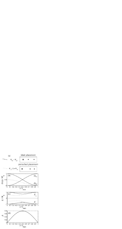
To determine whether the system remains in the target state, we invoke the adiabaticity criterion, and due to symmetry we define (without loss of generality) the adiabaticity parameter to be between and . The adiabaticity parameter is
| (6) |
and for adiabatic evolution we require . One should be mindful of the fact that the adiabaticity does not translate to a direct measure of fidelity, it is rather a measure for when the assumption of adiabatic evolution is justified. Choosing as the form for the (gate controlled) tunnel matrix elements
| (7) | |||||
| (8) |
gives
| (9) |
Of importance here is to note that the adiabaticity is a maximum when irrespective of the relative values of and . This is significant in the design of robust sequences and in affording a quick estimate of the required timescale for CTAP operation. To illustrate the energies, tunnel matrix elements and adiabacity, in Figure 2 we present characteristic plots for the case that and when .
In a realistic experiment, we will want to set the time for CTAP given a certain desired adiabaticity. So it is more important to rearrange (9) to determine the value for that keeps the maximum value of at or below some threshold, which is
| (10) |
where we have dropped the sine term because we are evaluating with respect to the maximum value of .
Equation (10) is particularly useful in gaining insight into the practicalities of CTAP. Although we are not yet in a position to place a lower bound on (in general this must come from a detailed understanding of the higher lying molecular and orbital states, limitations on the pulsing electronics, and accessible surface gate voltage), we can immediately compare our results with realistic upper bounds. The most obvious impediment to very long time scales will be the limits placed by decoherence, which will set a maximum length of time over which the protocol can be conducted [3, 40, 41].
Until now we have neglected the next nearest neighbour tunneling, i.e. . Formally there is no CTAP pathway for non-zero as the Hamiltonian (1) has no null (or dark) state, however we can place a good bound on whether neglecting will be valid by comparing the period for oscillation on the transition directly with the total time for CTAP. We introduce and assert that if then we may ignore the effect of in our analysis. This criterion is helpful for proof of concept devices, but may not suffice for full QC applications where more rigorous error control is required [8].
3 Implications for ion implanted devices
We have treated the Hamiltonian in an ideal case, without regard to the physical nature of our system. If we now turn specifically to phosphorous dopants in silicon, with realistic gate controls, then issues of the suppression of tunnel matrix elements via barrier control, cross-talk between gates [42] and microscopic details of the dopant species become paramount [6]. All such features must be taken into consideration to determine the adiabatic pathway, which is a highly non-trivial task which we do not attempt here. Instead we have focussed on hydrogenic approximations which allow us to gain rapid insight into a variety of implant conditions; we leave the solution of the control problem to future work, assuming (as in Refs. [3, 8]) that the gate controls are able to completely suppress the tunnel matrix element from the maximum (no-field) level to zero.
To determine the bare (unperturbed) tunnel matrix elements, we use the hydrogenic approximation of Openov [14], an approach used ostensibly in the study of singly ionized double-donor structures [43]. These results are applicable to donor separations predominantly along the [100] direction in silicon where the valley degeneracy has less effect [6, 44]. To be explicit, we use
| (11) |
is the effective Hartree, and is the interdonor separation between donor and . With these constraints we can immediately write down and as
| (12) | |||||
| (13) | |||||
| (14) |
A rigorous calculation of and would involve full band structure considerations, but these formulae give an extremely efficient mechanism for determining these important parameters with relatively minimal computational cost, as is required to process the large number of dopant positions that can be obtained using SRIM calculations.
To explore the range of expected yields, we performed SRIM simulations for 14 keV and 7 keV phosphorus. Single 14 keV phosphorous ions are routinely detected entering a silicon substrate [13] and reach a nominal depth of 20 nm below the substrate surface. The lateral straggle of an implanted ion limits the precision of dopant placement and hence the control of donor seperation required to engineer a suitable proof of concept device. Therefore 7 keV was also chosen for the greater placement accuracy it allows and as a guide to future developement of the detection system. A typical oxide thickness of 5 nm was used in the 14 keV strategy while in the low energy strategy we assumed an oxide thickness of an optimal 1.2 nm. The on-chip detection of [13] guarantees that precisely three ions will be implanted, however it does not ensure that there will be one ion per aperture. To ensure this capability a ‘step-and-repeat’ strategy based on existing technologies is currently being integrated with the detection system. A similar approach is being followed by Schenkel et al. [45, 46] and also by Meijer et al. [47] for the creation of nitrogen-vacancy colour centres in diamond.
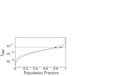
The results of performing SRIM simulations for each implant strategy are shown in Figure 3. In addition to the raw straggle data obtained from SRIM, we have convolved the distributions with apertures 10 nm in diameter, separated linearly by . For each implant triple, we have then calculated and , although as is found to be substantially less than one for over of the triples we have not shown those results here. Figure 3 then shows the cumulative distribution function for the at an adiabaticity of , which may immediately be interpreted as a measure of yield. Upper limits on are given by the decoherence limit. As a rule of thumb, we wish to be at least an order of magnitude faster than decoherence for a significant proof-of-concept signal [3]. To aid comparisons, Figure 3 shows a horizontal line corresponding to 1 ns, which is an order of magnitude less than a realistic expected decoherence time (10 ns). From this we can read off the population of triples which satisfy this criterion for each implant strategy. One should be mindful, however, that the expected device yield even without fabrication errors will be less than this, due to the fraction of donors that are too close (i.e. have too high tunnel matrix elements) to be properly controlled, or to have their tunnel matrix elements adequately suppressed. This bound will be determined in large part by the breakdown of the oxide barrier and is not addressed here.
From the results in Figure 3 we can make some initial estimates of the prospects for ion implantation strategies, and in particular we find that within the limits of our models, we can afford some optimism about the ion implantation as a strategy for proving the concept of CTAP. The expected theoretical yield for the standard 14 keV strategy is predicted to be around , and for the low energy 7 keV strategy it is expected to be closer to .
4 Conclusions
We have performed analysis of implanted donor triples using SRIM to provide guidance to experimental efforts to realise the CTAP (Coherent Tunneling Adiabatic Passage) protocol. Our results suggest theoretical device yields around within the hydrogenic approximation and not including device fabrication errors. To process the large amounts of data generated by SRIM, we developed new analytical results for the required time for high-fidelity CTAP, and applied these metrics to various implantation strategies and species. Our methods are unable to address all of the requirements for CTAP, which include the need to identify the particular adiabatic pathway for a given microscopic location of donors, nor do we go beyond the hydrogenic approximation. More accurate modelling is required, (e.g. NEMO3D [48, 49]) to theoretically describe a given system, but this is far too numerically intensive to explore the very large number of configurations explored here. On the basis of our results, we predict that ion implantation is a sensible strategy to exploit for proof-of-concept CTAP devices, although the overall scaling to the longer CTAP chains required for scalable QC [8] is expected to be far less favorable and hydrogen resist lithography methods for producing such CTAP chains is the preferred method [10].
References
- [1] B. E. Kane, Nature (London) 393, 133 (1998).
- [2] C. D. Hill, L. C. L. Hollenberg, A. G. Fowler, C. J. Wellard, A. D. Greentree, and H.-S. Goan, Phys. Rev. B 72, 045350 (2005).
- [3] A. D. Greentree, J. H. Cole, A. R. Hamilton, and L. C. L. Hollenberg, Phys. Rev. B 70, 235317 (2004).
- [4] A. M. Stephens, A. G. Fowler, and L. C. L. Hollenberg, Quant. Inf. Comp. 8, 330 (2008).
- [5] T. Szkopek, P. O. Boykin, H. Fan, V. P. Roychowdhury, E. Yablonovitch, G. Simms, M. Gyure, and B. Fong, IEEE Transactions on Nanotechnology, 5(1), 42-49, (2006).
- [6] B. Koiller, X. Hu, and S. Das Sarma, Phys. Rev. Lett. 88, 027903 (2002).
- [7] C. J. Wellard and L. C. Hollenberg, Phys. Rev. B 72, 085202 (2005).
- [8] L. C. L. Hollenberg, A. D. Greentree, A. G. Fowler, and C. J. Wellard, Physical Review B 74, 045311 (2006).
- [9] M. Oskin, F. T. Chong, I. Chuang, and J. Kubiatowicz, in Building Quantum Wires: The Long and the Short of It, Proceedings of the 30th Annual International Symposium on Computer Architecture (ISCA), San Diego, June 2003.
- [10] S. R. Schofield, N. J. Curson, M. Y. Simmons, F. J. Rueß, T. Hallan, L. Oberbeck, and R. G. Clark, Phys. Rev. Lett. 91(3), 136104 (2003).
- [11] F. J. Rueß, K. E. J. Goh, M. J. Butcher, T. J. Reusch, L. Oberbeck, B. Weber, A. R. Hamilton, and M. Y. Simmons, Nanotechnology, 18, 044023 (2007).
- [12] F.J. Rueß, W. Pok, T.C.G. Reusch, M.J. Butcher, K.E.J. Goh, G. Scappucci, A.R. Hamilton, and M.Y. Simmons, Small, 3(4), 563-567 (2007).
- [13] D. N. Jamieson et al. Appl. Phys. Lett. 86, 202101 (2005).
- [14] L. A. Openov, Phys. Rev. B 70, 233313 (2004).
- [15] J. F. Ziegler, Nucl. Instrum. Meth. B 219-220, 1027-1036 (2004).
- [16] N. V. Vitanov, T. Halfmann, B. W. Shore and K. Bergmann, Annu. Rev. Phys. Chem. 52, 763 (2001).
- [17] Although we note that STIRAP across a spatial degree of freedom has been proposed in, for example: U. Hohenester, F. Troiani, E. Molinari, G. Panzarini, and C. Macchiavello, Appl. Phys. Lett. 77, 1864 (2000); T. Brandes, F. Renzoni, and R. H. Blick, Phys. Rev. B 64, 035319 (2001); E. Pazy, I. D Amico, P. Zanardi, and F. Rossi, ibid. 64, 195320 (2001).
- [18] K. Eckert, M. Lewenstein, R. Corbalán, G. Birkl, W. Ertmer, and J. Mompart, Phys. Rev. A 70, 023606 (2004).
- [19] J. Siewert and T. Brandes, Adv. in Solid State Phys. 44, 181 (2004).
- [20] D. Petrosyan and P. Lambropoulos, Opt. Commun. 264, 419 (2006).
- [21] E.M. Graefe, H.J. Korsh and D. Witthaut, Phys. Rev. A 73, 013617 (2006).
- [22] M. Rab, J.H. Cole, N.G. Parker, A.D. Greentree, L.C.L. Hollenberg, and A.M. Martin, Phys. Rev. A 77, 061602(R) (2008).
- [23] T. Ohshima, A. Ekert, D. K. L. Oi, D. Kaslizowski, and L. C. Kwek eprint arXiv:quant-ph/0702019.
- [24] S. Longhi, J. Phys. B 40, F189 (2007).
- [25] S. Longhi, G. Della Valle, M. Ornigotti, and P. Laporta, Phys. Rev. B 76, 201101(R) (2007).
- [26] G. Della Valle, M. Ornigotti, T. Toney Fernandez, P. Laporta, S. Longhi, A. Coppa and V. Foglietti, Appl. Phys. Lett. 92, 011106 (2008).
- [27] A. D. Greentree, A. R. Hamilton, and F. Green, Phys. Rev. B 70, 041305(R) (2004).
- [28] A. D. Greentree, A. R. Hamilton, L. C. L. Hollenberg, and R. G. Clark, Phys. Rev. B 71, 113310 (2005).
- [29] B. Michaelis, C. Emary, and C. W. J. Beenakker, Europhysics Letters 73, 677 (2006).
- [30] C. Emary, Phys. Rev. B 76, 245319 (2007).
- [31] A. D. Greentree, S. J. Devitt, and L. C. L. Hollenberg, Phys. Rev. A 73, 032319 (2006).
- [32] S. J. Devitt, A. D. Greentree, and L. C. L. Hollenberg, Quantum Information Processing 6(4), 229-242 (2007).
- [33] K. Deasy, T. Busch, Y. Niu, S. Gong, S. Jin and S. Nic Chormaic, eprint arXiv:quant-ph/0611174.
- [34] L. Gaudreau, S. A. Studenikin, A. S. Sachrajda, P. Zawadzki, A. Kam, J. Lapointe, M. Korkusinski, and P. Hawrylak, Phys. Rev. Lett. 97, 036807 (2006).
- [35] D. Schröer, A. D. Greentree, L. Gaudreau, K. Eberl, L. C. L. Hollenberg, J. P. Kotthaus, and S. Ludwig, Phys. Rev. B 76, 075306 (2007).
- [36] M. C. Rogge and R. J. Haug, Phys. Rev. B 77, 193306 (2008).
- [37] K. Grove-Rasmussen, H. I. Jørgensen, T. Hayashi, P. E. Lindelof, and T. Fujisawa, Nano Lett. 8(4), 1055, (2008).
- [38] J. H. Cole, A. D. Greentree, L. C. L. Hollenberg, and S. Das Sarma, Phys. Rev. B 77, 235418 (2008).
- [39] A. D. Greentree, J. H. Cole, A. R. Hamilton, and L. C. L. Hollenberg, Proceedings of SPIE International Society of Optical Engineers 5650, 72-80 (2005).
- [40] P. A. Ivanov, N. V. Vitanov, and K. Bergmann, Phys. Rev. A 70, 063409 (2004).
- [41] I. Kamleitner, J. Cresser, and J. Twamley, Phys. Rev. A 77, 032331 (2008).
- [42] G. Kandasamy, C. J. Wellard, and L. C. L. Hollenberg, Nanotechnology 17, 4572-4580 (2006).
- [43] A. V. Tsukanov, Phys. Rev. B 76, 035328 (2007).
- [44] C. J. Wellard, L. C. L. Hollenberg, and S. das Sarma, Phys. Rev. B 74, 075306 (2006).
- [45] A. Persaud, S. J. Park, J. A. Liddle, T. Schenkel, and J. Bokor, I. W. Rangelow, NanoLetters 5 (6), 1087 (2005).
- [46] T. Schenkel et al. Microelectronic Engineering 83(4-9), 1814-1817 (2006).
- [47] J. Meijer et al. Appl. Phys. A 91, 567 571 (2008)
- [48] G. Klimeck, F. Oyafuso, T.B. Boykin, R.C. Bowen, and P. Allmen, Computer Modeling in Engineering and Science, 3(5), 601-642 (2002).
- [49] R. Rahman et al. in preparation.
- [50] A. V. Tsukanov and L. A. Openov, Semiconductors 38(1), 91-98 (2004). Translated from Fizika i Tekhnika Poluprovodnikov, 38(1), 94-101 (2004).
- [51] C. J. Wellard, L. C. L. Hollenberg, F. Parisoli, L. M. Kettle, H. S. Goan, J. A. L. Mc Intosh, and D. N. Jamieson, Phys. Rev. B 68 195209 (2003).
- [52] F. J. Rueß, L. Oberbeck, M. Y. Simmons, K. E. J. Goh, A. R. Hamilton, T. Hallam, S. R. Schofield, N. J. Curson, and R. G. Clark, NanoLetters, 4(10), 1969-1973 (2004).