Theory of defects in one-dimensional systems: the case of Al in Si nanowires
Abstract
The energetic cost of creating a defect within a host material is given by the formation energy. Here we present a formulation allowing the calculation of formation energies in one-dimensional nanostructures, which overcomes the difficulties involved in defining the chemical potential of the constituent species and the possible passivation of the surface. We also develop a formula for the Madelung correction for general dielectric tensors and computational cell shapes. We apply this formalism to the formation energies of charged Al impurities in silicon nanowires, obtaining concentrations significantly larger than in their bulk counterparts.
pacs:
68.35.Dv,73.20.Hb,61.46.KmThe study of the energetics of the formation of defects is a very well-developed topic in bulk semiconductor physics Pantelides (1978); Fahey et al. (1989); Seebauer and Kratzer (2006); Cardona (2007), but it is considerably less mature in nanostructures. A sensible definition of the chemical potential, the possible presence of passivating agents on the surface and a proper treatment of the defect charge state are some of the issues that prevent the extension of the standard theory from being straightforward. The formation energy of a defect Zhang and Northrup (1991) is a quantity of paramount technological importance; it determines the structural configuration and the charge state that a given set of impurities will favor, and it is used in the computation of impurity equilibrium concentrations Zhang and Northrup (1991); Northrup and Zhang (1993); Van de Walle (1994), solubilities Van de Walle et al. (1993); Luo et al. (2004), diffusivities Fahey et al. (1989); Stumpf and Scheffler (1994), dopant compensation mechanisms Laks et al. (1992), etc. In addition, the calculation of the formation energy is required whenever a comparison between configurations with different number of atoms/chemical species is wanted.
In bulk host materials, formation energies are calculated according to the well-established theory due to Zhang and Northrup Zhang and Northrup (1991), where they are formulated in terms of the chemical potentials of the constituent species and the total energy of the system with the impurities. On the other hand, for one-dimensional (1D) semiconductor systems, the nonequivalence of the different constituent atoms in, say, a silicon nanowire (SiNW), in addition to surface passivation issues, render the straightforward application of the Zhang-Northrup formalism troublesome. In particular, the definition of the chemical potential of the atomic species involved is ill-defined. This difficulty is considerably lessened in the study of nanotubes, where each atom is equivalent to the others. This has allowed initial calculations of defect formation energies in C and BN nanotubes Baierle et al. (2001); P Piquini and Fazzio (2005), but analogous calculations for semiconductor nanowires have been missing so far. Additionally, the most stable configuration of a defect in a semiconductor may have a charge state different from zero, depending on the doping condition of the material. In a periodic boundary condition (PBC) formalism, a finite net charge in the simulation cell would give rise to a divergent Coulomb energy because of the interaction with its periodic images. While the correct procedure for the removal of this contribution to the total energy is still a matter of debate, recent reports indicate that the uniform background charge Leslie and Gillan (1985); Makov and Payne (1995) and the local-moment counter charge Schultz (2000) yield similar results Wright and Modine (2006) for bulk materials. However, a treatment for charged defects in one-dimensional systems is lacking so far.
In this Letter we propose a framework for the calculation of formation energies of neutral and charged point defects in 1D systems. As a case study we discuss the formation of Al point defects, which can provide p-doping and can be found as contaminant from Al-catalyzed growth process Wang et al. (2006), thus conveying a considerable technological interest. Specifically, we will deal with substitutional and interstitial defects at different radial positions in and SiNWs of 1.0 and 1.5 nm diameter, identifying whether there is a tendency to surface segregation and their most stable charge state for different doping conditions.
Formation energy in bulk – According to the well-established theory due to Zhang and Northrup Zhang and Northrup (1991), the formation energy of a charged defect in a semiconductor is given by
| (1) |
where () is the total energy of the defective (clean) system, is positive (negative) for atoms added to (removed from) the clean system, is the chemical potential of the reservoir supplying the impurities, is the top of the valence band of the clean host and is the chemical potential for electrons.
Chemical potential – Extending the use of this formalism to one-dimensional nanostructures involves some subtleties related to the definitions of the chemical potential, especially in the case of vacancies, substitutionals and self-interstitials. When a vacancy is formed in bulk, the removed atom is implicitly assumed to be added to the crystal; thus the use of the bulk chemical potential is justified. For a NW, the displaced atom can be added to multiple nonequivalent positions, as opposed to bulk, where all lattice sites are equivalent. This induces an ambiguity with respect to the choice of the chemical potential, but even if somehow a preferred site for the displaced atom were selected, the calculation of its contribution to the total energy would be ill-defined from a computational point of view. In addition, if the NW is passivated, it is not clear how many passivating atoms or fraction thereof should be assigned to the displaced atom. Clearly, any attempt to use Eq. (1) directly will not be able to deal with the possibility that the NWs may be surface passivated.

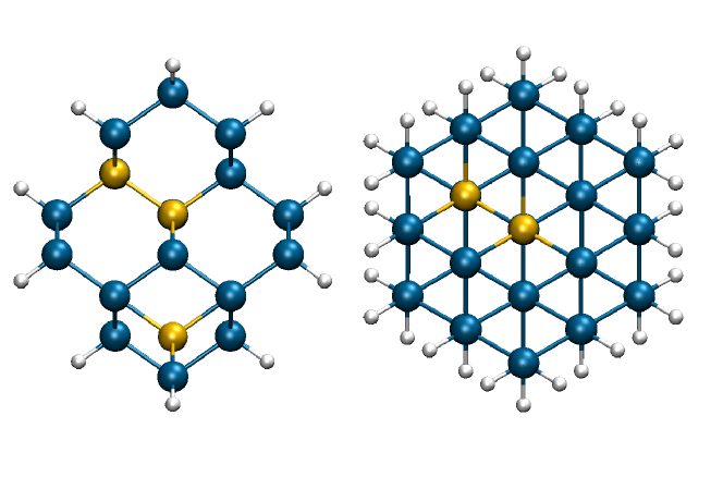
We can circumvent these issues by considering the formation of defects instead of a single defect (see Fig. 1), where is the number of silicon atoms in a NW primitive cell—for the sake of simplicity we will refer to Si atoms, meaning any host material. These displaced atoms are then added at the end of the NW to form an extra primitive cell with the needed passivating agents. We notice that this is equivalent to defining a chemical potential of the wire primitive cell.
With the above or analogous constructions, it is easy to see that a general expression for the formation energy of a given type of defect will be
| (2) |
where is the number of primitive cells used in the clean system calculation, is the energy of the NW clean primitive cell, satisfying , is the number of non-host atoms of species added to the clean system, is their chemical potential, is the number of Si atoms involved in the defect formation (e.g. +1 for a self-interstitial), is the number of passivating atoms in a NW primitive cell (taken to be hydrogens) and is the corresponding chemical potential. All quantities appearing in Eq. (2) are now well defined and easily extracted from a total energy calculation. Note as well that, in the bulk limit, and Eq. (1) is recovered.
Charged defects – The study of charged defects in one-dimensional nanostructures in a PBC formalism must overcome various particularities not present in the bulk case, all arising from the fact that a dielectric tensor will be needed for the correct description of the interaction between the different instances of the charged defect.
The usual procedure for dealing with these effects in bulk materials consists in using a neutralizing jellium background to recover the charge neutrality condition, and then correct a posteriori for the spurious terms arising in the total energy by means of a Madelung correction Ziman (1972) divided by the value of the (isotropic) macroscopic dielectric constant of the host material Makov and Payne (1995).
In the case of a NW, the numeric value of the Madelung constant will depend on the relation between the lattice parameters and the chosen , and thus it cannot be looked up in tables. Starting from the solution to the Poisson equation within a homogeneous, anisotropic medium Fischerauer (1997), and following analogously to the standard procedure Ziman (1972), one can easily obtain the following expression for the Madelung constant in the general case
| (3) |
where the sum over () extends over all vectors of the direct (reciprocal) lattice except for zero, is a suitably chosen convergence factor and is the volume of the primitive cell. This approach, besides dealing with generic dielectric tensors, allows us also to easily tackle non-conventional cell shapes. This is a very common situation in 1D systems, where the axial lattice parameter obeys the periodicity of the crystal structure, while the transverse dimensions are normally much larger. This allows a proper buffer vacuum to avoid spurious interactions with the image neighboring system Mad . Concerning the choice of the dielectric tensor , one would be tempted to use, for example, the modified Penn model Tsu et al. (1997) in order to obtain an approximation to the value of the dielectric constant for directions perpendicular to the growth axis. This would be indeed the correct approach if we were to study the physics of excitons in the NW. However, it must be kept in mind that in the case at hand two images corresponding to different instances of the NW will interact mainly through vacuum if enough buffer space is left. Thus, we will take the dielectric tensor to be , where is the bulk dielectric constant of the constituent material of the NW.
Al defects in and SiNWs – We apply the formalism described above to the study of Al point defects in 1 nm and 1.5 nm SiNWs grown along the and axes. Two reasons make Al impurities a very interesting case study: (i) group-III elements can be efficient p-type dopants for silicon, and the use of Al for doping in nanowires has indeed been proposed Durgun et al. (2007); (ii) Al has proven to be a feasible alternative to Au as a catalyst for the epitaxial growth of SiNWs Wang et al. (2006), having the considerable advantage of not introducing undesired mid-gap states that can act as traps, and requiring lower growth temperatures. We calculate the total energy within density-functional theory, as implemented in the Siesta package Soler et al. (2002), using norm-conserving pseudopotentials, an optimized double- basis set Anglada et al. (2002) and the spin-polarized version of the generalized gradient approximation (GGA) Perdew et al. (1996) for the exchange-correlation energy. The supercell size was chosen to guarantee a separation of 23.7 Å (28.3 Å) between the impurity and its periodic image along the () axis, while the transverse dimensions were held at 50 Å. The atomic positions were relaxed until the forces on all the atoms were lower than 0.02 eV/Å and the axial lattice parameter was optimized for the pristine wire for each growth orientation Vo et al. (2006). If an Al nanoparticle is used to catalyze the growth reaction, the nanoparticle will be the main source of Al contaminants in the SiNW. Therefore, we define the Al chemical potential with respect to an Al particle of approximately the same diameter of the wire.

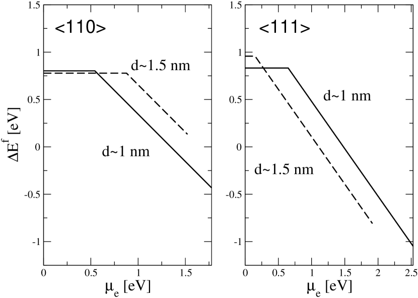
At first we have considered Al substitutional impurities, Al, at two different radial coordinates, and the tetragonal interstitial, Al, in 1 nm and SiNWs (see Fig. 2). As expected, Al is a single acceptor, with substitution at a host lattice site being largely favored over the interstitial position (see Fig. 3). Despite the thin diameter of the wire, the formation energy of the Al is hardly sensitive to the change in the radial coordinate of the lattice site; the only noticeable change is a slight lowering of the occupation level of the wire when the Al substitutes moves outwards (dashed line in Fig. 3). We have not observed any marked tendency to surface segregation, with the only exception of n-doped wires, where the center Al releases 0.15 eV when moving to more external position. It should be noted, however, that Fernández-Serra et al. showed that the segregation energies rapidly increase in presence of surface defects Fernández-Serra et al. (2006), a situation not considered here. The most important fact, however, is that the formation energy of the Al is negative for n-type doping condition, meaning that Al is more stable as a point defect in the wire rather than in the catalyst nanoparticle. Hence, n-type doping in presence of an Al catalyst might be impractical, as it results in easy Al incorporation in the wire, leading to uncontrolled compensation. A role is certainly played by the reduced value of the Al chemical potential in the nanoparticle with respect to bulk -Al (see Eq. 2). From the behavior of the formation energy vs. the Fermi level, we can infer that choosing properly the substrate doping allows the control of the wire dopant concentration. Straightforward application of the Zhang-Northrup formalism, using bulk derived chemical potentials, results in an underestimation of the formation energies of 0.1 eV.
In an attempt to address the formation energy vs. the wire diameter, we have studied the Al in 1.5 nm SiNWs, restricting ourselves to substitution at the innermost lattice site. However, we have found that at such small diameters the dependence is highly non-trivial, and a clear trend can hardly be established (see Fig. 4). On the one hand the formation energy of the neutral defect varies as of the nanoparticle approaches the bulk value; on the other hand, the energy at which the Al becomes dominant changes due to the quantum confinement effect.
The impurity concentration is related to the formation energy through , where is the concentration of available sites. We estimate, for ∘C, an n-type doped Si substrate, and eV as obtained from Fig. 4, that the Al concentration for a 1.5 nm SiNW is 5.331019 cm-3. This is in agreement with the strong Al p-doping of the SiNWs reported by Wang et al. Wang et al. (2006). Unfortunately, they can only provide a rather loose upper bound on the Al concentration, 10%, due to the limited sensitivity of their experimental setup. We notice that such a concentration alone cannot explain the observed tapering of the wires based on a catalyst nanoparticle consumption mechanism. Hence, either uncatalyzed deposition of Si on the side of the wires Wang et al. (2006) or catalyst metal outdiffusion Hannon et al. (2006); Kodambaka et al. (2006) must be invoked.
Nevertheless, we expect SiNWs to be able to sustain larger Al concentrations than their bulk counterparts. Let us consider the vapor-solid-solid growth of p-type layers on top of bulk Si. If the substrate is n-doped, Al is easily incorporated in the beginning of the growth process. However, as the impurity concentration increases, a space charge zone will develop, bringing the Fermi level closer to the valence band, and the formation energy of Al point defects will become larger. In these conditions we predict an Al concentration of 2.31017 cm-3. In the case of SiNWs this compensation mechanism is not expected to be as efficient as in thin film growth, because the Al impurities incorporated in the reduced NW volume will not significantly move the Fermi level of the whole system, allowing larger Al incorporation.
In summary, we have presented a generalized formalism that allows to calculate the formation energy of a defect in one-dimensional semiconductor systems. We avoid using bulk derived quantities and we introduce the unambiguously defined chemical potential of the nanowire primitive cell. The Madelung correction is extended to the case of arbitrary cell shape and dielectric tensor. We apply this formalism to the study of acceptors in silicon nanowires grown catalytically, focusing on the stable Al substitutional defects. The relatively low formation energy for p-doping conditions further decreases as the Fermi energy moves upwards and it finally becomes negative, thus leading to indiscriminate incorporation of Al from the catalyst nanoparticle in absence of compensation mechanisms. We have calculated the Al concentration for silicon nanowires grown with the vapor-solid-solid mechanism, predicting an Al solubility at least one order of magnitude larger than in bulk.
Acknowledgements.
XC and RR acknowledge financial support from Spain’s Ministry of Education and Science Ramón y Cajal program and funding under Contract No. TEC2006-13731-C02-01.References
- Pantelides (1978) S. T. Pantelides, Rev. Mod. Phys. 50, 797 (1978).
- Fahey et al. (1989) P. M. Fahey, P. B. Griffin, and J. D. Plummer, Rev. Mod. Phys. 61, 289 (1989).
- Zhang and Northrup (1991) S. B. Zhang and J. E. Northrup, Phys. Rev. Lett. 67, 2339 (1991).
- Northrup and Zhang (1993) J. E. Northrup and S. B. Zhang, Phys. Rev. B 47, 6791 (1993).
- Van de Walle (1994) C. G. Van de Walle, Phys. Rev. B 49, 4579 (1994).
- Van de Walle et al. (1993) C. G. Van de Walle, D. B. Laks, G. F. Neumark, and S. T. Pantelides, Phys. Rev. B 47, 9425 (1993).
- Luo et al. (2004) X. Luo, S. B. Zhang, and S.-H. Wei, Phys. Rev. B 70, 033308 (2004).
- Stumpf and Scheffler (1994) R. Stumpf and M. Scheffler, Phys. Rev. Lett. 72, 254 (1994).
- Laks et al. (1992) D. B. Laks, C. G. Van de Walle, G. F. Neumark, P. E. Blöchl, and S. T. Pantelides, Phys. Rev. B 45, 10965 (1992).
- Seebauer and Kratzer (2006) E. G. Seebauer and M. C. Kratzer, Mater. Sci. Eng. R 55, 57 (2006).
- Cardona (2007) M. Cardona, in Topics in Applied Physics, edited by D. A. Drabold and S. K. Estreicher (Springer Verlag, Berlin (Germany), 2007), vol. 104.
- Baierle et al. (2001) R. J. Baierle, S. B. Fagan, R. Mota, A. J. R. da Silva, and A. Fazzio, Phys. Rev. B 64, 085413 (2001).
- P Piquini and Fazzio (2005) T. M. S. P Piquini, R J Baierle and A. Fazzio, Nanotechnology 16, 827 (2005).
- Leslie and Gillan (1985) M. Leslie and N. J. Gillan, J. Phys. C: Solid State Phys. 18, 973 (1985).
- Makov and Payne (1995) G. Makov and M. C. Payne, Phys. Rev. B 51, 4014 (1995).
- Schultz (2000) P. A. Schultz, Phys. Rev. Lett. 84, 1942 (2000).
- Wright and Modine (2006) A. F. Wright and N. A. Modine, Phys. Rev. B 74, 235209 (2006).
- Ziman (1972) J. M. Ziman, Principles of the Theory of Solids (Cambridge University Press, Cambridge, UK, 1972), 2nd ed.
- Fischerauer (1997) G. Fischerauer, IEEE Trans. Ultrason., Ferroelect., Freq. Contr. 44, 1179 (1997).
- (20) We note that changing the aspect ratio of the simulation cell, the Madelung correction can even change sign. Hence, at a certain aspect ratio the correction is not needed. This is only an apparent advantage, beacause the Madelung correction has to be calculated anyway previously to find out which this aspect ratio is.
- Tsu et al. (1997) R. Tsu, D. Babić, and L. Ioriatti, Jr., J. Appl. Phys. 82, 1327 (1997).
- Durgun et al. (2007) E. Durgun, N. Akman, C. Ataca, and S. Ciraci, Phys. Rev. B 76, 245323 (2007).
- Wang et al. (2006) Y. Wang, V. Schmidt, S. Senz, and U. Gösele, Nat. Nanotechnol. 1, 186 (2006).
- Soler et al. (2002) J. M. Soler, E. Artacho, J. D. Gale, A. García, J. Junquera, P. Ordejón, and D. Sánchez-Portal, J. Phys.: Condens. Matter 14, 2745 (2002).
- Anglada et al. (2002) E. Anglada, J. M. Soler, J. Junquera, and E. Artacho, Phys. Rev. B 66, 205101 (2002).
- Perdew et al. (1996) J. P. Perdew, K. Burke, and M. Ernzerhof, Phys. Rev. Lett. 77, 3865 (1996).
- Vo et al. (2006) T. Vo, A. J. Williamson, and G. Galli, Phys. Rev. B 74, 045116 (2006).
- Fernández-Serra et al. (2006) M. V. Fernández-Serra, C. Adessi, and X. Blase, Phys. Rev. Lett. 96, 166805 (2006).
- Hannon et al. (2006) J. B. Hannon, S. Kodambaka, F. M. Ross, and R. M. Tromp, Nature 440, 69 (2006).
- Kodambaka et al. (2006) S. Kodambaka, J. Tersoff, M. C. Reuter, and F. M. Ross, Phys. Rev. Lett. 96, 096105 (2006).