Plasmons in the presence of Tamm-Shockley states with Rashba splitting at noble metal surfaces
Abstract
Au(111) or similar noble metal surfaces feature Tamm-Shockley surface states that are known to possess considerable spin-orbit splitting of the Rashba type of order eV. When interacting with an electromagnetic field such states are expected to have resonances when the frequency of the field is near the energy of the spin-orbit splitting . They originate from the intersubband transitions between spin-split subbands and can be observed in the frequency dependence of the surface impedance. Plasmons in thin metal films are gapless and can be strongly affected by these spin resonances, acquiring significant modification of the spectrum when it intersects the line. Finally, an interesting demonstration of the intersubband resonances can be achieved when metal films are coated with ionic dielectrics that have a frequency of longitudinal/transverse optical phonons above/below . The dielectric function between the two optical phonon frequencies is negative which forbids propagation of conventional plasmon-polaritons. However, the presence of spin-orbit-split surface states allows plasmon-polaritons to exist in this otherwise forbidden range of frequencies.
pacs:
72.25.-b, 73.20.-r, 73.50.Mx, 78.66.BzI Introduction
Nanoplasmonics is a novel field that emerged at the confluence of optics and condensed matter physics HAA ; SAM ; BK . Its ultimate goal is the development of high resolution imaging methods by means of plasmon-enhanced near-field optical measurements. Plasmons are collective charge excitations of electron liquids that are induced by external electric fields. In a bulk metal they are purely longitudinal and have a gapped spectrum given by the well-known Langmuir expression PN ,
| (1) |
in terms of bulk electron density and mass . At the interface between a metal and an insulator (or vacuum) a distinct but closely related excitation can propagate – a surface plasmon, whose frequency is reduced significantly, , by the dielectric constant of the insulator TS ; HR . In thin metallic films such surface plasmons propagating near opposite interfaces become hybridized and split into a symmetric mode (with oscillating charges at the interfaces having the same sign) and anti-symmetric mode (opposite sign). As a result the frequency of the anti-symmetric mode increases while the symmetric mode becomes gapless.
An electron liquid confined to two dimensions (2DEG), created in semiconductor heterostructures, features a plasmon spectrum remarkably different from its three-dimensional analog. In particular, due to weaker screening the plasmon spectrum of a single 2D layer is gapless Stern ,
| (2) |
where is a dielectric constant of a host semiconductor, is the planar density of the 2D electron system and is its effective mass, typically significantly lower than the vacuum electron mass . Another celebrated property of a two-dimensional electron system is the spin-orbit interaction. As known from the relativistic Dirac equation, in the presence of any potential the electron spin operator is coupled to its momentum via the Hamiltonian,
| (3) |
Hereinafter we use units with .
In a bulk crystal an aperiodic part of the potential originates from impurities and is relatively weak in a clean crystal. In a 2DEG, on the other hand, it is intrinsically present as it comes from a confining interface potential which creates the 2DEG BR . Interestingly, the value of the coupling constant in a typical GaAs semiconductor is six orders of magnitude stronger than in the vacuum (and of opposite sign), where it is found from the Dirac equation to be . Despite this favorable fact, the spin-orbit splitting of a 2D electron spectrum is rather weak NAT : at the Fermi level, , since the typical Fermi momenta are small, . As a result, the spin-orbit splitting leads to relatively weak corrections MCE ; XFW to the 2D plasmon spectrum, Eq. (2), and is difficult to observe experimentally.
In the present paper we report on a novel phenomenon, which combines the properties of bulk metals and two-dimensional electron systems, and predict a resonant coupling of individual electron spin degrees of freedom to a collective charge excitation originating from the spin-orbit interaction.
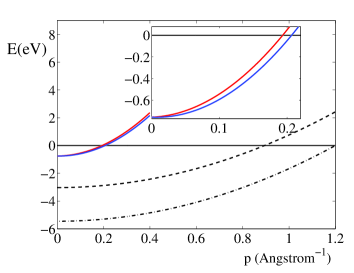
Photoemission experiments performed on (111) surfaces of gold LMJ ; NRH ; MHo ; DP ; HC reveal the existence of -gap surface Tamm-Shockley Tamm ; WS states that constitute a two-dimensional electron gas. Its properties are described by the Fermi momentum and effective mass NRH ; for comparison, the Fermi momentum for bulk electrons is . Of significant importance to us is the observation that the spin-orbit splitting of the surface states is unusually strong, which is measured to be at the Fermi level. Recent experiments CRA show that Bi/Ag(111) surface alloys can have a splitting which reaches . As we demonstrate below it is this strong spin-orbit interaction that leads to coupling of electron spin to charge oscillations via resonant electron transitions between spin-split subbands. Fig. 1 shows the energy spectrum of both bulk and surface states for Au(111).
I.1 Geometry of the system
We will consider two geometries: a) a noble metal film of thickness embedded into a insulator with a dielectric function ; b) a single metal interface with a vacuum. For the former geometry we are interested in the plasmon-polariton spectrum, while the geometry b) is discussed in relation to the observation of the surface state resonances in the reflection coefficient (or impedance) of electromagnetic radiation incident on the surface.
Both geometries require first that we analyze the dynamic response of both surface and bulk electrons. The latter are conventionally described by the Drude dielectric function
| (4) |
where the bulk plasma frequency in gold is . The electron momentum relaxation rate is typically much smaller and depends on temperature (phonon scattering) and crystal quality (impurities). Expression Eq. (4) is the approximation that neglects vacuum contribution and -band electrons. However, the resonant phenomena addressed in our paper occur at infrared frequencies, . At these frequencies the -band contribution is large and dominant, and Eq. (4) to be a good approximation.
The Hamiltonian of the surface states
| (5) |
describes the in-plane dynamics of confined electrons, with the effective spin-orbit coupling constant given by the average of Eq. (3) over the direction perpendicular to the surface (),
| (6) |
where is the wave function of a surface state. We make an approximation (consistent with the photoemission data) that is momentum-independent. The numerical value of is related to the observed value of spin-orbit splitting according to .
II Dynamic response of surface states
Qualitatively, the interaction of the electromagnetic field (plasmon, infrared beam reflected from the surface, etc.) with our system can be understood as follows. An electric field along the -direction causes charge oscillations of both bulk and surface electrons and an induced electric current . It is the resonant contribution to this current from the interband 2D transitions which is of the most interest to us here. The result of the appearance of the electric current is two-fold:
i) According to Ampere’s law, a magnetic field along the -direction appears that leads to the interface Zeeman magnetization .
ii) As seen from Eq. (5) a drift along the -direction can be considered as effective “Zeeman” field pointed along the -direction. Consequentially, it induces additional net electron spin polarization and, hence, magnetization E .
Subsequently, the surface magnetization and the accompanying ac magnetization induce an additional ac electric field (along the -direction) via Faraday’s law which acts upon both bulk and surface electrons. It is crucial that all these effects are resonantly enhanced for frequencies near the frequency of inter-subband transitions, .
Let us now address the problem of dynamic response of 2D electron states quantitatively. Most simply it can be done by means of a kinetic equation. Due to the spin structure of the Hamiltonian (5), the electron distribution function is a matrix in spin space. The corresponding equation for in the presence of both ac electric and magnetic fields has the form Ref. MH, ,
| (7) |
where , , with being the direction of electron momentum and the set of Pauli matrices; is the Bohr magneton and is the gyromagnetic ratio of surface electrons.
A formal solution to the equation (7) in the frequency domain reads (see Appendix A for more details)
| (8) |
where denotes the right-hand side of Eq. (7). To the linear order in the fields and it is sufficient to utilize the equilibrium distribution function in the right-hand side of Eq. (7), , with denoting the Fermi-Dirac functions for the two spin-split subbands.
Using Eq. (8) it is now starightforward to calculate the surface magnetization , and current density . Note that the electron velocity contains spin operator. After momentum integration we obtain for the 2D electric current and magnetization,
| (9) |
Here we explicitly emphasized that the fields are to be taken at the interface () (see also the discussion in the next section.) Here the electric conductivity of surface states (),
| (10) |
where is the density of 2D electrons, consists of the usual intrasubband Drude conductivity (first term) and the contribution of resonant intersubband transitions (second term). The dynamic magnetic susceptibility also features a similar resonant structure, which with the help of Eq. (8) is found to be
| (11) |
Finally, the cross-susceptibility has the form,
| (12) |
Note that the off-diagonal terms in Eqs. (II) are related to each other, in agreement with the Onsager theorem.
III Impedance of Au(111) surface
The most straightforward way to observe resonances, Eqs. (10)-(12), associated with the intersubband transitions is to measure the reflection of the electromagnetic wave incident from vacuum on a surface of a bulk metal. Since typical photon momenta is considerably smaller than the characteristic 2D electron momentum scales of the problem, and , it is sufficient to consider a case of normal incidence and reflection. Assuming the incident wave has frequency and amplitude , we can write the electric field as
| (13) |
Accordingly, the magnetic field is found from Maxwell’s equations. Inside the metal it reads ; and similarly in the vacuum (where ). As a result,
| (14) |
Boundary conditions relate the discontinuities of the fields and to the surface current and magnetization given by Eqs. (II),
| (15) | |||
| (16) |
The right-hand side of the boundary conditions (15) are not well defined as the surface electric current and magnetization, Eqs. (II), are given in terms of electric and magnetic fields right at the surface. The latter, however, are discontinuous at . This means that the response of surface electrons has to be in principle found from a solution of a three-dimensional problem which accounts for the -dependence of the electron density distribution, dynamics of surface states, as well as Maxwell’s equations in a self-consistent way. Such analysis is well beyond the scope of the present paper and should be a subject of a separate work. In this paper we adopt a phenomenological approach and approximate that the 2D electron density is constant across the interface so that that the effective surface electric and magnetic fields in Eqs. (II) are given by the corresponding mean arithmetic values of the magnitude of the fields immediately above and below the surface,
| (17) |
In Appendix B we show how these boundary conditions follow from the approximation of 2D electron density constant across the interface. Equations (15) together with (II) and (17) now give a system of two coupled linear equations for and . The experimentally measurable quantity, surface impedance , is given by the ratio of the electric and magnetic fields at ,
| (18) |
After simple calculation we obtain
| (19) |
Substituting now the values of , and found in the preceding section we observe that the doubly-resonant terms, , are exactly canceled by the corresponding contributions from the terms . Of the remaining terms only the -term in the denominator is to be kept, as the -terms are small by virtue of ,
| (20) |
The resonant feature in Eq. (20) is rather narrow though sharp. A finite electron scattering rate leads to its broadening.
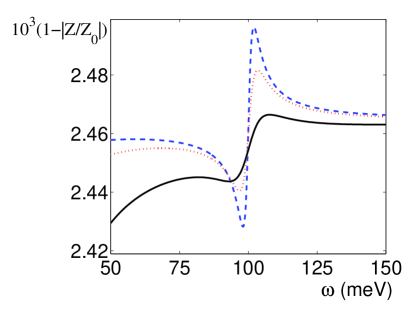
III.1 Electron scattering
The scattering of surface electrons off phonons, impurities and surface roughness can be be accounted for by a collision integral in the kinetic equation (7). In a relaxation time approximation this yields the substitution in the response functions (10)-(12). The broadening of the bulk electron response is accounted for by the imaginary part in the dielectric function (4). For estimates we will assume that the scattering rate is the same for bulk and surface states. Fig. 2 illustrates the dependence of the absolute value of the impedance close to the resonant frequency for different values of the scattering rate. Typical scattering rates in noble metals at room temperature are . In order to achieve the desired scattering rate of order one should make measurements at low, , temperatures. Due to the screening from bulk electrons, which gives large values for the refraction index , the relative correction to the surface impedance is small but within the capabilities of modern optical detection methods.
An alternative setup for the observation of intersubband surface resonances is the measurement of the transmission coefficient through a thin metal film, rather than of a reflection (impedance) from a bulk metal. The corresponding calculations can be performed in complete analogy to the above analysis.
Finally, we note that the applicability of the linear response close to the resonance requires that the first-order variation of the electronic distribution function is small compared with the equilibrium Fermi-Dirac distribution. Estimating the right-hand side of Eq. (8) we obtain that close to the resonance the following condition should be satisfied, . This condition has a simple physical meaning – the energy acquired over the spin-orbital distance in the electric field should be smaller than the detuning to the resonance or the scattering rate.
IV Plasmon spectrum of a metal film
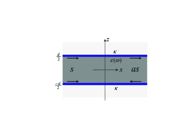
We now consider the role of intersubband resonances on the properties of plasmons in thin Au(111) films, embedded into a dielectric, see Fig. 3. The plasmon is propagating along the -direction. In general, it is accompanied by , components of electric field as well as an component of magnetic field. As illustrated in Fig. 3 there are two modes in a film, corresponding to symmetric and anti-symmetric alignment of the electric field near the two surfaces.
Let us begin by estimating the relative importance of the two resonant contributions, arising from the surface electric current and surface magnetization, cf. Eqs. (II). Integrating Faraday’s law, , across an interface, we can obtain that the additional electric field induced by the oscillating surface magnetization is . Similarly, according to Ampere’s law the additional contribution to the magnetic field due to the surface current is , where of interest is the second (resonant) term in Eq. (10). Consequentially, this magnetic field yields an additional electric field given by , for a wave with the wavevector along the -direction. Thus, the relative magnitude of the two effects is
| (21) |
where in the last identity we made use of Eqs. (II) and the response functions (10)-(12). To obtain a numerical estimate of the ratio in Eq. (21) it is sufficient to utilize the plasmon spectrum for (see Eq. (29) with the first two terms only). At low frequencies, much less than the plasma frequency, , we find, . We thus obtain,
| (22) |
As seen from this expression, smaller values of spin-orbit splitting favors the role of magnetization. At present we do not know the gyromagnetic ratio of surface electrons. For and we estimate for Au(111). The effect of the electric current is thus considerably stronger than the effect of magnetization. For thin films the suppression of is even more noticeable. Yet, assuming that in some other materials the situation can be different, in the following we analyze both contributions.
For a plasmon wave propagating along the direction, the electric field obeys the wave equation, which inside the film () has the form,
| (23) |
where the dielectric function is still given by Eq. (4). The corresponding wave equation outside the film has the same form as Eq. (23) with . Since equation (23) is invariant under spatial inversion transformation, , its solutions are either symmetric or anti-symmetric under this inversion. The symmetric solution can be written as
| (24) |
where and . The anti-symmetric solution can be written in the same manner only with the change, .
The magnetic field is found similarly to how it is done in Sec.IV and reads
| (25) |
The boundary conditions relate the discontinuity of the electric field to the interface magnetization
| (26) |
and the discontinuity of the magnetic field to the surface current,
| (27) |
cf. Eqs. (15). As already pointed out in Sec. III, the right-hand sides of boundary conditions (26-27) are not well defined as the interface current and magnetization (II) have been calculated under the assumption that the electric and magnetic fields are uniform across the interface. Adopting the same approximation as utilized above, cf. Eq. (17), we write
| (28) |
and similarly for the magnetic field. After straightforward transformations we find the dispersion equation for symmetric plasmons,
| (29) | |||||
The spectrum of anti-symmetric plasmons is determined by the equation which is obtained from Eq. (29) by the substitution . Qualitatively, the modification of the spectrum of low-frequency anti-symmetric modes is similar to that of symmetric modes though quantitatively smaller. Below we discuss symmetric plasmons only.
The first two terms in Eq. (29) describe conventional plasmons in a metallic film surrounded by a dielectric. For and they yield a well-known surface plasmon dispersion relation . The third term originates from the electric response of Tamm-Shockley surface electrons and contain an intrasubband Drude term as well as an intersubband resonant contribution, cf. Eq. (10). Finally, the last term describes the magnetic response of surface states, which also features interband resonances at , see Eq. (11). As can be easily verified, the relative magnitude of magnetic and electric 2D responses is indeed controlled by the above parameter, Eq. (22).
At low frequencies, , and the dielectric function is . Since wavelengths of interest are small, , after simple transformations (neglecting the last term in Eq. (29), which is typically a good approximation), we find a plasmon spectrum in the form,
| (30) |
Here we assumed that scattering rate is small compared with frequency and retained it in the resonant intersubband term only. For thin films, , which for Au means that , the electric field is almost uniform across the film, so that oscillations of surface electron density simply add to the oscillations of the charge density in the bulk of the film.
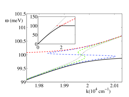
Fig. 4 illustrates the effect of the interband spin resonance on the plasmon spectrum of thin Au(111) films. Near the point where this spectrum intersects the spin resonance frequency, , there is a significant decrease in the plasmon group velocity, , and even a narrow region of negative group velocity. In addition, at the plasmon phase velocity is increased significantly and (in the absence of electron scattering) reaches the value of , characteristic of photon propagation in the dielectric. The corresponding increase of the wavelength due to the resonant interaction with surface electrons can be quite significant, as seen from Fig. 4. A finite scattering rate makes these features less sharp, but broadens them, which could in fact help their observation. However, the scattering rate should be made rather small, which emphasize the use of low temperatures.
V Plasmon spectrum of a metal film embedded in an ionic dielectric
Another interesting manifestation of the surface states can be achieved if the material surrounding the metal film is an ionic crystal. (Here we assume that the presence of a dielectric, while possibly changing the value of , does not suppress it significantly.) As well-known, the dielectric function of an ionic crystal AM ,
| (31) |
has a pole at the frequency of the transverse optical phonon and a zero at the frequency of the longitudinal optical phonon . Since the dielectric function is negative within the frequency range, , the plasmon (or, more accurately, plasmon-polariton) excitations normally cannot propagate in this range of frequencies. This can be verified from Eq. (29) with , as the first two terms in this equation are negative.
However, the finite spin-orbit splitting can change this situation dramatically if the splitting energy falls within the forbidden frequency band, i.e. . For a Au(111) film with such a situation can be realized, in particular, for LiH, , , or SiC, , , , data from Ref. K, . Since the resonant term in Eq. (10) changes sign below , plasmon-polariton modes can propagate in the bandgap with a frequency close to the frequency of intersubband transitions.
For thin films the bandgap resonance is at
| (32) |
The impedance of the coated film can be obtained similarly to the calculations of the preceding Sections. We assume here that the thickness of the insulator coating is smaller than the decay length of electromagnetic field in the insulator, . The impedance is then found to be
| (33) |
We obtain that the width of the resonance is given by the scattering rate and its relative amplitude is proportional to the ratio of the second term in Eq. (33) and the scattering rate. For the metal film of thickness and scattering rate the relative hight of the resonance will be .
Let us emphasize again that the advantage of a set-up with a polar dielectric coating lies in the fact that the resonance (32) is purely due to the intersubband transitions with no other excitations existing in the same frequency domain that could otherwise obscure their observation.
VI Summary and conclusions
Noble metals, such as Au or Bi/Ag alloys, possess the unique property that a substantial density of two-dimensional surface (Tamm-Shockley) states is present when the surface is grown in a particular direction (111) of a cubic lattice. This allows the study of the interplay of 2D and bulk 3D electron liquids. Of particular significance is the fact that the surface confining potential breaks spatial inversion and leads to an intrinsic, i.e. independent of any disorder potential, spin-orbit interaction. The latter results in the formation of spin-split surface subbands with the splitting reaching a quite significant magnitude of at the Fermi level.
The response functions of the surface states have a resonant character for frequencies close to the energy of spin-orbit splitting. This resonance allows optical detection of 2D states, which are otherwise obscured by a much large number of bulk electrons. In thin films the optical response can be expected to be influenced by the presence of surface to a larger extent. Measurements of reflection and transmission coefficients in the infrared spectrum should be able to reveal the intersubband resonances.
Another phenomenon, which is predicted to bear the signature of Tamm-Shockley states, is associated with surface plasmons, i.e. collective excitations of electron density. Surface plasmons (as well as symmetric plasmons in metal films) are gapless at long wavelengths. This ensures that the plasmon energy intersects the energy of spin intersubband resonances at some wavelength. The electric field is then strongly enhanced by the motion of 2D electrons which results in significant and detectable modifications of the plasmon spectrum.
Acknowledgements.
We acknowledge fruitful discussions with J. Gerton, V. Podolsky, M. Raikh, T. Shahbazyan, A. Shytov, and O. Starykh. The work was supported by DOE, Award No. DE-FG02-06ER46313.Appendix A Solution of kinetic equation
To solve kinetic equation (7) written in the frequency representation as
| (34) |
we first calculate its commutator with ,
| (35) |
where we utilized that . Finally, we need one more equation, which is found from Eq. (34)
| (36) |
Formally, the system of three equations (34-36) contains three unknowns: , and . Eliminating the last two of these unknowns we obtain the solution of kinetic equation in the form, Eq. (8).
Appendix B Boundary conditions
Let us assume that the amplitude of the electromagnetic field acting on surface electrons is small compared with the atomic fields (this is a rather weak condition). The modification of the electronic wave function can then be neglected and the effective electric field in Eq. (7) acting on surface electrons is written as
| (37) |
where is the wave function describing transverse confinement of surface states. Here we adopt the simplest approximation that is momentum-independent and constant across the interface layer of thickness . Equation (37) then gives,
| (38) |
The interface layer can now be considered as a metal film with the effective dielectric function
| (39) |
that is obtained from Eq. (10): is 2D density of surface electrons. Solution of Maxwell’s equation for , which satisfy the condition that and , is
| (40) |
where . As a result, Eq. (38) gives the effective field,
| (41) |
This condition reduces to
| (42) |
used throughout the paper as long as . This condition is satisfied as long as
| (43) |
References
- (1) H.A. Atwater, Sci. Am. 296, 56 63 (2007).
- (2) S.A. Maier, Plasmonics: Fundamentals and Applications (Springer, New York, 2007).
- (3) M.L. Brongersma and P.G. Kik (Edts.) Surface Plasmon Nanophotonics (Springer, Dordrecht, 2007)
- (4) D. Pines and P. Nozieres, The Theory of Quantum Liquids (Benjamin, New York, 1966).
- (5) Y.Y. Teng and E. Stern, Phys. Rev. Lett. 19, 511 (1967); R. Fuchs and K.L. Kliewer, Phys. Rev. B 3, 2270 (1971).
- (6) H. Raether, Surface Plasmons on Smooth and Rough Surfaces and on Gratings (Springer-Verlag, Berlin, 1988).
- (7) F. Stern, Phys. Rev. Lett. 18, 546 (1967).
- (8) F.T. Vas’ko, JETP Lett. 30, 540 (1979); Yu.A. Bychkov and E.I. Rashba, J. Phys. C 17, 6039 (1984).
- (9) J. Nitta, T. Akazaki, H. Takayanagi, and T. Enoki, Phys. Rev. Lett. 78, 1335 (1997).
- (10) L.I. Magarill, A.V. Chaplik and M.V. Éntin, JETP 92, 153 (2001).
- (11) X.F. Wang, Phys. Rev. B 72, 85317 (2005).
- (12) S. LaShell, B. A. McDougall, and E. Jensen, Phys. Rev. Lett. 77, 3419 (1996).
- (13) G. Nicolay, F. Reinert, S. Hüfner, and P. Blaha , Phys. Rev. B 65, 33407 (2001).
- (14) M. Hoesch, M. Muntwiler, V. N. Petrov, M. Hengsberger, L. Patthey, M. Shi, M. Falub, T. Greber, and J. Osterwalder, Phys. Rev. B 69, 241401(R) (2004).
- (15) D. Popović, F. Reinert, S. Hüfner, V. G. Grigoryan, M. Springborg, H. Cercellier, Y. Fagot-Revurat, B. Kierren, and D. Malterre, Phys. Rev. B 72, 045419 (2005).
- (16) H. Cercellier, C. Didiot, Y. Fagot-Revurat, B. Kierren, L. Moreau, D. Malterre, and F. Reinert, Phys. Rev. B 73, 195413 (2006).
- (17) I. Tamm, Physik. Zeits. Sowjetunion 1, 733 (1932).
- (18) W. Shockley, Phys. Rev. 56, 317 (1939).
- (19) C.R. Ast, J. Henk, A. Ernst, L. Moreschini, M. C. Falub, D. Pacilé, P. Bruno, K. Kern, and M. Grioni , Phys. Rev. Lett. 98, 186807 (2007).
- (20) This effect for a dc electric field was first described by V.M. Edelstein, Solid State Commun. 73, 233 (1990).
- (21) E.G. Mishchenko and B.I. Halperin, Phys. Rev. B 68, 045317 (2003).
- (22) N.W. Ashcroft and N.D. Mermin, Solid State Physics (Holt, Rineheart and Winston, New York, 1976)
- (23) Ch. Kittel, Introduction to Solid State Physics (Willey, Hoboken, 1995, 7th ed.)