Fabrication of Magneto-Optical Atom Traps on a Chip
Abstract
Ultra-cold atoms can be manipulated using microfabricated devices known as atom chips. These have significant potential for applications in sensing, metrology and quantum information processing. To date, the chips are loaded by transfer of atoms from an external, macroscopic magneto-optical trap (MOT) into microscopic traps on the chip. This transfer involves a series of steps, which complicate the experimental procedure and lead to atom losses. In this paper we present a design for integrating a MOT into a silicon wafer by combining a concave pyramidal mirror with a square wire loop. We describe how an array of such traps has been fabricated and we present magnetic, thermal and optical properties of the chip.
Index Terms:
Atom chips, Electrophoretic resist, Magneto-optical traps, Cavity patterning.I Introduction
Atom chips are microfabricated devices that control electric, magnetic and optical fields in order to trap and manipulate cold atom clouds [1], [2], [3], [4] and to form Bose-Einstein condensates [5], [6], [7]. Potential applications include atomic clocks [8], atom interferometers [9], [10], and quantum information processors [11], [12]. Silicon is one of several materials used as a substrate for atom chips. It is attractive for this purpose because its properties are well-known and fabrication techniques are highly developed. The small scale of microfabricated current-carrying wires makes it easy to generate strong magnetic field gradients near the surface of the chip, forming tight traps for paramagnetic atoms. The loading of such magneto-static traps usually starts with a magneto-optical trap (MOT) typically some 3-4 mm from the surface. This collects atoms from a tenuous, room-temperature vapour and cools them, typically to 100 K, using circularly polarised light beams in conjunction with a spherical quadrupole magnetic field. The atoms are sometimes further cooled to a few tens of K using optical molasses, before being captured in a weak magnetic trap to form a large atom cloud, typically 1 mm in size. At this point, the atoms still have to be handed over to the microscopic magnetic traps on the chip, a process that involves further compression of the cloud and very accurate positioning of the atoms. This sequence of loading and transfer is complicated and could be largely eliminated if the MOT were integrated into the chip. Moreover, integration would open up the possibility of building arrays of MOTs to prepare large numbers of independent cold atom clouds.
This paper describes the fabrication and initial testing of an integrated array of MOTs on an atom chip, as proposed by Trupke et al. [13]. Each of these MOTs automatically prepares all the required light beams from a single circularly polarised input beam by reflecting the light in a concave square pyramid of mirrors [14]. This greatly reduces both the number of expensive optical components needed to prepare the light beams and the amount of laser power needed. Integrated wires encircling the opening at the base of the pyramid produce the required magnetic field distributions with modest electrical power consumption and accurate positioning. The fabrication of an integrated MOT array on a chip represents an important step towards a truly integrated atom chip for portable applications.
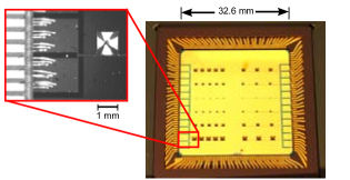
The atom chip we have fabricated has 6 rows of pyramids, ranging in size from 200 m to 1200 m, serviced by 12 separate wires to produce the magnetic fields. For pyramids up to 600 m, the encircling wires have a width of 25 m. The larger pyramids are serviced by wires of 50 m width. In total there are 48 pyramid MOTs. The whole chip is packaged into a ceramic pin grid array (CPGA) with multiple wire bonds to bring high currents in and out of the chip. The silicon sidewalls of the pyramids are coated with gold to create micro-mirrors for reflecting the laser light. The pyramids formed by etching silicon have a 70.5o apex angle, rather than the ideal 90o. The optical properties of such a pyramid have already been investigated in [13]. In those experiments it was observed that light reflected near the diagonal edges can prevent the MOT from working. Here we have developed the necessary fabrication steps to eliminate these reflections by removing the gold near the corners of the pyramids.
II Principle of the MOT on a chip
Circularly polarised light, incident along the axis of a square pyramid, is reflected by the four metal mirrors that form the pyramid. At each reflection the helicity of the light is reversed. If the pyramid has a 90o angle between opposite faces, these reflections produce three counter-propagating pairs of light beams that are mutually orthogonal. Together with a magnetic quadrupole field, this configuration creates a MOT, whose radiation pressure forces cool and trap atoms from a room-temperature vapour [14], [15].
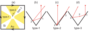
We form the pyramids by etching a silicon wafer, cut on the {100} plane. Potassium hydroxide (KOH) etches anisotropically through square openings to reveal the {111} planes, which form hollow pyramids with apex angle . This departure from a right angle causes the beams to be reflected into a variety of directions. We classify these beams as Type 1, 2, or 3, according to the region of the pyramid where the first reflection occurs, as shown in Fig. 1a. Type-1 rays are reflected on two opposite sides of the pyramid before leaving, as illustrated in Fig. 1b. Type-2 rays also reflect on opposite faces, but strike the original face again before leaving, as shown in Fig. 1c, making a total of three reflections. After the first reflection in Fig. 1d, type-3 rays head towards the opposite face, but because they are incident close to the diagonal edge of the pyramid, they are intercepted on the way by the adjacent face. Here they undergo a grazing reflection, marked (2) in the figure, where the helicity of the light is reversed. Finally, the opposite face is reached for a third reflection.
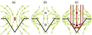
The wires electroplated on our chip form a square loop of side around the pyramid base. A current in this loop makes a magnetic field as shown in Fig. 2a. At the centre of the loop, in the plane of the wire, the field points downward with a magnitude of . We superpose a uniform vertical bias field in order to create the quadrupole field configuration required by the MOT, as shown in Fig. 2b. The strength of this bias is chosen to centre the quadrupole halfway between the base and the apex, at a distance from the surface of the chip. This requires . The light beams needed to create the magneto-optical trap inside the pyramid are formed from the incoming circularly polarised beam by the first and second reflections of the type-1 rays, as shown in Fig. 2c. The type-2 rays produce a slight imbalance in the MOT force, but are largely unimportant. The type-3 rays tend to destabilise the MOT because they have the wrong helicity and produce a strong force that pushes the atoms out of the pyramid instead of trapping them.
We have conducted preliminary experiments using a large, glass pyramid coated with gold. Initially, this failed to produce a MOT because of the presence of the type-3 rays. Atoms were successfully trapped once the gold was removed from the areas where the type-2 and type-3 rays are produced. We were also able to make the MOT operate [13] by using a lower-reflectivity (78%) coating of aluminium, which was not cut away at the edges and centre. In such a pyramid, the intensity of the harmful type-3 light is decreased relative to the type-1 beams, because of the additional reflection by the lossy surfaces.
The current in the wire determines the vertical gradient in the MOT, which is related to the corresponding bias field according to . Under typical operating conditions used in most MOT experiments, the gradient is approximately 0.15 T/m. This is readily achieved on the chip because of the small scale: for example in the 1 mm loop it requires 0.1 A. The same wires can also be used to create a purely magnetic trap, with a depth of , where is the magnetic moment of the atom. Such a trap can hold atoms for many seconds provided its depth exceeds the temperature of the atoms by a factor of 5 or so. Ideally, we would like to be able to hold a K cloud, which requires a 0.7 mT bias field, corresponding to a current in a 1 mm loop of 1 A. The feasibility of using such currents is discussed more fully in Sec. IV-B. Further details about magnetic trapping of neutral atoms can be found in Ref. [1].
In summary, the aims of the fabrication were to create pyramidal micro-mirrors which would not reflect the damaging type-3 beams, and to surround these mirrors with wires able to create the required magnetic field strengths and gradients. In the following sections we describe how these aims have been achieved.
III Fabrication
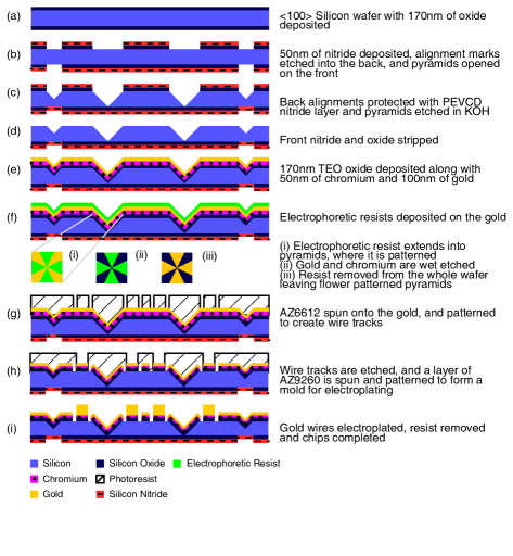
The fabrication processing sequence is shown in Fig. 3. We start by preparing the wafer and etching the pyramids. The whole surface is then coated with gold and patterned to remove the gold from the type-3 regions and to form the wire tracks. In these steps, the main fabrication challenge was to cover the wafer with a uniform resist layer, because the pyramid openings in the surface impeded the flow of the resist during spinning. Finally, the wires are electroplated to make them thick enough to carry the required current. These processes are described in more detail in the next three sub-sections.
III-A Wafer preparation and pyramid etch
The process begins with a 4 inch, 1mm-thick silicon wafer cut on the {100} plane. This is given a standard RCA and fuming nitric acid clean. A 170 nm-thick layer of silicon dioxide is grown by wet oxidation in a furnace at 1000 C (Fig. 3a). Subsequently a 50 nm layer of low stress silicon nitride is deposited on both sides by LPCVD. A reactive ion plasma etch is then used to make alignment marks on the back side of the wafer for accurate positioning of all the masks used in the fabrication process.
In order to make the pyramids, a 1 m layer of photo resist AZ6612 is spun onto the wafers. An array of square openings is patterned into the resist using a photo mask on a Karl Suss MA8 contact mask aligner. The silicon nitride and dioxide layers are removed through these openings using a dry plasma etch and the resist is then stripped in a plasma asher (Fig. 3b). Before etching the silicon, the backside alignment marks are protected by depositing a layer of PECVD silicon nitride 1m thick and the wafer edges are protected by PTFE tape. The wafer is then etched for 19 hours in KOH at a concentration of 33% by volume and at a temperature of 80 C. This produces pyramidal pits bounded by the four most slowly etched surfaces , , and (Fig. 3c). The faces of the pyramids are very smooth because of the layer-by-layer etching mechanisms involved [16] and have been shown to have rms surface roughness as low as 0.5 nm [13]. The wafers are once again cleaned in a fuming nitric acid bath before the remaining silicon nitride is stripped from the front by a dry plasma etch and the remaining silicon dioxide is removed in an HF dip (Fig. 3d). Finally, the whole front surface is covered with a plasma-enhanced TEOS oxide layer, 170 nm thick. This is to provide electrical insulation between the silicon and the metallic coating that comes next.
III-B Metallic coating and flower patterning
The metal coating consists of 50 nm of chromium and 100 nm of gold, evaporated onto the front of the wafer (Fig. 3e). In order to make the flower pattern on the faces of the pyramids, we require them to be covered by a uniform layer of resist. Spinning the resist at this stage does not produce a uniform layer because of the large depth of the pyramidal pits. In order to avoid this problem we use electrophoretic deposition of Eagle 2100 negative photo resist. The wafer is placed in the resist bath and heated to 33 C, where it acts as a cathode at -125 V. It remains in the bath until the current drops to zero, then it is rinsed in de-ionised water and dried in a vacuum oven at 65 C. At this point, the resist remains tacky, so the wafer is dipped into Eagle 2002 topcoat for 30 seconds and again dried in the vacuum oven. This method leaves a highly uniform layer of resist over the complex topography (Fig. 3f).
Next, the wafer is exposed to ultraviolet light for 77 s at 6.5 mW/cm2, using a mask designed to remove the gold from the type-3 regions. This pattern is developed using Eagle 2005 developer heated to 40 C, which is sprayed onto the surface for 4 minutes. The wafer is then dipped for 1 minute in water at 80 C to remove the resist residues and to smooth the surface of the resist. It is dried in a vacuum oven and de-scummed for 3 minutes in oxygen plasma at 110 C (Fig. 3f(i)).
The exposed gold and chromium are removed by a 35 s potassium iodide etch, followed a 5 s chrome etch (Fig. 3f(ii)). The wafers are then sprayed for 15 min to strip the resist with Eagle 2007 remover at 50 C, and placed in an asher for 1 hr at 600 W and 110 C (Fig. 3f(iii)). This process leaves a flower pattern on the gold inside each pyramid, as shown in Fig. 4. This scanning electron microscope image shows that the gold has been removed in the diagonal and central regions corresponding to the type-2 and type-3 areas illustrated in Fig. 1a. We found that it was difficult to achieve a uniform exposure of the resist inside the pyramid. When the lower part of the pyramid (near the apex) is correctly exposed, the upper part tends to be over-exposed. The dark lines on the diagonals and the dark spot at the apex are due to residual resist. The colour of the silicon surface appears darker at increasing depth in the pyramid. We attribute this to charging of the silicon dioxide surface by electron bombardment from the SEM.
III-C Wire fabrication
The final stage of fabrication is to form the wires around the base of each pyramid, as described in [17]. First, the tracks are patterned by optical lithography on the gold coating, then the wires are electroplated to provide the 3 m thickness required for carrying the electrical current.
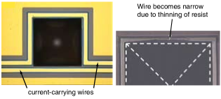
Once again, spinning a uniform layer of resist is very challenging since the radial flow is interrupted by the pyramid openings. To solve this problem we use the viscous photoresist AZ4533 as follows. A primer is spun onto the wafer to help adhesion. Then the wafer needs to be completely flooded with the resist before the spinning begins to ensure coverage inside pyramids and in the areas of the spin shadow just outside the pyramids. Spinning is carried out at 500 rpm for 10 s, followed by 30 s at 2000 rpm. We create a 5 m layer of resist, which varies in thickness by approximately 3 m where the pyramids interfere with the flow (Fig. 3g). The uniformity of the resist improves substantially around pyramids that are smaller than 1 mm, and impeccable wires are formed around the smallest pyramids, as shown in Fig. 5a. However, the thinning of the photo-resist in the spin shadow of the larger pyramids leads to overexposure and results in a thinning of the wire tracks there, as shown in Fig. 5b.
A 6 m-thick electroplating mould is then created by optical lithography of AZ9260 which is spun at 500 rpm for 8 s, followed by 30 s at 4000 rpm. This layer is exposed at 200 mW/cm2 for 30 s to create the plating mould with a minimum thickness of 3 m (Fig. 3h). The electrochemical deposition is controlled by an Autolab PGSTAT30. We use a commercial cyanide-free gold plating solution (Metalor Technologies UK, with 1 g of gold per litre of solution). A standard three-electrode setup is used with a platinum counter electrode. The deposition bath is placed in a water bath kept at 50 C and the solution is agitated throughout the deposition process using a magnetic stirrer. The current is fixed at 6 mA, corresponding to a current density of 5 mA/cm2, and the plating is run for 15 minutes to achieve a 3 m-thick gold deposit (Fig. 3i). Finally, the resist is stripped to leave the free-standing gold wires.
Electrophoresis could potentially provide a solution to the problem of the thinning of the wires. However, it can only be used when pattering the wire tracks and not when creating the electroplating mould, since the Eagle 2100 resist can only cover areas previously covered with gold. For this reason the fabrication of the wires was entirely designed and performed with the use of spin-on positive photoresists.
III-D Packaging
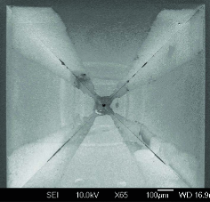
Figure 6 shows on the right an array of patterned pyramidal micro-mirrors with integrated current-carrying wires. The chip is fixed to a ceramic pin grid array (CPGA) package (CPG18023, Spectrum Semiconductor Materials Inc.) using an epoxy compatible with ultra-high vacuum (Bylapox 7285). Gold bond wires connect the package pins to the microfabricated chip wires, with 9 bond wires serving each end of a chip wire. The view on the left of Fig. 6 shows the bond wires connecting the chip to the CPGA. The ceramic package is then plugged into a pin grid array (PGA) of sockets, which in turn is soldered into an FR4 printed circuit board. This design permits a large number of connections to be made in the limited space available in the high-vacuum chamber.
We place the chip assembly in a stainless steel vacuum chamber where a 20 l/s ion pump yields a pressure below the 10-9mbar limit of our gauge after modest baking at 100 C for 2 days. At this low pressure, a trapped atom will remain undisturbed by the background gas for typically 10 s.
A stray magnetic field moves the zeros of magnetic field that form the centre of each MOT. To ensure that every pyramid encloses a field zero, we require the stray field to be less than 10 T over the chip. Much stronger fields were initially found in the recess of the CPGA where the wafer is mounted, due to permanent magnetisation of the nickel/gold coating. We therefore removed the coating by sandblasting. Immediately above the Kovar pins, there remained a stray field that reached a maximum of 10 T, but this was of short range and did not affect the 3 cm x 3 cm active area of the chip. There the field was below 500 nT, the gradients were similarly negligible, and remagnetising the assembly produced no perceptible change at that level.
IV Device characterisation
In this section we characterise the magnetic properties of our device, demonstrating that the micro-fabricated wires can carry sufficient current for magneto-optical and purely magnetic trapping. Measurements of the heating of our chip wires allow us to infer the maximum depth and gradient achievable in our trap. Finally, it is shown that the flower patterning of the pyramid coating leads to the desired suppression of type-3 beams.
IV-A Magnetic field measurements
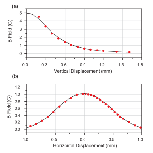
The wires around the base of each pyramid almost form a square loop, as shown in Fig. 5a. In order to calculate the magnetic field of the MOT, it is adequate to approximate this by a fully closed square loop. The solid lines in Figs. 7a and b show the vertical field component calculated for a current of 480 mA in wire 50 m wide, centred on a 895 m square. This corresponds to the geometry of the 800 m pyramid. We measured the field above this pyramid using a Hall probe (Lakeshore 421 Gaussmeter), as shown by the circles in Fig. 7. On the left is a vertical scan along the axis of the pyramid, while the scan on the right is horizontal at a height of 0.7 mm. The two are entirely consistent.
IV-B Heating tests
Although the gold wires are very good conductors, they do of course dissipate electrical energy and, at sufficiently high currents, they blow like a fuse. Considerably below that limit, the wafer heats up to 120 C. At this temperature the epoxy used to bond the silicon to the CPGA begins to decompose, losing strength and outgassing strongly, thereby compromising both the mechanical stability of the chip and the high vacuum. This limiting temperature determines the largest current that we run through the wires, and thereby limits the field and field gradient that are available.
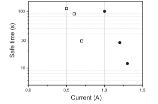
With the chip mounted and placed under moderate vacuum (10-5 mbar), we first tested how much current could be passed through individual bond wires 50 m in diameter and 2-3 mm in length. We found that these blow at approximately 1.8 A, but can survive indefinitely at 1.5 A. Since each chip pad is normally connected by 9 wires in parallel, failure of the bond wires is not a limiting factor. In order to determine the operating currents for the chip wires, we monitored the temperature of the assembly at several points using thermocouples and we monitored the temperature of the wire itself by measuring the increase of its resistance. Passing a current through the 50 m-wide chip wires, we measured the time it takes for the wire to reach 120 C, the results being shown by the filled circles in Fig. 8. In all cases the chip itself was much colder than the wire. Below 1 A, the temperature limit was never reached, but at 1.3 A, the wire approached 120 C in ten seconds. For the 25 m-wide wires, the operation was continuous below 0.5 A and was limited to ten seconds at 0.75 A, as illustrated by the open squares in Fig. 8.
Since a suitable field gradient for the MOT is 0.15 T/m, the normal operating current is 5 mA for a 200 m pyramid and 100 mA for a 1 mm pyramid. At these low currents there is negligible heating of the chip. By contrast, the 1 mm loop needs to operate at 1 A if it is to make a purely magnetic trap for a 100 K cloud of atoms. This cannot be sustained indefinitely, as shown in Fig. 8, but substantially less than one second should suffice for most practical applications. Since the field scales as , the situation is even better for purely magnetic trapping in the smaller loops.
In the course of these measurements, we found that the resistivity of the gold wire on the chip is 3.9x10-m, approximately 1.6 times higher than that of bulk gold. This is typical of electro-deposited gold. The main consequence for us is a slightly higher power dissipation than we had anticipated in our design using the book value for the resistivity.
IV-C Optical properties
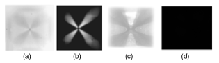
Observation of the pyramids under a microscope allowed us to check that the type-2 and type-3 reflections were indeed eliminated by removal of the gold coating to create the flower pattern. Figure 8a shows the image using unpolarized light with the microscope focussed on the apex of an unpatterned pyramid. In this figure most of the area is bright since the mirrors are reflecting light over the whole area of the pyramid. By contrast, Fig. 8b shows the same pyramid illuminated with linearly polarized light and viewed through a crossed polarizer, which suppresses all but the type-3 contribution, making the corner regions bright. Figures 8c and d show the corresponding images for a patterned pyramid. In c we see that there are no longer reflections near the apex of the pyramid, in the region of the type-2 rays. In d, we see that the removal of the gold at the edges has completely suppressed the type-3 reflections.
V Outlook
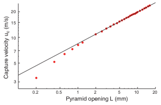
It is useful to estimate the number of cold atoms that may be captured in one of these micro-pyramids. This will depend on the usual operating variables, such as the laser detuning from the atomic transition, the positioning of the magnetic field zero, the balance of the light beams inside the pyramid and the pressure of the atomic vapour. In addition, these pyramids are at the extreme limit of small laser beam size. Normally the laser beams of a MOT are one or two centimetres in diameter, whereas these pyramids are less than a millimetre across. According to the well-established model first described by Wieman et al. [15], the number of atoms captured in a MOT is expected to scale as . Here the factor derives from the area of the laser beam, which in our case is set by the area of the pyramid opening. The quantity is the capture velocity, i.e. the speed of the fastest atoms captured by the MOT from the thermal background vapour. Using the model of Ref. [15], we have computed numerically, setting the maximum allowed stopping distance equal to the vertical height of the pyramid. The circles in Fig. 10 show the results on a log-log plot for a variety of pyramid sizes, with the laser detuning optimised separately to maximise for each size. For pyramids larger than 1 mm, we find the empirical scaling law (the solid line in Fig. 10), leading to the result . When the pyramids are smaller than that, the atom number drops a little more rapidly. We have established in a previous experiment [13] that a 16 mm pyramid made from glass blocks can capture atoms. With the help of this model, we extrapolate our 16 mm result to predict that a 1 mm pyramid will capture some atoms. The smallest pyramids on this chip, having mm, are expected by the same argument to collect approximately 25 atoms.
Although this model is a reasonable estimate, it does neglect some aspects of the full 3-dimensional geometry. For example, it assumes that the atoms of the vapour have the normal thermal distribution close to the walls of the pyramid and it neglects the polarisation gradients in the laser field, which lead to additional Sisyphus cooling [18]. Experiment will have to determine how many atoms are actually captured. The number of atoms needed depends of course on the application. At one extreme, with an array of small clouds, each containing perhaps atoms, the relative displacement of the clouds could provide a map of local magnetic field variations or be used to sense inertial forces. At the other extreme, the pyramids could serve as single-atom sources for loading integrated optical cavities, which have recently been demonstrated [19]. This would permit the production of single photons on demand for applications in quantum information processing.
VI Summary
We have fabricated a silicon chip designed to trap cold atoms in an array of integrated magneto-optical traps. The device contains 48 micro-fabricated hollow micro-pyramids surrounded by electroplated gold wires. This was packaged into a ceramic pin-grid array, and the chip’s optical and magnetic properties were tested. We found that the chip wires can easily sustain the currents needed to operate the MOTs and can even operate for many seconds at the much higher currents needed to trap atoms magnetically. The use of electrochemical deposition of photoresist allowed us to pattern a flower design on the reflective coating, a feature necessary for achieving the proper optical conditions in the magneto-optical traps. Numerical estimates show that we should be able to collect small but useful numbers of atoms in these traps, providing a simple way to feed arrays of devices on future chips. This represents an important integration step because atom chips currently have to be loaded from a single large cloud by a series of somewhat involved manoeuvres.
References
- [1] E. A. Hinds and I. G. Hughes, “Magnetic atom optics: mirrors, guides, traps, and chips for atoms”, J. Phys. D 32, 18, pp. R119-R146 (1999).
- [2] R. Folman, P. Krüger, J. Schmiedmayer, J. Denschlag and C. Henkel, “Microscopic atom optics: from wires to an atom chip”, Adv. At., Mol. Opt. Phys. 48, pp. 263–356 (2002).
- [3] J. Fortágh and C. Zimmermann, “Magnetic microtraps for ultracold atoms”, Rev. Mod. Phys. 79, pp. 235-289 (2007).
- [4] S. Eriksson, M. Trupke, H. F. Powell, D. Sahagun, C. D. J. Sinclair, E. A. Curtis, B. E. Sauer, E. A. Hinds, Z. Moktadir, C. O. Gollasch, and M. Kraft, “Integrated optical components on atom chips”, Eur. Phys J. D 35, pp. 135-139 (2005).
- [5] W. Hansel, P. Hommelhoff, T. W. Hansch, and J. Reichel, “Bose-Einstein condensation on a microelectronic chip”, Nature 413, pp. 498-501, (2001).
- [6] H. Ott, J. Fortagh, G. Schlotterbeck, A. Grossmann, and C. Zimmermann, “Bose-Einstein condensation in a surface microtrap”,Phys. Rev. Lett. 87, 230401 (2001).
- [7] C. D. J. Sinclair, E. A. Curtis, I. Llorente-Garcia, J. A. Retter, B. V. Hall, S. Eriksson, B. E. Sauer and E. A. Hinds, “Bose-Einstein Condensation on a permanent-magnet atom chip”, Phys. Rev. A 72, 03160(R) (2005)
- [8] S. Knappe, P. D. D. Schwindt, V. Shah, L. Hollberg, J. Kitching, L. Liew, and J. Moreland, “A chip-scale atomic clock based on Rb-87 with improved frequency stability”, Opt. Expr. 13, pp. 1249-1253, (2005).
- [9] Y. Shin, C. Sanner, G.-B. Jo, T. A Pasquini, M. Saba, W. Ketterle, D. E. Pritchard, M. Vengalattore and M. Prentiss, “Interference of Bose-Einstein condensates split with an atom chip”, Phys. Rev. A 72, 2 (2005).
- [10] T. Schumm, S. Hofferberth, L. M. Andersson, S. Wildermuth, S. Groth, I. Bar-Joseph, J. Schmiedmayer and P. Krüger, “Matter-wave interferometry in a double well on an atom chip”, Nat. Phys. 1, pp 57 - 62 (2005).
- [11] M. Trupke, J. Metz, A. Beige, and E. A. Hinds, “Towards quantum computing with single atoms and optical cavities on atom chips”, J. Mod. Opt. 54, pp. 1639-1655, (2007).
- [12] J. Schmiedmayer, R. Folman, T. Calarco, “Quantum information processing with neutral atoms on an atom chip”, J. Mod. Opt. 49, 8, pp.1375-1388 (2002).
- [13] M. Trupke, F. Ramirez-Martinez, E. A. Curtis, J. P. Ashmore, S. Eriksson, E. A. Hinds, Z. Moktadir, C. Gollasch, M. Kraft, G. V. Prakash, and J. J. Baumberg, “Pyramidal micromirrors for microsystems and atom chips”, Appl. Phys. Lett. 88, 071116, (2006).
- [14] K. I. Lee, J. A. Kim, H. R. Noh, and W. Jhe, “Single-beam atom trap in a pyramidal and conical hollow mirror”, Opt. Lett. 21, pp. 1177-1179, (1996).
- [15] K. Lindquist, M. Stephens, and C. Wieman , “Experimental and theoretical study of the vapour-cell-Zeeman optical trap”, Phys. Rev. A 46, pp. 4082-4090 (1992).
- [16] Z. Moktadir and H. Camon, “Monte Carlo simulation of anisotropic etching of silicon: investigation of [111] surface properties”, Modell. Simul. Mater. Sci. Eng. 5, pp. 481-488, (1997).
- [17] E. Koukharenko, Z. Moktadir, M. Kraft, M. E. Abdelsalam, D. M. Bagnall, C. Vale, M. P. A. Jones and E. A. Hinds, “Microfabrication of gold wires for atom guides”, Sens. Actuators A 115 2-3, pp 600-607 (2004).
- [18] H. J. Metcalf and P. van der Straten, ”Laser Cooling and Trapping”, Springer-Verlag New York. (1999).
- [19] M. Trupke, J. Goldwin, B. Darquie, G. Dutier, S. Eriksson, J. Ashmore, and E. A. Hinds, “Atom detection and photon production in a scalable, open, microcavity”, Phys. Rev. Lett. 99, 063601, (2007).