Effects of current on nanoscale ring-shaped magnetic tunnel junctions
Abstract
We report the observation and micromagnetic analysis of current-driven magnetization switching in nanoscale ring-shaped magnetic tunnel junctions. When the electric current density exceeds a critical value of the order of A/cm2, the magnetization of the two magnetic rings can be switched back and forth between parallel and antiparallel onion states. Theoretical analysis and micromagnetic simulation show that the dominant mechanism for the observed current-driven switching is the spin torque rather than the current-induced circular Oersted field.
I Introduction
In the experiments that demonstrated current-driven magnetization switching for spin valve pillars Ralph or magnetic tunnel junctions (MTJs) Huai , magnetic elements have been patterned into elliptic or rectangular shapes. Undesired properties such as a large shape anisotropy and a strong stray field would place a severe limitation on these magnetic elements for ultra-high density memory devices. The ring-shaped spin valve or MTJ eliminates the stray field and enhances the thermal stability since the magnetization may ideally form a vortex structure free of magnetic poles Zhu ; Chien ; Chu . Recently, the magnetic rings made of a single magnetic layer Vaz ; LiS ; Rotman and of spin valves Ross ; Ross1 ; Otani ; Zhu2 ; Chen have been achieved. For the current in the plane of the layers (CIP), the measurement of the CIP resistance of the spin valve probes the domain structure of the free layer Ross . For the current perpendicular to the plane of the layers (CPP), the magnetization can be switched by the current Otani ; Zhu2 ; Chen . In these studies, the size of the rings is ranged from sub-micrometers to micrometers and the current-induced Oersted field is the dominant mechanism in switching. To achieve the switching by the spin transfer torque Slonczewski , it is necessary to make the ring size of the order of 100nm or less. We had previously reported ring-shaped magnetic tunnel junctions Wen where the fixed layer is pinned by an antiferromagnetic layer.
In the present work, we have successfully made a series of the ring-shaped MTJ structures with various ring diameters and without an antiferromagnetic layer; this simpler layer structure makes the analysis more straightforward. Our micromagnetic simulation shows that the observed magnetization switching is originated from spin transfer torques and the current-induced circular Oersted field plays very minor roles in switching. Although the desired vortex states have not been identified in our experiments and simulation, the definitive verification of the switching between onion states (described in detail later) by the spin torque is encouraging for further exploring the geometrically controlled magnetic states.
II Experimental procedures
Multilayered MTJ films with the hard-ferromagnetic/insulator/soft-ferromagnetic layer structure of Ta(5)/Cu(20)/Ta(5)/Co50Fe50(2.5)/Al(0.7)-oxide/Co60Fe20B20(2.5)/Ta(3)/Ru(5) (thickness unit: nm) were deposited on the Si(100)/SiO2 substrate using an ULVAC TMR R & D Magnetron Sputtering System (MPS-4000-HC7) with a base pressure of Pa. The Al-oxide barrier was fabricated by inductively coupled plasma (ICP) oxidizing 0.6 nm Al-layer with an oxidation time of 10 s in a mixture of oxygen and argon at a pressure of 1.0 Pa in a separate chamber. Two electrodes situated above and below the NR-MTJ were patterned by ultraviolet optical lithography (UVL) combined with Ar-ion beam milling Zeng ; Wei . The active ring-shaped junction area was patterned by electron beam lithography (EBL) using a Raith 150 scanning electron microscope and reactive ion etching (RIE). The nanoring MTJ pillar including the top resist was then buried by SiO2 deposition. Finally, the resist and SiO2 on the top of a nanoring were removed using a lift-off process before the top electrode was patterned in the perpendicular direction.
The transport measurement was conducted via a standard four probe method. The tunnel resistance was measured by applying a small current () so that the magnetic state of the ring is not disturbed.
III Experimental Results and Micromagnetic Analysis
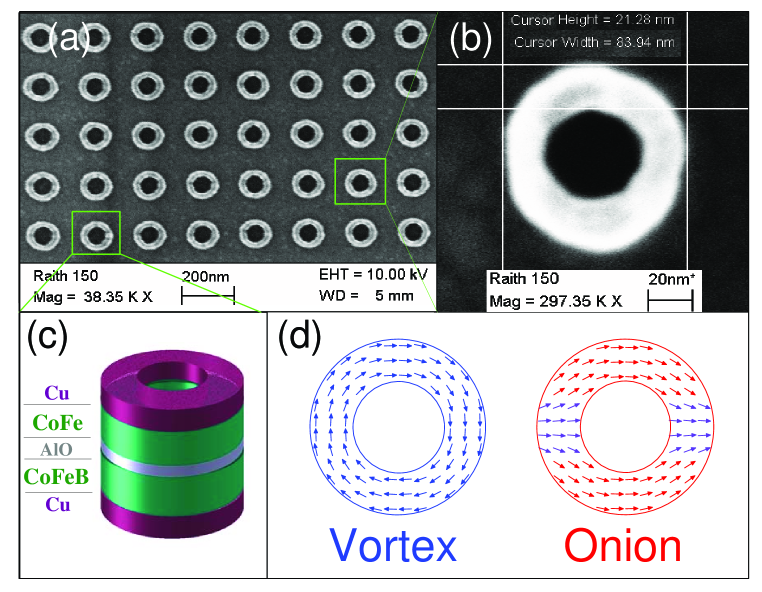
Figure 1(a-b) show the SEM images of an array of ring-shaped MTJs and of a single MTJ whose inner and outer diameters are 50nm and 100 nm, respectively. The magnetization state of a deep submicron-sized single ring has two possible stable configurations at the zero external magnetic field (remanent state): onion (O) and vortex (V) as shown in Fig. 1(d). The onion states are metastable states; they can be easily formed via the application of an in-plane magnetic field. Each onion state has a pair of domain walls; in the presence of a large uniaxial anisotropy, two domain walls are pinned around the easy axis. If the anisotropy is small, the magnetostatic interaction between two domain walls tends to attract each other, forming a slightly asymmetric onion state (not shown). The vortex state is the lowest energy state and is more stable than the O state. However, there is no simple experimental method available to produce the V state. Our micromagnetic simulation simulation shows that the transition from the onion state to the vortex state does not occur when one just sweeps the in-plane magnetic field from a large positive value to a negative one for the samples with only 2.5nm layer thickness. Instead, the two domain walls of the onion state rotate along the circumference until the polarization of the onion state is reversed. We will discuss the generation of the V state in the end of the paper.
III.1 Magnetic field driven switching
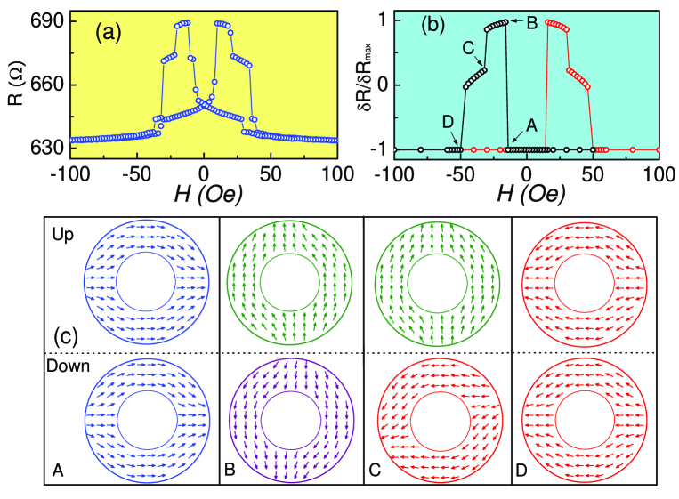
Figure 2 shows the tunnel resistance when we apply an in-plane magnetic field along the easy axis of the ring. At a large field, magnetization of both rings are in the parallel onion state and thus the resistance is lowest. When the field is reduced, the stray field of the domain walls causes the onion states of the upper and lower rings to rotate oppositely in order to reduce the magnetostatic energy. Since the anisotropy of the two layers is small, each onion state will oppositely rotate 900 to form an antiparallel configuration and the tunnel resistance becomes maximum. Further reversing the magnetic field causes the onion states of the two layers to become parallel again.
To reproduce the qualitative features of the above experimental data, we perform a numerical simulation by taking the following plausible assumptions. First, several jumps shown in Fig. 2a indicate the existence of pinning potentials and we model the pinning by simply including an in-plane four-fold anisotropic field. Second, an interlayer coupling between two rings is likely to exist for the ultra-thin insulator barrier. Thus, we have added a 60 (Oe) ferromagnetic coupling field, which is consistent with our previous experiments on similar junctions having elliptical shapes Han . Third, the tunnel conductance is calculated via the standard formulation of tunnel magnetoresistance given below
| (1) |
where () are the conductance for the two magnetic layers in parallel (antiparallel), is the area of the ring, is the angle between the local magnetization vectors and of the top and bottom rings, and denotes the in-plane coordinates. Once the magnetization states of the top and bottom rings are obtained via micromagnetic simulation, the conduction or the tunnel magnetoresistance can be readily derived from Eq. (1). As seen from Fig. 2(b), the simulated results reproduce the main shape of the experimental R-H curves.
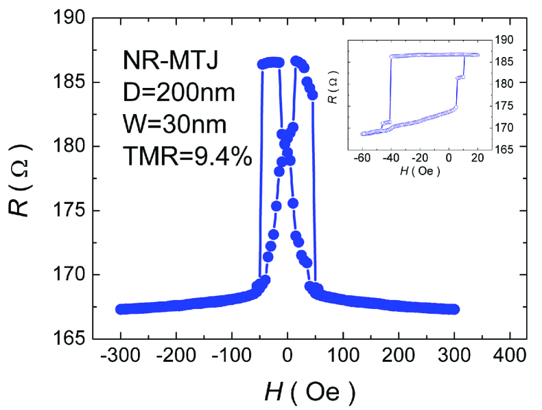
We note that there are several subtle features that are not reproduced by the simulation. First, the gradual increase of the resistance at low field observed in the experiment indicates the gradual rotation of the domain walls; the origin is likely from the competition between magnetostatic interactions of the two rings and the pinning potentials Hayward . Second, there are small sudden jumps in the resistance at low fields between the parallel resistance and the onset of the gradual increase to the anti-parallel resistance. The reason might be due to the misalignment among easy axes of two layers and the direction of the magnetic field. If we consider that the easy axes of the two layers make an angle , a large field would make the onion states of the two layers in parallel. As the field reduces to a smaller value, a transition occurs where the two onion states tend to return to their respective easy axis, i.e., forming approximately an angle . Note that this irreversible jump depends on the location of the pinning potential. We show in Fig. 3, the R-H characteristic of a similar ring where the major and minor hysteresis jumps occur in several magnetic fields. Interestingly, the inserted minor loop contains only one small jump. These uncontrolled subtle feature indicates the imperfection of the ring stucture.
III.2 Current-driven switching
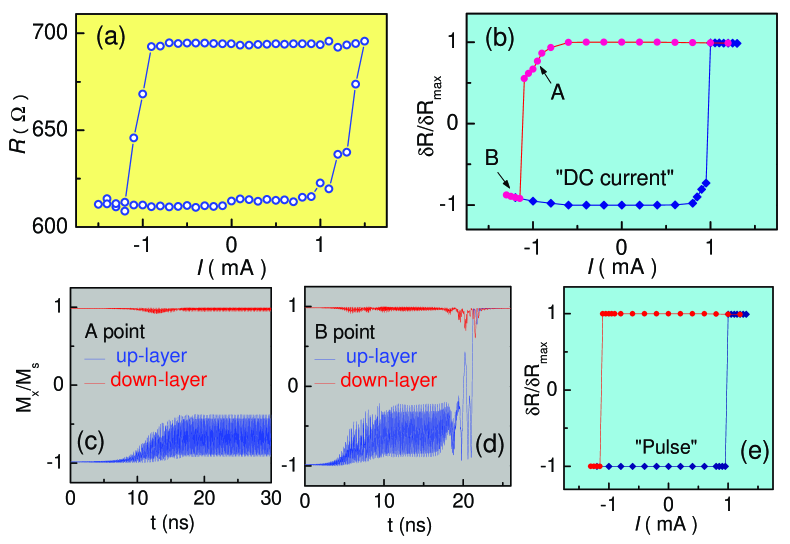
Next we show the tunnel resistance by sweeping the current at zero magnetic field. The data were recorded as follows. Before each resistance measurement, a current pulse whose amplitude and width was applied. The resistance is then measured by using a low readout current of that will not disturb the magnetic state formed after each current pulse. By repeating the above process for an increasing or decreasing amplitude of , we obtained the full R-I loop in Fig. (4). One notices that the two values of the resistance are very close to the values in Fig. 2(a), indicating that the magnetization of the two layers are two onions states with parallel (low resistance) and antiparallel (high resistance) configurations. The critical switching current from antiparallel (parallel) to parallel (antiparallel) states is about 1.1 m, which corresponds to the current density about .
Two competing mechanisms are responsible for the switching of the magnetization by the current. First, the current induces a circular magnetic field that may affect the magnetization states. However, our data suggest that the current-induced magnetic field cannot be the dominant mechanism for the switching: 1) For the current mA, the maximum Oersted field at the outer boundary of an 100nm-diameter infinite long cylinder is less than 40 (Oe); this Oersted field is clearly an overestimation since the field would be smaller for our ring structure. Simulation indicates that one needs at least several times larger current density to reverse the polarity of the onion state. More specifically, we find from micromagnetic simulation that without the spin torque the circular Oersted field is able to rotate the domain walls of the onion state by only a few degrees. 2) The measured critical current density, shown in Fig. (4a), is approximately same for different sizes of rings (not shown) while the Oersted field driven reversal Chen would be strongly size dependent. Thus we propose that the spin transfer torque is the dominant factor for the observed switching.
We have performed micromagnetic simulation by explicitly taking into account both the spin torque and the induced Oersted field. We model the spin torque on via ZLi where is proportional to the current. Figure 4(b)-(d) show the simulation results. We note that both the observed (Fig4a) and simulated (Fig4b) R-I loops does not show distinct steps (see Fig. 2); this indicates that the current driven switching is relatively insensitive to local pinnings compared to the field driven switching. We attribute this feature to the spin transfer torque: the switching current density is proportional to where is the anisotropy field and is the saturation magnetization Slonczewski . Since is much larger than and pinning potentials, the critical current is thus not sensitive to the local defects. We also notice that the simulation shows a gradual change in resistance just before switching near the parallel (anti-parallel) resistance at positive (negative) currents, while the experimental switching between parallel and anti-parallel is abrupt. This discrepancy is due to an artifact that the simulation was carried out with a constant current density. When the current is near the switching current, one of the layers is in a stable precessional state (this stable precessional state is the signature of the spin torque), see Fig. 3(c). Experimentally, the resistance was measured after the pulsed current was switched off. Therefore, the measured states returned to the parallel onion states. If we turn off the current after certain time in simulation, the loop will have no gradual change because the precessional states will return to either the parallel or antiparallel states, see Fig. 4(e).
III.3 Discussions and summary
The quantitative analysis of the spin torque effect in MTJ involves a number of key parameters. The critical current at finite temperature is given by Koch ; Li
| (2) |
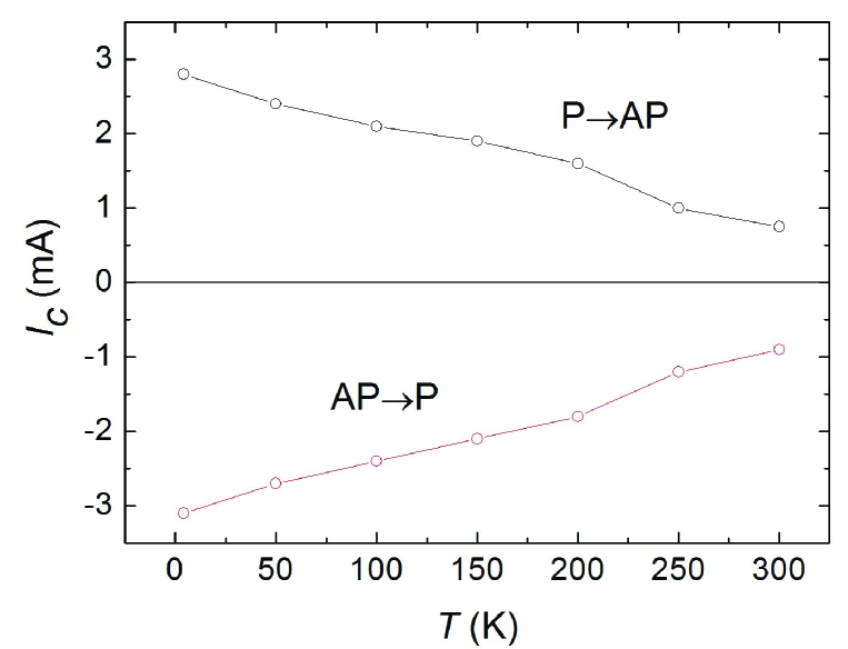
where is the intrinsic (zero temperature), is the temperature, is the energy barrier separating antiparallel and parallel onion states, ns is the pulse width of the current and /s is the attempt frequency. It is expected that the temperature will be significantly higher than the room temperature when the bias voltage is of the order of 1 V Toshiba . The energy barrier depends on the detail of the magnetostatic interaction as well as defects of the ring structure Martinez ; He . Furthermore, the recently proposed perpendicular spin torque also contributes the energy barrier SL ; Theodonis . The uncertainty of these parameters makes the quantitative comparison very difficult, if not at all impossible. We show in Fig. (5) the critical current as a function of the temperature. The significant reduction of the critical current at high temperatures implies the importance of the thermally assisted switching.
While our initial motivation for the study of ring structure is to create and switch vortex states which are robust against thermal fluctuation, we are unable to create such stable vortex states in the present experiments. A plausible interpretation is that the vortex states are topologically different from the onion states and one needs to annihilate two magnetic domains of the onion state to create a vortex state. For our ultra-thin rings, one would require a large out-of-plane rotation to convert the onion to the vortex states and thus it is energetically prohibited. One possible way to initialize a vortex state is to utilize a circular magnetic field generated by the current, but the required current density is too high. Other methods, for example, applying a large out-of-plane field along with a moderate current, might be more suitable for the initial formation of the vortex states. It is an experimental challenging problem to manipulate well-controlled vortex states in ultra thin rings. We defer this study in the future.
In summary, we demonstrate for the first time that magnetization of the ring-shaped MTJ can be switched by a current. The current density of the order of is sufficient to switch one onion state to another. This work opens a possibility for creating high-density magnetic elements with enhanced thermal stability and reduced power consumption.
This research was supported by the State Key Project of Fundamental Research of Ministry of Science and Technology (MOST), Chinese Academy of Sciences (CAS), and National Natural Science Foundation (NSFC), China. X. F. Han gratefully thanks the partial support of Outstanding Young Researcher Foundation (Grant No.50325104 and 50528101), NSFC project(Grant No.10574156), Wang Kuan-Cheng Foundation and Micro-fabrication Center of IOP from CAS. S. Zhang acknowledges the support from NSF (DMR-0704182) and DOE (DE-FG02-06ER46307) of US.
References
- (1) J. A. Katine, F. J. Albert, R. A. Buhrman, E. B. Myers, and D. C. Ralph, Phys. Rev. Lett. 84, 3149-3152 (2000).
- (2) Y. Huai, F. Albert, P. Nguyen, M. Pakala, and T. Valet, Appl. Phys. Lett. 84, 3118-3120 (2004).
- (3) J. -G. Zhu, Y. Zheng and G. A. Prinz, J. Appl. Phys. 87, 6668 (2000).
- (4) C. L. Chien, F. Q. Zhu, and J. G. Zhu, Physics Today 60, 40-45 (2007).
- (5) F. Q. Zhu, G. W. Chern, O. Tchernyshyov, X. C. Zhu, J. G. Zhu, and C. L. Chien, Phys. Rev. Lett. 96, 027205 (2006).
- (6) C. A. F. Vaz, et al., J. Phys.: Condens. Matter 19, 255207 (2007) and references therein.
- (7) S. P. Li, D. Peyrade, M. Natali, A. Lebib, Y. Chen, U. Ebels, L. D. Buda, and K. Ounadjela, Phys. Rev. Lett. 86, 1102 (2001).
- (8) J. Rothman, M. Klaui, L. Lopez-Diaz, C. A. F. Vaz, A. Bleloch, J. A. C. Bland, Z. Cui, and R. Speaks, Phys. Rev. Lett. 86, 1098 (2001).
- (9) W. Jung, F. J. Castano, and C. A. Ross, Appl. Phys. Lett. 91, 152508 (2007).
- (10) F. J. Castano, D. Morecroft, W. Jung, and C. A. Ross, Phys. Rev. Lett. 95, 137201 (2005).
- (11) T. Yang, A. Hirohata, M. Hara, T. Kimura, and Y. Otani, Appl. Phys. Lett. 90, 092505 (2007).
- (12) M. T. Moneck and J. -G. Zhu, J. Appl. Phys. 99, 08H709 (2006).
- (13) Chen, C. C. et. al. IEEE Trans. Mag. 43, 920 (2007).
- (14) J. C. Slonczewski, J. Magn. Magn. Mater. 159, L1-L7 (1996).
- (15) Z. C. Wen, H. X. Wei and X. F. Han, Appl. Phys. Lett. 91, 114102 (2007).
- (16) Z. M. Zeng, J. F. Feng, Y. Wang, X. F. Han, W. S. Zhan, X. G. Zhang, and Z. Zhang, Phys. Rev. Lett. 97 106605 (2006).
- (17) H. X. Wei, M. C. Hickey, G. I. R. Anderson, X. F. Han, and C. H. Marrows, unpublished.
- (18) Zero-temperature micromagnetic simulation is carried out by choosing the mesh size nm3 so that there are total seven meshes in the thickness dimension (the center layer is that does not have the magnetic moment) throughout the paper. A special care is taken for the edges of the rings; see M. J. Donahue, and R. D. McMichael, IEEE Trans. Magn., 43, 2878-2880 (2006).
- (19) X. F. Han, S. F. Zhao and A. C. C. Yu, Sci. Tech. Adv. Mater. 6/7, 784 (2005).
- (20) T. J. Hayward, J. Liandro, R. B. Balsod, J. A. C. Bland, D. Morecroft, F. J. Castano, and C. A. Ross, Phys. Rev. B 74, 134405 (2006).
- (21) Z. Li and S. Zhang, Phys. Rev. B 68, 024404 (2003).
- (22) R. H. Koch, J. A. Katine, and J. Z. Sun, Phys. Rev. Lett. 92, 088302 (2004).
- (23) Z. Li and S. Zhang, Phys. Rev. B 69, 134416 (2004).
- (24) M. Yoshikawa, et al., J. Appl. Phys. 101 09A511 (2007).
- (25) E. Martinez, et al., Phys. Rev. Lett. 98, 267202 (2007)
- (26) J. He, Z. Li and S. Zhang, J. Appl. Phys. 98, 016108 (2005).
- (27) J. C. Slonczewski and J. Z. Sun, J. Magn. Magn. Mater. 310, 169 (2007).
- (28) I. Theodonis, N. Kioussis, A. Kalitsov, M. Chshiev, and W. H. Butler, Phys. Rev. Lett. 97, 237205 (2006).
Figure Caption
FIG.1 The SEM images of the array a) and single b) magnetic tunnel junction rings. Schematically shown are the layers of the ring c) and two stable magnetization patterns d) of one magnetic layer at zero magnetic field (remanent states): Vortex (V) and Onion (O) states. Note that there are other equivalent states corresponding to reversing the polarity of the magnetization of the above two states.
FIG.2 The room-temperature tunnel resistance as a function of the magnetic field for a ring-shaped MTJ whose outer diameter is 100nm. b) Calculated normalized tunnel resistance where and , and and are the resistances for the parallel and the antiparallel aligned onion states of the top and bottom rings. The parameters in micromagnetic simulation are specified below: the uniaxial anisotropy of FeCo is 50 (Oe) and of FeCoB is 0 (Oe), the saturation magnetization of FeCo and FeCoB are 1130 emu/cc and 1000 emu/cc, and the interlayer coupling field is 60 (Oe). In addition, an in-plane four-fold anisotropic field of 90 (Oe) is applied to mimic the pinning potentials.
FIG.3The room-temperature tunnel resistance as a function of the magnetic field for a ring-shaped MTJ whose outer diameter is 200nm. Insert: the minor hysteresis loop.
FIG.4The tunnel resistance as a function of the amplitude of the 200ns pulsed current density at zero magnetic field. a) Experimental results at room temperature. Simulation results of the R-I loop b), the precessional states near the critical current density c) and the switched state for the current exceeding the critical vale. The same set of parameters in Fig. 2 in addition to the damping parameters of 0.01 and 0.015 for the top and bottom magnetic rings are used for the simulation. e) The simulated R-I curve after the pulsed current is turned off.
FIG.5The temperature dependence of the dc critical current density for a ring-shaped MTJ whose outer diameter is 100nm.