Current address: ] Harvard University, 12 Oxford Street, Cambridge, MA 02138
Diameter-dependent conductance oscillations in carbon nanotubes upon torsion
Abstract
We combine electromechanical measurements with ab initio density functional calculations to settle the controversy about the origin of torsion-induced conductance oscillations in multi-wall carbon nanotubes. According to our observations, the oscillation period is inversely proportional to the squared diameter of the nanotube, as expected for a single-wall nanotube of the same diameter. This is supported by our theoretical finding that differential torsion effectively decouples the walls of a multi-wall nanotube near the Fermi level and moves the Fermi momentum across quantization lines. We exclude the alternative explanation linked to registry changes between the walls, since it would cause a different diameter dependence of the oscillation period.
pacs:
81.07.De, 73.63.Fg, 85.35.Kt, 85.85.+jCarbon nanotubes Jorio et al. (2008) (CNTs) are mechanically robust and electrically conducting, and thus seem well suited for use in nanoelectromechanical systems (NEMS) Williams et al. (2002); Hall et al. (2006); Fennimore et al. (2003); Papadakis et al. (2004); Meyer et al. (2005). The electronic response of CNTs to mechanical deformations is currently a subject of high interest Joselevich (2006); Maiti (2003); Williams et al. (2002); Gómez-Navarro et al. (2006); Hall et al. (2006); Cohen-Karni et al. (2006); Hall et al. (2007). Torsion-induced conductance oscillations have been recently reported in multi-wall nanotubes (MWNTs), but their interpretation left several questions unanswered Cohen-Karni et al. (2006). To use CNTs as NEMS elements like torsional springs and gyroscopes, it is important to understand the origin of conductance changes induced by twisting the nanotube.
Here we combine electromechanical measurements with ab initio density functional calculations to settle the controversy about the origin of torsion-induced conductance oscillations in multi-wall carbon nanotubes. The first explanation, referring to a single-wall nanotube, suggests that conductance oscillations occur due to changes in the fundamental band gap, as the Fermi momentum crosses k sub-band quantization lines, shown in Fig. 1(c), while the nanotube is twisted Yang and Han (2000); Bailey et al. (2002); Cohen-Karni et al. (2006). The application to MWNTs is justified by our finding that differential torsion effectively decouples the walls on a MWNT near the Fermi level. The second explanation invokes the change in registry, as the outermost wall of a MWNT is rotated Kwon and Tománek (1998) or twisted Paulson et al. (2000); Charlier et al. (2007) with respect to the interior walls. We find the first explanation to be correct, as it predicts the conductance oscillation period to change with the inverse square diameter of the nanotube, in accordance with our measurements, rather than the inverse diameter, as suggested by the latter model.
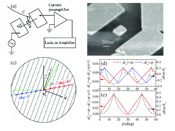
A schematic of the experiment is shown in Fig. 1(a). Figure 1(b) shows a fabricated suspended MWNT-pedal device with contacts at both nanotube ends Cohen-Karni et al. (2006). The pedal is pressed by an AFM tip, seen in the schematic, to twist the suspended nanotube. The torque and torsional strain on the nanotube and its conductance are measured simultaneously as the nanotube is twisted. Here we present results for nanotubes of different diameter to answer open questions about the torsional electromechanical response.
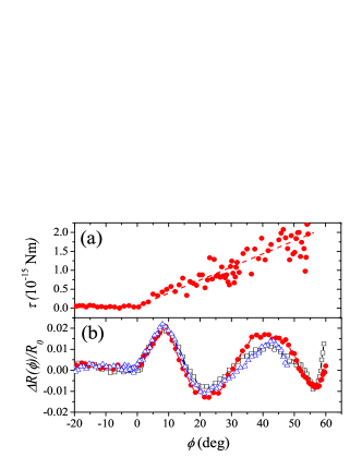
The torque experienced by the nanotube as a function of the torsion angle is plotted in Fig. 2(a). Figure 2(b) shows the oscillatory behavior in the relative resistance change as the nanotube gets twisted, with as the reference. The observed behavior is reproducible for several press-retract cycles.

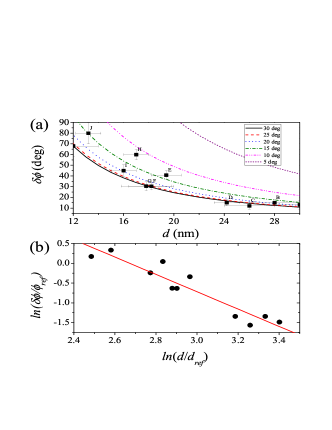
as a function of torsion angle is shown in Fig. 3 for a few representative MWNT diameters. The gradual increase in the oscillation period with decreasing nanotube diameter is evident. The oscillation period for every MWNT was obtained by taking an average from several press-retract cycles. The observed oscillation period is represented by solid squares in Fig. 4(a) as a function of the MWNT diameter .
We first examine the consequences of the shift in on the nanotube conductance. For a nanotube under torsion, the shift in relative to the invariant k lines in the circumferential direction is given by Yang and Han (2000); Cohen-Karni et al. (2006). Here is the length of the twisted section of the nanotube and is the carbon-carbon bond length. is the chiral angle or chirality of the untwisted nanotube, defined as the angle between the chiral vector and the zigzag direction on a graphene plane.
Due to the linearity of the dispersion relation near , the band gap is proportional to the distance of in the circumferential direction from the nearest k sub-band. Therefore, initially changes in a linear fashion with torsion. However, when reaches one of the lines, the band gap vanishes and further torsion causes renewed opening of the gap. The band gap reaches its maximum at the midpoint between two sub-bands, where further torsion decreases its value. Thus, the band gap oscillates between zero and its maximum value, leading to periodic metal-semiconductor transitions (M-S effect). The change in band gap with torsion is thus given by
| (1) |
where is an integer corresponding to the change in the quantum number associated with the nearest sub-band before and after twisting. Simulated for a CNT of nm is plotted in Figs. 1(d) and 1(e). Figure 1(d) shows for an initially semiconducting nanotube. Since the two halves of the CNT experience opposite torsion angles when the pedal is pressed, for each half is shown separately. Figure 1(e) shows for an initially metallic CNT, in which case the change in the band gap is the same for both halves.
The resulting from the is given by
| (2) |
where is the torsion-induced change in the activation energy, equal to . A is an attenuation factor, is the contact resistance, is Planck’s constant and and the electron charge. is the transmission probability Cohen-Karni et al. (2006) and is the initial activation energy. Thus, has the same oscillation period as . This can also be seen from Fig. 1(d) and 1(e), where is shown by the dashed lines.
For a nanotube of diameter , the sub-band spacing is . Therefore, the conductance oscillations occur with the period , which translates to
| (3) |
This equation provides the following insight:
(i) The minimum oscillation period for a nanotube of a particular diameter is given by , which is shown by the solid line in Fig. 4(a). The figure clearly indicates that within experimental error.
(ii) When a zigzag nanotube with is twisted, moves parallel to the lines, thus keeping the band gap constant. This also follows from Eq. (3), which suggests that as . However, assuming a homogeneous distribution of chiralities, we can expect % of the nanotubes to have chiralities in the range 5∘ to 30∘ and 67 to have chiralities between 10∘ and 30∘. Also plotted in Fig. 4(a) by various broken lines is the theoretical value of according to Eq. (3) for chiralities between 5∘ and 30∘. All experimental points lie in the chirality range 10∘ to 30∘. We speculate that this could simply be because the chirality distribution may not be homogeneous and higher chiralities are favored during the MWNT growth. Another possible reason is that strain-induced displacements of the triangular sublattices in graphene, known to change the band gap Nisoli et al. (2007), have been neglected. We thus expect even zig-zag nanotubes to change their conductance with torsion. This could mean that our estimated nanotube chiralities may be higher than the actual values.
(iii) According to Eq. (3), a plot of versus should give a straight line with the slope . A linear fit of these data, shown in Fig. 4(b), indicates an optimum slope of , supporting our claim that the oscillation period is proportional to .
An alternative explanation of the conductance oscillations links them to changes in registry between the nanotube walls of a MWNT as the outermost wall is twisted. This could modify the electronic coupling between the walls, causing changes in conductance. Considering only the outermost and the neighboring inner wall, the double-wall nanotube structure forms a Moiré pattern, which can be thought of as beats in two dimensions. Therefore, for a particular shear strain , the number of coincidences in the Moiré pattern varies linearly with . should then be inversely proportional to the number of these coincidences, . Since , we would expect . Our observation of a different functional dependence, , thus excludes the Moiré effect as a cause of the conductance oscillations.
In order to understand the apparent absence of the Moiré effect and justify neglecting the inter-wall interactions when determining the band gap, we performed geometry optimization and electronic structure calculations of corresponding model systems. We used the ab initio density functional theory (DFT) formalism in the local density approximation (LDA), as implemented in the SIESTA code Soler et al. (2002), with a double- basis set including polarization orbitals, and a mesh cutoff energy of 200 Ry. We used an ultra-fine -point mesh equivalent to a -point sampling of the graphene Brillouin zone, including the point. All structures were optimized until all force components on atoms were less than 0.01 eV/Å. The calculated in-layer bond length Å and the interlayer spacing Å in the optimized structure of bulk hexagonal graphite showed a deviation of no more than % from the experimental data Kelly (1981).
Before addressing twist-related changes in the transport of MWNTs, we investigate the effect of inter-wall interaction on the electronic structure of double-wall nanotubes (DWNTs), which, especially in the limiting case of very large diameters, should closely resemble that of graphene bi-layers. Since it is extremely unlikely to find DWNTs with chiral indices representing a commensurate structure of the adjacent walls, as it can be found in AA or AB stacked graphene bilayers, we will focus on the general case of incommensurate DWNT structures. The counterpart of a DWNT with incommensurate and walls is a graphene bilayer, where the upper layer has been rigidly rotated–within its plane–with respect to the layer below. Both in DWNTs and graphene bilayers, for specific rotation angles or chiral index combinations, we commonly find quasi-commensurate arrangements with large but finite unit cells, associated with Moiré patterns. With the graphene layers in a bilayer being spanned by the primitive lattice vectors and , a Moiré pattern can be produced by rotating the initially coinciding layers about one site so that the lattice point in the upper layer aligns with the lattice point in the lower layer.
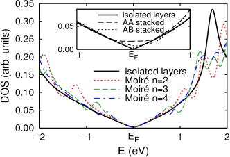
In Fig. 5 we compare the density of states (DOS) of a graphene monolayer to that of AA and AB stacked bilayers and bilayers forming Moiré patterns with . Our results show that a graphene monolayer is a zero-gap semiconductor, whereas commensurate AA or AB bilayers are metallic. The cause is the finite inter-layer coupling, combined with the favorable symmetry in the latter systems, which introduces new states near . Due to the lack of such symmetry in graphene bilayers forming Moiré patterns, we find no signature of the inter-layer coupling in the electronic structure near the Fermi level. As seen in Fig. 5, the electronic density of states of such incommensurate structures is nearly identical to that of isolated graphene monolayers. This finding holds even in view of the inter-layer interaction and distance, which undergo a modulation of up to % due to the presence of Moiré patterns. Using our graphene-nanotube analogy, we conclude that the electronic structure of individual walls in a MWNT is decoupled from that of adjacent walls in the most common case of incommensurability.
Consequently, changes in transport properties of multi-wall nanotubes, contacted only at the outermost wall in the present study, can be understood by ignoring the presence of interior walls, except for their structural support that prevents deformation or collapse of the outermost wall. In particular, the observed conductance changes in twisted MWNTs can be interpreted using the formalism of Yang and Han, developed for an isolated SWNT with the diameter of the MWNT Yang and Han (2000).
In summary, we identified the diameter dependence of the conductance oscillations observed in multi-wall nanotubes subject to torsion, which allowed us to settle the controversy about the origin of this effect. Our observations indicate that the oscillation period is proportional to , as expected for a single-wall nanotube of the same diameter. This is supported by our theoretical finding that differential torsion effectively decouples the walls of a multi-wall nanotube near the Fermi level while moving the Fermi momentum across quantization lines, thus periodically opening and closing the fundamental gap. We could exclude the alternative explanation of the conductance oscillations linked to registry changes between the walls, since it would cause a dependence of the oscillation period in deviation from our data.
We thank A. Yoffe and S. R. Cohen for assistance with the clean room and AFM respectively. This research was supported by the Israel Science Foundation, the Kimmel Center for Nanoscale Science, the Israeli Ministry of Defense, Minerva Stiftung, and the Djanogly and Alhadeff and Perlman foundations. EJ holds the Victor Erlich Career Development Chair. KSN acknowledges Feinberg Graduate School for support. DT and SB were supported by the National Science Foundation under NSF-NSEC grant 425826 and NSF-NIRT grant ECS-0506309.
References
- Jorio et al. (2008) A. Jorio, M. Dresselhaus, and G. Dresselhaus, Carbon Nanotubes: Advanced Topics in the Synthesis, Structure, Properties and Applications, vol. 111 of Topics in Applied Physics (Springer, Berlin, 2008).
- Williams et al. (2002) P. A. Williams, S. J. Papadakis, A. M. Patel, M. R. Falvo, S. Washburn, and R. Superfine, Phys. Rev. Lett. 89, 255502 (2002).
- Hall et al. (2006) A. R. Hall, L. An, J. Liu, L. Vicci, M. R. Falvo, R. Superfine, and S. Washburn, Phys. Rev. Lett. 96, 256102 (2006).
- Fennimore et al. (2003) A. M. Fennimore, T. D. Yuzvinsky, W.-Q. Han, M. S. Fuhrer, J. Cumings, and A. Zettl, Nature 424, 408 (2003).
- Papadakis et al. (2004) S. J. Papadakis, A. R. Hall, P. A. Williams, L. Vicci, M. R. Falvo, R. Superfine, and S. Washburn, Phys. Rev. Lett. 93, 146101 (2004).
- Meyer et al. (2005) J. C. Meyer, M. Paillet, and S. Roth, Science 309, 1539 (2005).
- Joselevich (2006) E. Joselevich, ChemPhysChem 7, 1405 (2006).
- Maiti (2003) A. Maiti, Nature Mater. 2, 440 (2003).
- Gómez-Navarro et al. (2006) C. Gómez-Navarro, J. J. Sáenz, and J. Gómez-Herrero, Phys. Rev. Lett. 96, 076803 (2006).
- Cohen-Karni et al. (2006) T. Cohen-Karni, L. Segev, O. Srur-Lavi, S. R. Cohen, and E. Joselevich, Nature Nanotech. 1, 36 (2006).
- Hall et al. (2007) A. R. Hall, M. R. Falvo, R. Superfine, and S. Washburn, Nature Nanotech. 2, 413 (2007).
- Yang and Han (2000) L. Yang and J. Han, Phys. Rev. Lett. 85, 154 (2000).
- Bailey et al. (2002) S. W. D. Bailey, D. Tománek, Y. K. Kwon, and C. J. Lambert, Europhys. Lett. 59, 75 (2002).
- Kwon and Tománek (1998) Y.-K. Kwon and D. Tománek, Phys. Rev. B 58, R16001 (1998).
- Paulson et al. (2000) S. Paulson, A. Hesler, M. B. Nardelli, R. M. Taylor, M. Falvo, R. Superfine, and S. Washburn, Science 290, 1742 (2000).
- Charlier et al. (2007) J.-C. Charlier, X. Blase, and S. Roche, Rev. Mod. Phys. 79, 677 (2007).
- Nisoli et al. (2007) C. Nisoli, P. E. Lammert, E. Mockensturm, and V. H. Crespi, Phys. Rev. Lett. 99, 045501 (2007).
- Soler et al. (2002) J. M. Soler, E. Artacho, J. D. Gale, A. García, J. Junquera, P. Ordejón, and D. Sánchez-Portal, J. Phys.: Condens. Matt. 14, 2745 (2002).
- Kelly (1981) B. T. Kelly, Physics of Graphite (Applied Science, London, 1981).