Published in Journal of the Korean Physical Society
Vol. 47, 91, 30 August 2005, pp. S175-S181
]Received 6 September 2004
Nanostructuring Optical Waveguides by Focused Ion Beam Milling.
Near-Field Characterization.
Abstract
Available online at http://www.kps.or.kr/home/kor/journal/library/search.asp?
Nanostructures have become an attractive subject due to many applications, particularly the photonic bandgap effect observed in photonic crystals. Nevertheless, the fabrication of such structures remains a challenge because of accurate requirement concerning regularity, shape, hole depth etc. of the structure. E-beam lithography permits a good control of dimensional parameters but needs a 1-step fabrication process. In our work, we have to combine traditional strip-load waveguides ( on ) and nanostructures whose dimension are totally different. This imposes a 2-step process where waveguides and nanostructures are successively fabricated. We have at our disposal different ways to characterize these nanostructures. A direct aspect control during and after FIB treatment can be achieved by FIB and SEM imaging. Scanning near-field optical microscopy (SNOM) is currently the most effective way to test guiding confinement in such surface structures by detecting the evanescent field.
pacs:
84.40.Ik, 84.40.FeI Introduction
Within the last two decades, the development of technology has permitted structure fabrication at a submicrometer scale. These nanostructures allow a new control of light, mainly after the significant progress made in understanding of photonic band gap (PBG) since the 1980s years joannopoulos95 . Since then periodic nanostructures (with dimensions a hundred times smaller than the original waveguides) seem the best way to develop novel integrated optical devices which dimensions are a hundred times smaller than the original waveguides. Hunting the losses in such devices is a real challenge mainly for telecom application. Devices like waveguides or microcavities in photonic crystals (PhCs) have already been presented and demonstrated chow00 . Nevertheless, before all-PhCs components can be developed and replace presently used components, PhCs and classical optical devices will coexist for a certain time. In this perspective we were interested in fabricating and characterizing mixed devices, which combine both photonic structures or nanostructures and classical waveguides.
The most common used PhCs are planar PhCs (lattice of holes in dielectric material or dielectric pillars in air), which are easier to fabricate than 3D-PhCs which theorically ensure the best control of light. 2D-PhCs have photonic band gap (PBG) in two directions, so light has to be confined in the third direction by a multilayer structure. Therefore high-index materials (, etc.) have been used because of their large index difference with air which produces large photonic bandgap. Low-index materials like ( at ) which are the most common in integrated optics are generally not studied for PBG application, except for photonic fibers.
In this work, we fabricate and characterize photonic structures combined with typical waveguides in materials often used in integrated optics and MOEMS components jozwik04 , such as multilayer waveguides on .
The first part is a theoretical study of the structures based on FDTD (Finite Difference Time Domain) calculation. These simulations demonstrate the feasibility of a PBG with low-index materials in specific conditions. Afterwards, we describe the fabrication of the samples in two steps : fabrication of the waveguides and of the photonic structures. We’ll show in this part a novel way to fabricate PhCs using a Focused Ion Beam (FIB). Finally characterization by SNOM probing will be presented.
II THEORETICAL STUDY
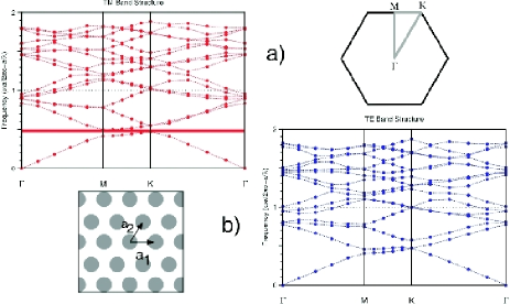
Numerical studies are carried out using three commercial software from RSoft. In a first step a study of infinite PhCs is performed by a PWE (Plane Wave Expansion) software (RSoft ) to find the PBG and to optimize the parameters of the nanostructure (hole size and period). In a second step electromagnetic field propagation in the nanostructures is numerically mapped by a FDTD calculation (RSoft ). Rigorous analysis of geometrical parameters like hole depth or surface roughness requires 3D calculation, which demands too many computer ressource. Therefore, we shall limit our study to 2D calculation applied to a 2D equivalent structure, to describe the general behavior of the 3D structure. The basic structure studied is a triangular lattice of holes centered on the waveguide as shown in Fig.1a. The equivalent 2D structure we chose is a vertical guiding slab with a lattice of infinite vertical holes centered inside.
The free waveguide properties (modes, propagation, losses…) are obtained by a BPM (Beam Propagation Method) software (RSoft ).
II.1 Photonic bandgaps calculation
For the wavelength , effective index of the multilayer waveguide is calculated by the BPM software to be . Our calculation gives complete photonic band gap in the case of triangular lattice for only one polarization (TM) (Fig.2), for a hole diameter between , and ( is the period of the lattice). Figure 2 shows the band diagram for . A TM PBG can be obtained for frequencies . The fact that the PBG in TM mode is very narrow and that there is no complete band gap in the other polarisation can be explained by the low index difference between the material and the holes ().
Afterwards we only consider holes of period and diameter . These values were chosen to fit with technological limitations (the ratio can hardly exceed 0.7 in the milling process) and to obtain a bandgap in the wavelength range (around 700-980nm) given by the tunable laser (See IV).
II.2 FDTD Simulations
After determining the parameters of the hole lattice the combination of the nanostructures with the waveguide can be characterized by FDTD calculation.
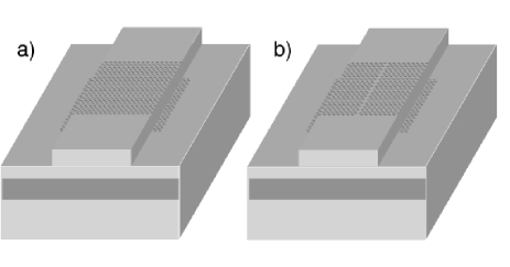
Two structures were modelled: the first one is a complete lattice, in the second one a line of holes has been removed at the center of the waveguide ( Fig.1b). It is expected that the lattice of holes without defects will behave like a mirror for wavelengths included in the photonic band gap.
II.2.1 Complete triangular lattice of holes
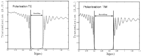
Light is injected in the equivalent planar waveguide wherein the hole lattice has been pierced according to the previous parameters. In a first step, transmission spectra have been calculated by injecting a pulse excitation in the direction . Two samples of this spectrum are presented in Fig.3. Although PBG calculation exhibits no complete band gap for TE polarisation and a narrow one for TM polarisation, the spectrum shows a band gap for both polarisations. For TE polarisation a fall of transmission efficiency can be noticed for wavelengths between et . In TM polarisation a similar PBG exists for wavelengths between and . It must be noticed that a partial band gap can exist for a given incidence, even if the crystal has no complete band gap (independent of the incidence). In the present case, the spectra of Fig. 3 correspond to the partial band gaps observed on the vertical line of Fig. 2. It can be verified that the width given by FDTD is slightly smaller () than the previous one as shown in table I. This discrepancy can probably be explained by the plane wave expansion of the guided mode : the direction of incidence is not limited to the waveguide axis .
| BandSolve | FullWave | |
| TE | 0.0495 | 0.0391 |
|---|---|---|
| TM | 0.0795 | 0.0621 |
| TM complete PBG |
The fall of transmission increases with the number of periods in the propagation direction. We found that a minimum of ten periods is necessary to obtain a transmission. For this example, 40 periods have been used.
Then, by launching continuous excitation and waiting for field stabilization in the structure, a mapping of each field (, and for TE polarisation, , and for TM polarisation) can be obtained as shown in Fig.4. For , light can pass through the lattice, but for , light seems to be completely reflected.
II.2.2 Triangular lattice with a line defect
We carried out the same calculation for a triangular lattice of holes where one line is missing. Light propagation is always in the direction . Transmission spectrum shows that the band gap has been perturbed and that some peaks appear (See Fig.5(a)). For a better coupling efficiency between optical waveguide and PBG waveguide of different width, a taper would be desirable (optical waveguide is wide and a line missing line is wide of one period of the lattice ()). Nevertheless 2D FDTD calculation at the wavelength corresponding to the higher peak () exhibits a high confinement of light in the line defect (See Fig.5 (b)). A calculation made at PBG wavelengths shows no light propagation in this line defect: the result is similar to Fig.4 (b).
III NANOSTRUCTURING OPTICAL WAVEGUIDES
Photonic crystal fabrication remains a challenge mainly due to the size and the depth of engraved holes. In our case, hole diameter is and the depth has to be more than to overlap the optical guided mode. Moreover, as optical waveguides have been fabricated beforehand, a good precision is needed to align correctly waveguides and nanostructures.
In a previous work lacour04 , we have demonstrated the possibility of nanostructuring lithium niobate substrate by Focused Ion Beam (FIB) the dimension of which is less than . Other laboratories have obtained FIB patterns at submicrometer scale gierak01 with good optical properties Dale00 ; bostan03 . Furthermore the main advantage of FIB is the ability to drill holes directly from the sample surface and the direct control of the structures after milling.
III.1 Waveguide fabrication
Optical waveguides are an important part in the fabrication of the sample since they guide light to nanostructures and also provide optical confinement in the third dimension.
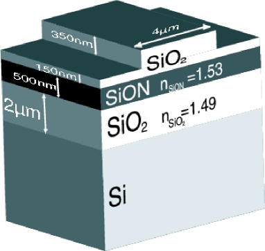
The optical waveguides (Fig.6) we have chosen are multilayer waveguides () deposited on a substrate. The three layers (, thickness: , : and again: ) are deposited by PECVD process. This process allows a good control over the thickness and over the optical index of the different layers. After a lithographic masking the rib waveguides are etched by RIE process on the top layer.
For the chosen parameters, BPM calculation have shown that waveguides are single mode over the wavelength scale which will be used for near-field characterization ().
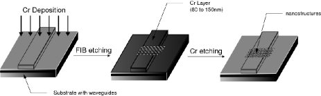
III.2 Nanostructuring waveguides with FIB
The fabrication process (See Fig.7) is based on a direct etching of the sample substrate by FIB bombardement. The samples, on which multilayer waveguides have been previously fabricated, are chromium coated ( layer) by electron gun evaporation to avoid charging, and grounded with a conductive paste before introduction in the FIB vacuum chamber (). Then the sample is milled using a FIB column (Orsay-Physics - LEO FIB4400). ion are emitted with a current of and accelerated by a voltage of . The probe current of the focused beam is or . The Gaussian-shaped spot size is estimated to be in the best conditions. The ion beam scans the sample, the deflection field being controlled by a software to produce the desired pattern.
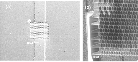
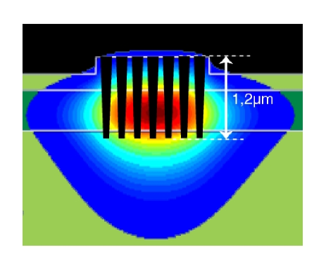
Several triangular lattice of circular holes with previously determined parameters ( and ) have been milled on the substrate. Fig.8 shows two views of a hole lattice fabricated by FIB. The cross section realized by FIB (Fig.8 (b)) provides important information about the hole depth (which we expect to be more than deep), the surface aspect and the hole shape . Hole shape is not cylindrical as we first wanted but conical. The upper diameter at the surface is about and the bottom diameter . This kind of problem is a fundamental drawback of FIB milling due to material redeposition during the scanning process. More vertical sidewalls can be obtained by using reactive gases during the FIB process.
IV Characterization
We have characterized this fabricated nanostructures using two different methods. A transmission spectrum of those nanostructures has first been studied by measuring the ratio between intensities of injected light and recovered light at the waveguide extremity. The second method is an in-situ characterization of the nanostructures with a stand-alone near-field microscope working in detection mode. This technique has been employed by several laboratories, more specifically in the study of high electromagnetic confinement (See peeters00 ; Colas01 ; Bolzhevolnyi02 ; Gerard02 ; Kramper04 ).
IV.1 Transmission spectrum
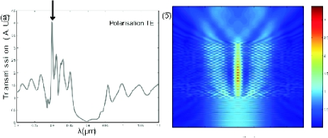
A tunable Titane-Sapphire Laser is used to scan a wavelength range from to . Its beam is injected into a polarization maintaining optical fiber which can be oriented to select TE or TM polarization. Light is injected directly in the optical waveguides from this fiber to limit the optical losses. Injection is controlled by collecting the guided mode from the end face of the waveguide by a microscope objective and a CCD camera (Fig.10). The transmission spectrum exhibits variations of about but does not show any clear photonic band gap.
The reason seems to be the out-of-plane losses caused by the perforation of the waveguide which induces a coupling of the guided wave with radiation modes. Recent work benisty02 ; ferrini03 ; ferrini03b has demonstrated that out-of-plane losses in planar PhCs depend on two principal parameters: they occur when the overlap between the guided mode and the nanostructures is not complete and when the sidewalls of holes are not vertical. From the cross-section of Fig.8 (b) the tilt of the sidewall is about and the holes are deeper than the core layer but do not overlap the mode completely. Fig.9 superimposes the hole profile and the BPM calculated optical mode. Reference ferrini03 demonstrates that a sidewall tilt bigger than may have disastrous consequences on the effect.
Even if a real PBG cannot be observed by transmission spectrum, we’ll see that near-field characterization could show relevant information on these nanostructures.
IV.2 Near-field characterization
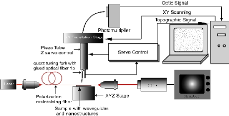
IV.2.1 Experimental setup
A stand-alone microscope has been used to characterize nanostructures on waveguides (Fig.10). The evanescent wave on top of the structure is collected by an optical probe made of an optical fiber tapered by the pulling/heating method under laser beam. Gluing the probe to a tuning fork ensures the usual distance control by shear-force feedback. The laser beam is modulated by a chopper and the optical signal measured by synchronous detection. Both topographic signal from feedback control and optical signal are recorded by a computer, which controls the XY scanning.
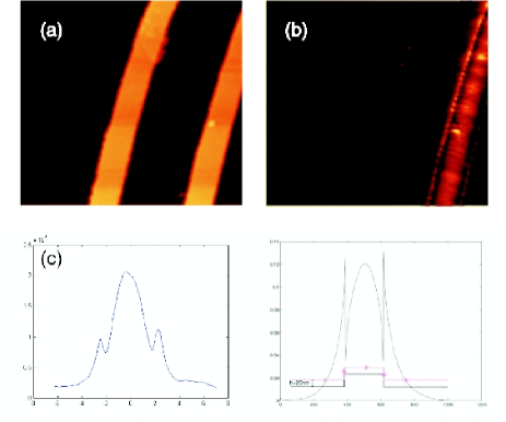
IV.2.2 Near-field characterization of bare waveguides
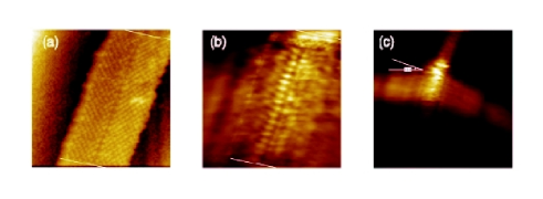
Imaging the bare waveguides was a means to test the near-field microscope on a well known intensity distribution and to control the guiding quality of the fabricated waveguides. Fig.11 (a) and (b) show respectively topographic and optical image of two waveguides. Light has been injected only into the right waveguide. Optical image shows that no light has been collected into the second waveguide despite the fact that the two waveguides were apart. The optical image (Fig.11 (b)) and its section (Fig.11 (c)) show a minimum of intensity at the edges of waveguide, which matches with the theorical optical field intensity section calculated at constant distance by BPM calculation (Fig. 11 (e)).
IV.2.3 Near-field characterization of a complete lattice
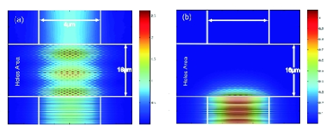
We have characterized at different wavelengths a lattice of holes (diameter: , period: ) pierced on the waveguide. Even if transmission spectra did not show any clear photonic band , light penetration into such structures have important variations with the wavelength. Two images (topographic and optical) at two wavelengths (Fig.12), one in the theorical band gap (, Fig.12 (c)), the other out of the bandgap (, Fig.12 (b)) show two completely different behaviours. Topographic image (Fig.12 (a) and (c)) exhibits periodic nanostructures (between white lines). Light propagates from top to bottom. Fig.12 (b) shows a deep penetration of the light into the structure. For the other wavelength, Fig.12 (c) shows a bright zone near the upper limit of the hole lattice but light decreases rapidly inside the lattice. The transmission efficiency (ratio output/input) of the lattice is five times greater at than at .
Fringes inside and in front of the lattice must be noticed: multiple reflections inside such structures and standing waves outside could explain this phenomenon.
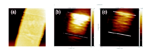
IV.2.4 Near-field characterization of a lattice with a line defect
A second type of structure ( hole lattice with a line missing in its center) has been characterized. It can be considered as a photonic waveguide, in which the injection would require a taper to ensure an efficient connection to the conventional waveguide, as its width is 10 times smaller.
As in the previous part, penetration and propagation of light into the structure depends on the wavelength. Fig.13 shows topographic and optical images at which is outside the theoretical bandgap. On the topographic image the missing line is visible in the center of the waveguide. The optical signal exhibits a dark line located on the missing holes and two lines of bright dots on both sides. This result presents similarities with the numerical simulation Fig.5 (b). These bright lines are completed by two diffracted beam which are guided in the SiON layer on both sides of the waveguide (Fig.13(c)).
V CONCLUSIONS
Direct FIB milling has shown some limits (hole shape, etching depth) which have caused imperfection in the fabricated photonic crystals. We are improving another similar way of fabricating such nanostructures: FIB is used only to engrave a thick metallic layer, which is considered as a mask for RIE or deep-RIE. A shorter milling time and a better aspect ratio are expected from this process.
In the present conditions the 2D approximation we used in FDTD simulation helped us to chose the wavelength domain in the characterization but the imperfect structures had no bandgap effect to be compared with the theoretical one. In spite of this difficulty the characterization of imperfect photonic structures is an example of the diagnosis delivered by near-field probing applied to complex 3D structures, the properties of which are not predicted by a 2D model. Despite the imperfection of the fabricated structures, the experimental and theoretical images of light propagation in a line-defect lattice present interesting similarities.
Acknowledgements.
Many thanks to Éloïse Devaux (INIST, Strasbourg) for her technical assistance and to Maria-Pilar Bernal, Matthieu Roussey, Nadège Bodin, Dominique Heinis for fruitful discussions.References
- (1) J. D. Joannopoulos and R. D. Meale and J. N. Winn, ”Photonic Crystals, Molding the Flow of Light”, princeton University Press (1995).
- (2) E. Chow, S. Y. Lin, S.G. Johnson, P. R. Villeneuve, J. D. Joannopoulos, J. R. Wendt, G. A. Vawter, W. Zubrzycki, H. Hou and A. Alleman, Nature 407, 983 (2000).
- (3) M. Józwik, C. Gorecki, A. Sabac, P. Delobelle and M. Kujawińska, Optics and Lasers Engineering, 41, 703 (2004).
- (4) F. Lacour, N. Courjal, M.-P. Bernal, A. Sabac, C. Bainier and M. Spajer, Opt. Mater. 27, 1421 (2005).
- (5) G. Dale, R.M. Langford, P.J.S. Ewen and C.M. Reeves,J. Non-crystalline Solids, 266, 913 (2000).
- (6) J. Gierak, D. Mailly, G. Faini, J.L. Pelouard, P. Denk, F. Pardo, J.Y. Marzin, A. Septier, G. Schmid, J. Ferr , R. Hydman, C. Chappert, J. Flicstein, B. Gayral and J.M. G rard, Microelect. Eng., 57, 865 (2001).
- (7) C. G. Bostan, R. M. de Ridder, V. J. Gadgil, L. Kuipers and A. Driessen, Proceedings Symposium IEEE/LEOS (Benelux chapter, Enschede, 2003), p.253.
- (8) R. Ferrini, B. Lombardet, B. Wild, R. Houdré and G. H. Duan, App. Phys. Lett. 82, 1009 (2003).
- (9) H. Bénisty, Ph. Lalanne, S. Olivier, M. Rattier, C. Weisbuch, C.J.M. Smith, T.F. Krauss, C. Jouanin and D. Cassagne, Opt. Quant. Electr. 34, 205 (2002).
- (10) R. Ferrini, R. Houdré, H. Benisty, M. Qiu, J Moosburger, J. Opt. Soc. Am. B 20, 469 (2003).
- (11) C. Peeters, E. Flück, A.M. Otter, M.L.M. Balistreri, J.P. Korterik, L. Kuipers and N.F. van Hulst, Appl. Phys. Lett. 77, 142 (2000).
- (12) D. Mulin, C. Girard, G. Colas des Francs, M. Spajer and D. Courjon, Journal of Microscopy 202, 110 (2001).
- (13) S.I. Bolzhevolnyi, V.S. Volkov, J.Arentoft, A. Boltasseva, T. Søndergaard and M. Kristensen, Opt. Comm. 212, 51 (2002).
- (14) D. Gérard, L. Berguiga, F. de Fornel, L. Salomon, C. Seassal, X. Letartre, P. Rojo-Romeo and P. Viktorovitch, Opt. Lett. 27, 173 (2002).
- (15) P. Kramper, M. Kafesaki, C.M. Soukoulis. A. Birner, F. Müller, U. Gösele, R.B. Whehrspohn, J. Mlynek and V. Sandoghdar, Opt. Lett. 29, 174 (2004).