Present address: ]Department of Physics, University of Ioannina, Ioannina 45 110, Greece
Scanning Gate Microscopy of a Nanostructure where Electrons Interact
Abstract
We show that scanning gate microscopy can be used for probing electron-electron interactions inside a nanostructure. We assume a simple model made of two non interacting strips attached to an interacting nanosystem. In one of the strips, the electrostatic potential can be locally varied by a charged tip. This change induces corrections upon the nanosystem Hartree-Fock self-energies which enhance the fringes spaced by half the Fermi wave length in the images giving the quantum conductance as a function of the tip position.
pacs:
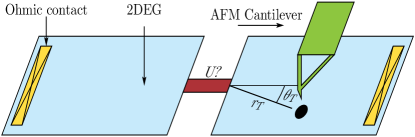
07.79.-v,71.10.-w,72.10.-d,73.23.-bSemiconductor nanostructures based on two dimensional electron gases (2DEGs) have been extensively studied, with the expectation of developing future devices for sensing, information processing and quantum computation. Scanning gate microscopy (SGM) consists in using the charged tip of an AFM cantilever as a movable gate for studying these nanostructures. A typical SGM setup is sketched in FIG. 1. A negatively charged tip capacitively couples with the 2DEG at a distance from the nanostructure, creating a small depletion region that scatters the electrons. Scanning the tip around the nanostructure and measuring the quantum conductance between two ohmic contacts put on each side of the nanostructure as a function of the tip position provide the SGM images. If the nanostructure is a quantum point contact (QPC), the charged tip can reduce Topinka et al. (2001) by a significant fraction , when the conductance without tip is biased on the first conductance plateau . Moreover, fringes spaced by , half the Fermi wave length, and falling off with distance from the QPC, can be seen in the experimental images giving as a function of the tip position. Very small distances were not scanned in Refs. Topinka et al. (2000, 2001), but this was done Aoki et al. (2006) later, giving extra ring structures inside the QPC if is biased between the conductance plateaus. Scanning gate microscopy has been recently used for studying QPCs Jura et al. (2007), open quantum rings Martins et al. (2007) and quantum dots created in carbon nanotubes Woodside and McEuen (2002) and 2DEGs Pioda et al. (2004).
Many features of the observed SGM images can be described by single particle theories Heller et al. (2005); Metalidis and Bruno (2005); Martins et al. (2007). However, many body effects are expected to be important inside certain nanostructures (almost closed QPC around the conductance anomaly Thomas et al. (1996), quantum dots of low electron density). We show in this letter that these many body effects can be observed in the SGM images of such nanostructures. Two main signatures of the interaction are identified: fringes of enhanced magnitude, falling off as near the nanostructure, before falling off as far from the nanostructure, and a phase shift of the fringes between these two regions. Though we study this interaction effect using a very simple model, our theory can be extended to any nanostructure inside which electrons interact.
Without interaction, the nanostructure and the depletion region created by the tip are independent scatterers. With interactions inside the nanostructure, the effective nanostructure transmission becomes non local and can be modified by the tip. The origin of this non local effect is easy to explain Asada et al. (2006); Freyn and Pichard (2007a, b) if one uses the Hartree-Fock (HF) approximation. The tip induces Friedel oscillations of the electron density, which can modify the density inside the nanostructure. As one moves the tip, this changes the Hartree corrections of the nanostructure. A similar effect changes also the Fock corrections Asada et al. (2006); Freyn and Pichard (2007a, b). When the electrons do not interact inside the nanostructure, the SGM images probe the interferences of electrons which are transmitted by the nanostructure and elastically backscattered by the tip at the Fermi energy . When the electrons interact inside the nanostructure, the information given by the SGM images becomes more complex, since the scattering processes of energies below influence also the quantum conductance. In the HF approximation, these non local processes taking place at all energies below are taken into account by the integral equations giving the nanosystem HF corrections.
The principle for the detection of the interaction via SGM can be simply explained in one dimension, when the strips are semi-infinite chains. If , the transmitted flow interferes with the flow reflected by the tip, giving rise to Fabry-Pérot oscillations which do not decay as . Hence the conductance of a nanostructure in series with a tip exhibits oscillations which do not decay when increases. If , the HF-corrections of the nanostructure are modified by the Friedel oscillations induced by the tip inside the nanostructure. This gives an additional effect for , which decays as the Friedel oscillations causing it (-decay in 1d, with oscillations of period ). Measuring as a function of the tip position, one gets oscillations of period in the two cases, but their decays are different and allow to measure the interaction strength inside the nanosystem.
Interactions in 1d chains give rise to a Luttinger-Tomonaga liquid and cannot be neglected. It is necessary to take 2d strips of sufficient electron density (small factor ) for neglecting interaction outside the nanosystem. The effect of the tip becomes more subtle with 2d strips: First, the Friedel oscillations decreasing as in dimensions, the effect of the tip upon has a faster decay, unless focusing effects take place. Second, the non interacting limit becomes more complicated. The probability for an electron of energy to reach the tip, and to be reflected through the nanostructure also decays as . Assuming isotropy, the probabilities of these two events should decay as , giving a total decay for . But isotropy is not a realistic assumption for SGM setups. The transmission can be strongly focused, making the effect of the tip a function of the angle . Spectacular focusing effects have been observed Topinka et al. (2000) using a QPC: The effect of the tip is mainly focused around or , depending if or .
For studying SGM with 2d strips more precisely, we use a simple model sketched in FIG. 2 (left), assuming spin polarized electrons (spinless fermions). The Hamiltonian reads . For the nanostructure, we take a nanosystem with two sites of energy and of hopping term . For the interaction, we take a repulsion of strength between these two sites. We assume that can be varied by an external gate. The Hamiltonian of the nanosystem reads
| (1) |
() is the annihilation (creation) operator at site , and .
| (2) |
describes the strips and their couplings to the nanosystem (see FIG. 2 (left)). We assume hard wall boundaries in the -direction. sets the energy scale. The depletion (accumulation) region created by a negatively (positively) charged tip located on top of a site of coordinates is described by a local Hamiltonian .
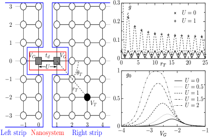
In FIG. 2 (upper right), we show how to detect by scanning gate microscopy in the 1d limit of our model (). The chains are half-filled (), and the conductance of the nanosystem in series with a tip is given as a function of . If , exhibits even-odd oscillations of constant amplitude, while these oscillations fall off as near the nanosystem if . When , the HF corrections can be obtained using an extrapolation method Asada et al. (2006); Freyn and Pichard (2007a, b). When is large, using self-energies becomes more efficient for calculating the HF corrections and the conductance .
The retarded () and advanced () Green’s functions of the nanosystem at an energy , are given by the -matrix
| (3) |
The self-energies and describe the couplings of the left and right strips to the nanosystem sites and respectively. If are the Green’s functions of the two strips excluding the 2 nanosystem sites, one gets
| (4) | |||||
| (5) |
and label the sites and directly coupled to for , and the sites and directly coupled to for . For each tip position and different energies , the Green’s functions of the right strip determining are calculated using recursive Green’s function (RGF) algorithm (see Ref. Metalidis and Bruno (2005) and references therein).
The self-energies and describe the Hartree corrections yielded by the inter-site repulsion to the potentials of the sites and respectively, while the Fock self-energy modifies the hopping term because of exchange. The matrix elements () being given by Eq. (3), the HF self-energies are the self-consistent solution of 3 coupled integral equations:
| (6) | |||||
| (7) | |||||
| (8) |
The imaginary parts of the above integrals are equal to zero for . For , the poles on the real axis make necessary to integrate Eqs. (6-8) using Cauchy theorem. We have used a semi-circle centered at in the upper part of the complex plane. The integration is done using the Gauss–Kronrod algorithm. This requires to calculate (and therefore and ) for a sufficient number () of complex energies on the semi-circle, before determining the self-consistent solutions of Eqs. (6- 8) recursively. Calculating for each tip position (), one can obtain the 2d images giving as a function of the tip position.
Once the self-energies are obtained in the zero temperature limit, the interacting nanosystem is described by an effective one body Green’s function, identical to the one of a non interacting nanosystem, with potentials and and hopping . Then, the many channel Landauer-Buttiker formula valid for non interacting systems can be used to obtain the zero temperature conductance in units of (for polarized electrons). This conductance corresponds to a measure made between the two ohmic contacts sketched in FIG. 1. We use the RGF algorithm to obtain the Green’s function of the measured system, from which the transmission matrix can be expressed Datta (1997).
For having negligible lattice effects and SGM images characteristic of the continuum limit, we consider a low filling factor in the 2d strips, corresponding to a Fermi energy (momentum) (). The width of the strip () is sufficient for having a 2d behavior in the vicinity of the nanosystem. Moreover, we take small values of the nanosystem hopping , in order to increase Freyn and Pichard (2007a, b) the effect of the tip upon the HF self-energies. In FIG. 2 (lower right), the conductance without tip () is given as a function of the gate potential for increasing values of . When is small, the double peak structure of characteristic of a nanosystem with two sites merges Freyn and Pichard (2007b) to form a single peak. Hereafter, the SGM images are given for a gate potential for which is maximum.
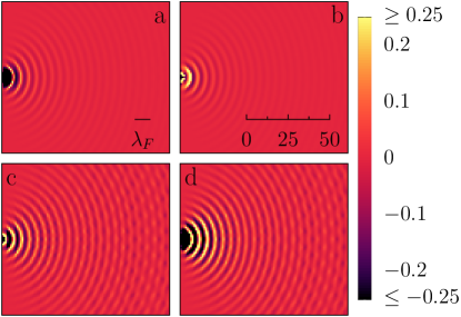

The effect of the tip upon and is shown as a function of the tip position () in the upper part of FIG. 3. The images show fringes spaced by which fall off as . In FIG. 4 (upper left), the Fock term is plotted as a function of for . The decay can be described by a fit. Similar fits characterize the 2 Hartree terms. Since the effect of the tip upon is driven by Friedel oscillations, decays as 2d Friedel oscillations. and have similar decays.
In the lower part of FIG. 3, the effect of the tip upon the conductance is given as a function of (). The left figure gives without interaction (), where . One can see that decays as increases, the image exhibiting fringes spaced by . The decay depends on the angle . For , falls off as , and not as (isotropic assumption). This is shown in FIG. 4 (upper right), a fit of the form describing the decay.
In FIG. 3 (d), is shown when the electrons interact inside the nanosystem (). The interation effect of the tip upon via enhances the fringes near the nanosystem. Since the SGM images exhibit fringes spaced by , decaying as for and as for when , we fit the effect of the tip upon when by a function
| (9) |
which contains 4 adjustable parameters and . The terms give the fringes. The term fits the decay without interaction. The term is added for taking into account the effect of the tip upon occurring near the nanosystem via .
When is large, the effect of the tip upon is negligible and falls off as when ( decay). As varies, a crossover from a decay described by the term of towards a decay described by takes place. This is shown in FIG. 4 (lower part), where is necessary for describing at small distances . This crossover is accompanied by a phase shift of the fringes (), which can be seen in the figure. To find this crossover, we have studied how the 4 parameters of depend on and on (insets of FIG. 4). To get a decay which persists in a large domain around the nanosystem, one needs . This occurs for small (upper inset) and (lower inset).
In summary, neglecting electron-electron interactions and disorder in the strips, we have shown that the SGM images allow to measure the interaction strength inside the nanosystem. From zero temperature transport measurements, one can detect a decay of the SGM images around the nanosystem, and via , the value of characteristic of the nanosystem can be determined. For observing this decay, one needs (i) large electron-electron interactions inside the nanostructure (sufficient factor), (ii) large density oscillations induced by the tip ( large), and (iii) that those oscillations modify the density inside the nanostructure ( not too large, strong coupling between the nanostructure and the strips).
Acknowledgements.
We thank S. N. Evangelou for useful comments and a careful reading of the manuscript. The support of the network “Fundamentals of nanoelectronics” of the EU (contract MCRTN-CT-2003-504574) is gratefully acknowledged.References
- Topinka et al. (2001) M. A. Topinka, B. J. LeRoy, R. M. Westervelt, S. E. J. Shaw, R. Fleischmann, E. J. Heller, K. D. Maranowski, and A. C. Gossard, Nature 410, 183 (2001).
- Topinka et al. (2000) M. A. Topinka, B. J. LeRoy, S. E. J. Shaw, E. J. Heller, R. M. Westervelt, K. D. Maranowski, and A. C. Gossard, Science 289, 2323 (2000).
- Aoki et al. (2006) N. Aoki, A. Burke, C. R. da Cunha, R. Akis, D. K. Ferry, and Y. Ochiai, J. Phys.: Conf. Series 38, 79 (2006).
- Jura et al. (2007) M. P. Jura, M. A. Topinka, L. Urban, A. Yazdani, H. Shtrikman, L. N. Pfeiffer, K. W. West, and D. Goldhaber-Gordon, Nature 3, 841 (2007).
- Martins et al. (2007) F. Martins, B. Hackens, M. G. Pala, T. Ouisse, H. Sellier, X. Wallart, S. Bollaert, A. Cappy, J. Chevrier, V. Bayot, et al., Phys. Rev. Lett. 99, 136807 (2007).
- Woodside and McEuen (2002) M. T. Woodside and P. L. McEuen, Science 296, 1098 (2002).
- Pioda et al. (2004) A. Pioda, S. Kicin, T. Ihn, M. Sigrist, A. Fuhrer, K. Ensslin, A. Weichselbaum, S. E. Ulloa, M. Reinwald, and W. Wegscheider, Phys. Rev. Lett. 93, 216801 (2004).
- Heller et al. (2005) E. J. Heller, K. E. Aidala, B. J. LeRoy, A. C. Bleszynski, A. Kalben, R. M. Westervelt, K. D. Maranowski, and A. C. Gossard, Nano Lett. 5, 1285 (2005).
- Metalidis and Bruno (2005) G. Metalidis and P. Bruno, Phys. Rev. B 72, 235304 (2005).
- Thomas et al. (1996) K. J. Thomas, J. T. Nicholls, M. Y. Simmons, M. Pepper, D. R. Mace, and D. A. Ritchie, Phys. Rev. Lett. 77, 135 (1996).
- Asada et al. (2006) Y. Asada, A. Freyn, and J.-L. Pichard, Eur. Phys. J. B 53, 109 (2006).
- Freyn and Pichard (2007a) A. Freyn and J.-L. Pichard, Phys. Rev. Lett. 98, 186401 (2007a).
- Freyn and Pichard (2007b) A. Freyn and J.-L. Pichard, Eur. Phys. J. B 58, 279 (2007b).
- Datta (1997) S. Datta, Electronic Transport in Mesoscopic Systems (Cambridge University Press, 1997).