Silicon Vertex Tracker for PHENIX Upgrade at RHIC: Capabilities and Detector Technology
Abstract:
From the wealth of data obtained from the first three years of RHIC operation, the four RHIC experiments, BRAHMS, PHENIX, PHOBOS and STAR, have concluded that a high density partonic matter is formed at central Au+Au collisions at . The research focus now shifts from initial discovery to a detailed exploration of partonic matter. Particles carrying heavy flavor, i.e. charm or beauty quarks, are powerful tool for study the properties of the hot and dense medium created in high-energy nuclear collisions at RHIC. At the relatively low transverse momentum region, the collective motion of the heavy flavor will be a sensitive signal for the thermalization of light flavors. They also allow to probe the spin structure of the proton in a new and precise way. An upgrade of RHIC (RHIC-II) is intended for the second half of the decade, with a luminosity increase to about 20-40 times the design value of 8 1026 cm-2 s-1 for Au+Au, and 2 1032 cm-2 s-1 for polarized proton beams. The PHENIX collaboration plans to upgrade its experiment to exploit with an enhanced detector new physics then in reach. For this purpose, we are constructing the Silicon Vertex Tracker (VTX). The VTX detector will provide us the tool to measure new physics observables that are not accessible at the present RHIC or available only with very limited accuracy. These include a precise determination of the charm production cross section, transverse momentum spectra at high- region for particles carrying beauty quarks as well the detection of recoil jets in direct photon production. The VTX detector consists of four layers of barrel detectors located in the region of pseudorapidity 1.2 and covers almost 2 azimuthal angle. The pseudorapidity, , is defined as , where is the emission angle relative to the beam axis. The inner two silicon barrels consists of silicon pixel sensors and their technology is the ALICE1LHCb sensor-readout hybrid, which was developed at CERN for the ALICE and LHCb experiments. The outer two barrels consists of silicon stripixel detector with a new ”spiral” design, single-sided sensor with 2-dimensional (X-U) read-out. In this paper, we will provide details of the physics capability added to PHENIX by the new central silicon vertex tracker, the status of the project, including technology choices used in the design, performance of individual silicon sensor and silicon detector prototype.
![[Uncaptioned image]](/html/0801.2947/assets/x2.png)
|
![[Uncaptioned image]](/html/0801.2947/assets/x3.png)
|
1 Physics Motivations and Goals
Particles carrying heavy flavor, i.e. charm or beauty quarks, are a powerful tool for study the properties of the hot and dense medium created in high-energy nuclear collisions like at RHIC. At the relatively low transverse momentum region, the collective motion of the heavy flavor will be a sensitive signal for the thermalization of light flavors at RHIC-II (RHIC-II is the upgrade of the RHIC). They allow the probing of the spin structure of the proton in a new and precise way.
The current PHENIX experiment at Relativistic Heavy Ion Collider (RHIC) at Brookhaven National Laboratory (BNL) is inadequately equipped to fully exploit the opportunities of heavy-flavor production provides. Many of the necessary measurements are either not possible or can be performed only with very limited accuracy. Precise vertex tracking is imperative for robust measurement of heavy-flavor production. The silicon vertex tracker (covering 1.2) which is under construction adds tracking capabilities to the two central arms (each central arm covers pseudorapidity region 0.35 and is composed of the drift chambers, pixel-pad chambers, and time expansion chambers) of the PHENIX experiment. With this detector, the charged particles detected in the central arms can be identified as decay products from charm or beauty carrying particles by measuring the distance of closest approach (DCA) to the primary vertex in such events.
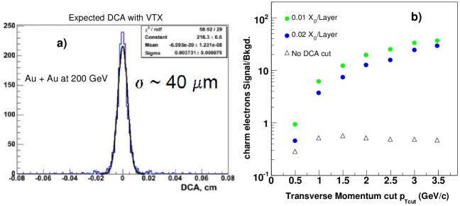
For heavy ion collisions or spin structure of the nucleon programs, we plan to observe charm and beauty production through its semi-leptonic decay to . We will need a good vertex resolution to identify the DCA to the primary vertex in such events. The main background expected for this physics include Dalitz decays and photon conversions have been studied using a GEANT detector simulation. We estimated that the VTX detector could achieve 40 DCA resolution as shown in figure 1.a. Using a DCA cut value of 200 for tracks with 1 GeV/c, we should be able to achieve a significant background reduction. As a result of the DCA cut, the purity of the event sample increases from 50% to 90% as presented by the simulation in figure 1.b.
Some of physics topics addressed by the PHENIX experiment upgraded by VTX detector in heavy ion collisions and spin structure of the nucleon are [1, 2]:
1.1 Heavy Ion Collisions:
The aim of ultra-relativistic heavy ion collisions is to produce and reveal a new phase of matter. When ions collide at very high velocity fascinating things happen. The RHIC is the first machine in the world capable of colliding heavy ions at nearly speeds of light (what Einstein called relativistic speeds). Recently, RHIC has discovered a new state of matter strongly interacting and more like a “perfect” liquid explained by the equations of hydrodynamics [3]. The evidence includes (1) bulk collective elliptic flow, (2) jet quenching and mono-jet production, observed in Au+Au central collisions at 200 GeV per nucleon, and (3) a critical control experiment using d+Au collisions at 200 GeV per nucleon. The research focus now shifts from initial discovery phase towards detailed investigation of the properties of the dense nuclear medium created in heavy ion collisions. The PHENIX experiment upgraded by VTX detectors [4] will allow to establish very precise measurements such as:
-
•
mass dependence of the energy-loss of partons in the medium expressed in figure 3.a by nuclear modification factor relative to + collisions, which has been observed for light partons, ()/2. Figure 3.a shows the expected results for charged particles ()/2 detected in the central arms identified as decay products from charm or beauty in PHENIX experiment by adding VTX detector.
-
•
mass dependence of elliptic flow of quarks. Figure 3.b presents the elliptic flow amplitude of electrons, ()/2, issued from heavy-flavor decays at midrapidity region in Au+Au collisions at . Figure 3.b presents the expected elliptic flow strength v2, of single electrons from heavy flavor decay measured in PHENIX experiment by adding VTX detector. A strong elliptic flow is evidence of strong coupling Quark-Gluon Plasma (sQGP).
-
•
a firm baseline to quantify the suppression or possible enhancement of
The present PHENIX can not distinguish single electrons from charm decay and from beauty decay in Au+Au collisions. Thus we can not determine the suppression factor, RAA (or elliptic flow, v2) of charm accurately, nor we can determine if beauty also suffer significant energy loss or not. The VTX detector will allow us to measure the single electrons from charm and beauty separately. Since beauty has a larger c (B0: 462 m, B+: 502 m) than charm (D0: 123 m, D+: 317 m), we can accurately split the beauty component of single electron from the charm component using a precise displaced vertex measurement from the VTX detector as shown in Fig. 3. The VTX detector will also allow us to measure the high-pT spectra of charm directly via the hadronic decay channels, e.g. D K . From these measurements, we will be able to determine the energy loss of charm and beauty in the medium. This will be a decisive measurement to understand the energy loss mechanism in the dense matter at RHIC.
1.2 Spin Structure of the Nucleon:
Spin plays a central role in our theory of the strong interaction, Quantum Chromodynamics or QCD. The PHENIX experiment with polarized protons colliding at RHIC probe the proton spin in new profound ways that are complementary to deep inelastic scattering experiments [5]. The proposed VTX detector will be crucial in the determination of gluon distribution in two significant ways:
-
•
different measurements will cover the same kinematic regions: this would enable the much-needed cross-checks within PHENIX for accessing the polarized gluon distribution. The VTX detector extends the reach in kinematic regions in (charm measurement and jet reconstruction over large acceptance of VTX detector significantly extend the -range, where is the Bjorken variable which describes the fraction of the nucleon momentum carried by a particular parton) for many of the measurements and hence adds a significant amount of overlap in -range coverage. Here ”coverage” implies we measure the ratio G/G (gluon spin polarization) with 20% relative uncertainty of its expected value at that x. For more details see Ref. [4].
-
•
by being able to observe displaced vertices at low- for semi-leptonic decays of charm and beauty, the VTX detector will enable a large -range over which we will make gluon polarization measurements. It is estimated that the reach of the VTX detector will be 0.01 0.3.
| Pixel Detector | Stripixel Detector | ||||
| VTX | Layer | R1 | R2 | R3 | R4 |
| Geometrical | R (cm) | 2.5 | 5 | 10 | 14 |
| dimensions | z (cm) | 21.5 | 21.8 | 31.8 | 38.2 |
| Area (cm2) | 280 | 560 | 1960 | 3400 | |
| Channel | Sensor size | 1.28 1.36 | 3.43 6.36 | ||
| count | R z(cm2) | (256 32 pixels) | (384 2 strips) | ||
| Channel | 50 425 m2 | 80 m 3 cm | |||
| size | (effective 80 1000 m2) | ||||
| Sensor/ladder | 4 4 | 5 | 5 | ||
| Ladders | 10 | 20 | 18 | 26 | |
| Sensors | 160 | 320 | 90 | 156 | |
| Readout chips | 160 | 320 | 1080 | 1872 | |
| Readout channels | 1,310,720 | 2,621,440 | 138,240 | 239,616 | |
| Radiation | Total | 1.44% | 2.1% | ||
| length (X/X0) | |||||
| Occupancy | Au+Au | 0.53% | 0.16% | 4.5% (xstrip) | 2.5% (xstrip) |
| at 200 GeV | 4.7% (ustrip) | 2.7% (ustrip) | |||
2 Overview of Silicon Vertex Tracker Detector
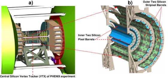
The central silicon vertex tracker (VTX) detector illustrated in figure 4 consists of four layers of barrel detectors, covers almost 2 azimuthal angle and pseudorapidity range 1.2. The inner two layers are built from silicon pixel sensors forming silicon pixel detector and the outer two layers are built from silicon stripixel sensors forming silicon stripixel detector. The summary of physical specifications of VTX are summarized in Table 1. The specifications have been chosen so that the design has a low material budget to avoid tracks being randomly bent by multiple scattering, and to minimize photon conversion ( ) which generates a background for electron identification in outer detectors. The VTX detector can be used in proton-proton collisions and the high multiplicity environment of heavy ion collisions.
![[Uncaptioned image]](/html/0801.2947/assets/x6.png)
|
![[Uncaptioned image]](/html/0801.2947/assets/x7.png)
|
2.1 Silicon Pixel Detector
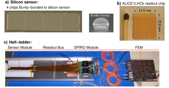
The two inner barrels of VTX detector consists of silicon pixel detectors (SPD) [4]. The technology of SPD is similar to the ALICE1LHCb sensor-readout hybrid, which was developed at CERN for the ALICE and LHCb experiment [6, 7]. The physical specifications of silicon pixel detector are summarized in Table 1. The first and second silicon pixel barrels consist of 10 and 20 ladders, respectively. One ladder is electrically divided into two independent half-ladders. Each ladder consists of four sensor modules mounted on a mechanical support (stave). Each sensor module consists of a silicon pixel sensor bump-bonded with four pixel readout chips. The readout chips (ALICE1LHCb) were developed by the CERN EP-MIC group and fabricated by using the IBM 0.25 m CMOS technology [8]. The library and the design techniques of the readout-chips guarantee the radiation hardness of the chip up to 30 kRads (for more details see Ref. [8]). The size of the chip is 15.6 mm 13.7 mm with 150 m thickness. One chip has 32 256 = 8,192 channels (pixels), each channel is pre-amplified and discriminated with a configurable threshold level. The discriminated binary signal is delayed with programmable duration, and then, stored to be read out by a downstream data acquisition system. The chip has 44 internal 8-bit Digital-to-Analog Converters for controlling the threshold of discriminators and various timings. All configurations are set via the JTAG serial interface (IEEE std. 1149.1-1990). The chip is operated using a 10 MHz clock. Therefore, the maximum readout speed is 25.6 sec with a 32-bit line. The sensor chip thickness is 200 m and its fabricated by CANBERRA. It is partitioned into four active areas. Each area has 32 columns (z) 256 rows () with a pixel size of 425 m (z) 50 m (). Pictures of silicon pixel module, pixel readout chip and the structure of half-ladder are presented in figure 5. a), b) and c), respectively.
The sensor modules of one half-ladder are wire-bonded to a readout bus made of Copper-Aluminum-Polyimide Flexible Printed Circuit board (FPC), which is supported by a carbon composite stave. This basic detector (half ladder) unit is read-out by a SPIRO module (SPIRO: Silicon Pixel Intermediate Read-Out). SPIRO modules are placed outside of the detector acceptance. They process the incoming control signals and transmit the outgoing data of a pixel half ladder. A SPIRO module carries analog Pilot chips for the power and reference voltage supplies of the pixel readout chips, digital Pilot chips for their controls and readout, and an optical link chips and transmitters for the data transfer. The SPIRO modules are then connected to pixel Front End Modules (FEMs) outside of the PHENIX IR. The FEMs work as interface to the PHENIX DAQ system. Since the SPIRO module transmits the data via optical fiber, the FEM can be located in electronic racks away from the vertex region. Each FEM may receive data from several pixel half ladders and thus reduce the number of Data Collection Modules (DCM) needed to interface to the PHENIX DAQ. In order to allow simple manipulations of the data, the FEM will pipe the data through an FPGA. This FPGA will add data headers and trailers to for standard PHENIX data packages. The design of the FEM is very similar to FEM’s that are currently employed in the PHENIX readout system. Additional information can be found in Ref. [9].
2.1.1 Performance of the silicon pixel detectors
To ensure long-term operation of silicon pixel detector, it is mandatory to study their performance. Recently, the functionality of the prototype silicon pixel detectors with pixel readout board (SPIRO) using PHENIX readout system was performed using cosmic-ray test [10]. The setup consists of a telescope made from three pixel layers (three half-ladders) connected to the PHENIX DAQ system. The trigger is made of a coincidence of self trigger signal (FastOR) on the layer-1, layer-2 and layer-3. Figure 7 shows typical cosmic-ray event observed by the three silicon pixel layers. Figure 7 shows the residual distributions on the -side and -side for tracks in the cosmic-ray sample.
The prototype silicon pixel detector was confirmed to be well functioning by finding tracks reconstructed by a telescope. The performance of the bus is measured and is compared with the simulation. The comparison with simulation indicates that the functionality of the pixel ladders satisfy the PHENIX requirements for the upgrade [4].
2.2 Silicon Stripixel Detector
The outer two barrels of the VTX detector for PHENIX experiment upgrade consists of silicon stripixel detector with a new ”spiral” design, single-sided sensor with 2-dimensional (X-U) readout [4].
2.2.1 Novel Stripixel Sensor Design and Specifications
A novel stripixel silicon sensor has been developed at BNL [11]. The silicon sensor is a single-sided, DC-coupled, two-dimensional (2D) sensitive detector. This design is simpler for sensor fabrication and signal processing than the conventional double-sided strip sensor. Each pixel from the stripixel sensor is made from two interleaved implants (a-pixel and b-pixel) in such a way that the charge deposited by ionizing particles can be seen by both implants as presented in figure 9.A. The a-pixels are connected to form a X-strip as is presented in figure 9.B. The b-pixels are connected in order to form a U-strip as is presented in figure 9.C. The stereo angle between a X-strip and a U-strip is 4.6o. A schematic cross section of the silicon stripixel sensor is presented in figure 9.a. The basic functionality of the sensor is simple; signal charges (electronhole pairs) generated for example by particles produced from collisions are separated by the electric field, the electrons moving to the n+ side, holes to the p+ side, thus producing an electric signal which can be amplified and detected. In figure 9.a, the first Al layer is the metal contacts for all pixels. All X-strips are routed out by the first metal Al layer. All U-strips are routed out by the second metal Al layer.
The size of the silicon stripixel sensor is about 3.43 6.36 cm2 and is shown in figure 9.b. In each long side of the sensor there are six sections of bonding pads, with 128 bonding pads each. This implies that each sensor has 2 3 128 = 768 of X-strips of 80 m width and 3.1 cm length in beam direction and the same number of U-strips at an angle of 4.6o to the beam direction. Due to the stereoscopic readout the effective pixel size is 80 1000 m. Five (for layer 3) or six (for layer 4) sensors are mounted in a ladder. The full length of a ladder in the beam direction is 31.8 cm (for layer 3) or 38.2 cm (for layer 4). A total of 44 ladders are required to cover the azimuth acceptance almost 2. The geometric characteristics of silicon stripixel layers are presented in Table 1. The novel stripixel silicon sensor technology developed, including the mask design and processing technology, has been transferred from BNL to sensor fabrication company Hamamatsu Photonics (HPK) located in Japan, for mass production. A picture of one sensor from full production is presented in figure 9.b.
![[Uncaptioned image]](/html/0801.2947/assets/x8.png)
|
![[Uncaptioned image]](/html/0801.2947/assets/x9.png)
|
![[Uncaptioned image]](/html/0801.2947/assets/x10.png)
|
![[Uncaptioned image]](/html/0801.2947/assets/x11.png)
|
To measure the total leakage current (Itot) of the sensor and eventually to extract the leakage current per strip (Istrip = Itot/Ntot where the total number of strips Ntot = 12 sections 128 strips = 1536 strips), two sensors that passed the quality assurance tests were mounted on two independent print circuit (PCBs) and wire bonded as shown in figure 11. The current and capacitance as a function of bias voltage were measured and normalized to 20 oC and they are presented in figure 11. We have studied the stability of the leakage current as function of time for a long period (22 days) and the temperature has been monitored for the same period. We observe that the leakage current is stable as a function of time and it has good correlation with the temperature of the clean-room [12]. In figure11, the measured total leakage current per stripixel can be obtained as Itot = 179 nA this implies Istrip = 179/1536 strips = 0.12 nA which is very low and it allows the use of the SVX4 chips, which have a hard limit of 15 nA/strip. This hard limit comes from that the leakage current from the DC-coupled sensor will rapidly saturate the SVX4 input preamp. The preamp dynamic range is 200 fC, which will saturate in 500 s with a 0.4 nA/strip. However, we can issue a preamp-reset signal once per RHIC abort ( 13 s). In fact, this reset frequency limitation puts a hard limit on the maximum acceptable leakage current. If the leakage current stays below this limit, we should not expect any problems due to leakage current [12].
2.2.2 Performance of Prototype Silicon Stripixel Module using ROC-V2
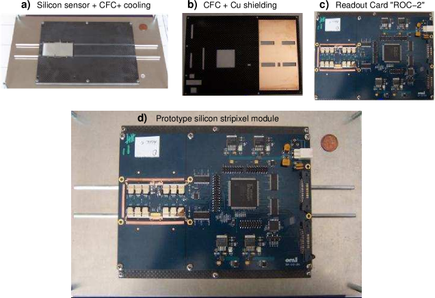
A prototype silicon stripixel module has been fabricated to evaluate performance of the stripixel sensor and Readout Card Version two (ROC-V2). As it is shown in figure 12.a), b) and c), the silicon stripixel module consists of one sensor thermal plate, one shielding layer and one Readout Card Version two (ROC-V2), respectively. The sensor thermal plate consists of one silicon sensor mounted on thermal plate made from Carbon Fiber composite (CFC) that contains two cooling tubes. The sensor thermal plate has also four spacers used to elevate the shielding layer and ROC-V2 from touching the sensor. The shielding layer consists of one CFC layer and one Copper layer (18 m thickness). The ROC-V2 is a thin printed circuit board (600 m) that hosts twelve SVX4s readout chips plus one field-programmable gate array (FPGA) required to digitize the data from one stripixel sensor and a few passive components.
The stripixel sensor is read out with the SVX4 chip developed by FNAL/Berkeley collaboration. The SVX4 chip is designed and fabricated in the 0.25 m CMOS process on 300 m thick silicon and has been successfully tested up to 10 Mrads. It contains 128 parallel charge integration channels and 8-bit ADCs. The chip is designed to run in a deadtime-less mode: the front-end (analog) part can run in parallel with the back-end (digital) part. For each channel, there are 46 pipeline cells to store the data. These can hold at most 4 events for further digitizing and readout. The operation voltage of the chip is 2.5 V. The other features of SVX4 chip are: 1) max interaction rate at 132 ns, 2) optimized capacitance load between 10 to 35 pF, 3) built-in charge injection for preamp calibration, 4) channel mask to exclude channels with excessive DC current input during operation, 5) readout in byte-serial mode with optional zero suppression (sparsification), 6) real-time event-by-event pedestal subtraction (RTPS) which can suppress the common mode noise and compensate for any residual pickup effects and 7) adjustable and loadable control parameters. The noise of a SVX4 chip is around 400 electrons. The dynamic range of the amplifier is 200 fC. The threshold and gain of the amplifier can be set to effectively readout a minimum ionizing particle (MIP) signal. Additional information on the SVX4 can be found in Ref. [13]. Prototyping efforts have allowed us to verify compatibility of the SVX4 with the PHENIX DAQ (serial programming, clock, fast control and data read-out). Command parsing and data formatting functions are implemented in FPGA and have been largely exercised with existing prototypes developed at ORNL (Oak Ridge National Laboratory). The data formatting code is particularly simple, and is almost entirely a subset of code developed for previous PHENIX subsystems. The interface between ROC-2 and the data acquisition (DAQ) is done by a Front-end Module (FEM) prototype. This communicates to a PC-computer via USB interface.
For the evaluation of the performance, the silicon stripixel module shown in figure 12.c was placed inside a dark-box and connected to the cooling system. The cooling system was running at 0 oC degree temperature. The cooling at 0 oC temperature is required when the detector will be operational under high radiation exposure (total fluence integrated over 10 years amounting up to 3.3 1012 n-eq/cm2) at RHIC-II and we have to keep the leakage current of the sensor below the saturation limit of SVX4, 15 nA/strip [12, 13]. The temperature and humidity inside the dark-box were monitored and were relatively stable as a function of time.
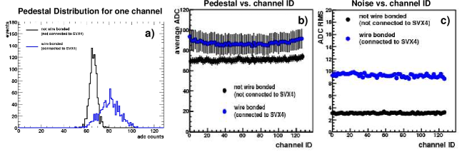
The primary goal of the evaluation of silicon stripixel module using ROC-V2 is to study the flatness of the pedestal and noise distributions as a function of stripixel number as well the stability of the distributions event-by-event. These informations are crucial for the use of the zero-suppression of SVX4 when it is connected to the silicon sensor and the configuration of the ROC-V2. The silicon stripixel module performances for the signal-to-noise and effects of irradiation dose on the silicon leakage current have been already done successfully by the first prototype silicon modules and can be found in Refs. [4, 12, 14]. The pedestal distribution for a given channel, pedestal and noise distributions versus channel number of silicon stripixel module are presented in figure 13.a , b and c, respectively. For the silicon stripixel module which used spacers to elevate the ROC-V2 from touching the silicon sensor, we did not succeed to do the full wire-bonding of all SVX4s to the silicon sensor (we had technical difficulties in wire-bonding the inner bonding pads of the silicon sensor to the SVX4s). However, by removing the spacers we succeeded to have one full wire-bonded silicon stripixel module (full wire-bonding of the twelve SVX4 to the silicon sensor). From test results, we observe that the noise per channel of wire-bonded channel of silicon stripixel module using ROC-V2 is around 9 ADC units and the noise distribution versus stripixel channel is flat. However, we observed that pedestal distribution of wire-bonded channels versus channel number are not completely flat. The test results of the silicon module using ROC-V2 suggest that there is charge sharing between the analog front ends of the SVX4 readout chips. Improved grounding by the inclusion of a solid, continuous, uniform analog-ground plane under the SVX4s and sensor, along with improved connections between the analog-ground and the sensor shield will reduce the amount of charge sharing.
3 Summary
The physics capabilities in heavy ion collisions and spin structure of the nucleon programs added to PHENIX by the new central silicon vertex tracker (VTX) upgrade have been presented. The technology choices used in the design, specifications, assembly procedures and data readout of prototype silicon modules of VTX, pixel and stripixel modules, have been elucidated. Cosmic-ray test results confirmed that prototype silicon pixel telescope (telescope made from three pixel layers) are performing well by finding tracks reconstructed. The performance of the pixel ladders was measured and the comparison with simulations indicates that the functionality of the pixel detector satisfy the PHENIX experiment requirements for the upgrade. The test results of the silicon module using ROC-V2 suggest that there is charge sharing between the analog front ends of the SVX4 readout chips. Improved grounding by the inclusion of a solid, continuous, uniform analog-ground plane under the SVX4s and sensor, along with improved connections between the analog-ground and the sensor shield will reduce the amount of charge sharing. The present status of the silicon stripixel module, we are in process of making new ROC-V3 which includes all informations obtained from silicon stripixel module using ROC-V2. We expect to have the first test results of the silicon stripixel module using the ROC-V3 readout card in first half of 2008.
Acknowledgments:
This manuscript has been authored by employees of Brookhaven Science
Associates, under Contract No. DE-AC02-98CH10886 with the
U.S. Department of Energy.
References
- [1] A. Adare, et al., Phys. Rev. Lett. 98, 172301 (2007).
- [2] K. Adcox, et al., Nucl. Inst. and Meth. A499, 469 (2003).
- [3] I. Arsene et al., Nucl. Phys. A 757, 1 (2005), K. Adcox et al. Nucl. Phys. A 757, 1 84 (2005) B. B. Back et al., Nucl. Phys. A 757, 28 (2005), and J. Adams et al., Nucl. Phys. A 757, 102 (2005.)
- [4] http://www.phenix.bnl.gov/phenix/WWW/p/docs/proposals/VTXPROPOSAL-jul2004.pdf
- [5] A. Airapetian et al. (HERMES collaboration), Phys. Rev. Lett. 94, 012002 (2005).
- [6] W. Snoeys, et al., Nucl. Inst. Meth. A466 (2001) 366.
- [7] K. Wyllie, ALICE1LHCB Document, CERN, 2003.
- [8] K. Wyllie, ALICE1LHCB Document, CERN, 2001.
- [9] E. J. Mannel et al., Proceeding of Real-Time Conference, 15th IEEE-NPSS 1 (2007).
- [10] M. Kurosawa, et al., RIKEN Accel. Prog. Rep. 41, 180 (2008).
- [11] Z. Li, Nucl. Instr. and Meth. A 518, 738 (2004).
- [12] R. Nouicer, et al., Nucl. Instr. and Meth. B 261, 1067 (2007).
- [13] http://www-cdf.lbl.gov/users/mweber/svx4/; another repository of information can be found in the FERMI NT domain located at d0server6.fnal.gov/projects/SVX4all-docs.
- [14] J. Tojo, et al., IEEE Trans. Nucl. Sci. NS-51 (5), 2337 (2004).