Indirect electric field doping of the CuO2 planes in NdBa2Cu3O7 cuprate
Abstract
The mechanism of field-effect doping in the “123” high critical temperature superconductors (HTS) has been investigated by x-ray absorption spectroscopy in the presence of an electric field. We demonstrate that holes are created at the CuO chains of the charge reservoir and that field-effect doping of the CuO2 planes occurs by charge transfer, from the chains to the planes, of a fraction of the overall induced holes. The electronic properties of the charge reservoir and of the dielectric/HTS interface determine the electric field doping of the CuO2 planes.
pacs:
74.78.-w, 74.25.Jb, 71.30.+hThe physical phenomena occurring at the interface between materials having different bulk electronic properties are extremely important in modern electronics REVMOD . The great success of the metal-oxide semiconductor field effect transistors is due to the high technological control of the Si/SiO2 interface and to the very good understanding of the electric field effect mechanisms at the interface between a band insulator and a band semiconductor. Such detailed insight is missing for the interfaces of materials with strong electron correlation, such as the high critical temperature superconductors (HTS).
The application of an electric field at the interface between an insulator and a metal/semiconductor is considered a general method to change reversibly the electronic properties of thin film without introducing chemical and structural disorder. In particular, the electric field-effect has been used to shift the critical temperature and even to induce phase transitions in conventional and high critical temperature superconductors FET1 ; FET2 ; FET3 ; FET4 ; FET5 ; FET6 . Experiments conducted on HTS from early 1990s to nowadays have been usually interpreted by supposing that the induced charges become carriers in the CuO2 conducting planes, thus changing the filling of the Zhang-Rice (ZR) band ZR . The universal relationship between and the carrier density in the CuO2 planes of the HTS (the so-called HTS dome) DOME , suggested that an external electric field could easily lead to controllable changes of their electronic properties. Although modulations of FET4 ; FETAPLMAN ; FETPRLTRI and of the critical current density FET5 were observed in the “123” YBa2Cu3O7 and NdBa2Cu3O7 (NdBCO) thin films, the extent of the electric field effect was found to be below expectations. Superconducting to insulating transitions were observed only in samples with a doping exactly at the separation of the two electronic phases FET3 ; FET6 , while small changes on the sample conductivity were observed in Bi2Sr1.5La0.5CaCu2O8+δ films having a single insulating CuO2 plane doped in a range nominally spanning the whole HTS dome FETBIECK . As matter of fact, a direct doping of the superconducting CuO2 planes by the polarization charges created by the electric field has not been clearly demonstrated yet.
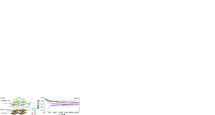
Here we present an x-ray absorption spectroscopy (XAS) study of the electric field doping of the well studied SrTiO3/NdBCO interface. The Cu edge (2 transition) XAS experiment was performed at the ID08 beam line of the European Synchrotron Radiation Facility. It was designed in order to allow simultaneous spectroscopic and transport characterization of the samples under the application of an electric field. Within the wide family of the HTS, NdBCO belongs to the “123” group, where, besides superconducting CuO2 planes, an important role is played by the CuO chains within the “charge reservoir” (CR). Transmission electron microscopy TEM has demonstrated that the first layer at the SrTiO3/NdBCO interface belongs to the CR, as sketched in Fig. 1a. This is particularly relevant since the effective electric field penetration calculated by a Thomas Fermi model or by any simple electrostatic estimates is of the order of 1 nm or less, i.e. less than one unit cell (u.c.). In previous studies the role of the atomic layers directly facing the interface was largely neglected. In this paper we will show, on the contrary, that they play a decisive role in the microscopic mechanism of the field effect doping of cuprates.

NdBCO (001) ultra-thin films have been epitaxially grown, by high oxygen pressure diode sputtering, on TiO2 terminated 10x10x 0.5 mm3 SrTiO3 (100) (STO) surface. The samples are pseudomorphic to the STO single crystals and have high structural perfection, and very smooth surfaces. The field effect structures have been completed by deposition on the thin film of the gold pads for transport measurements, and of the gate electrode ( mm2 area) on the back of the substrate, in a geometry suitable for the XAS experiment. The field has been applied through the SrTiO3 single crystal under ultra high vacuum conditions. The devices have been characterized in situ during the XAS experiment. A negative creates holes at the interface (accumulation mode) and a positive reduces the density of holes in the sample (depletion mode). The capacitance of this device is a function of the gate voltage, a well-known result for non-linear dielectrics materials like STO. At low gate voltage it is about 2.5 nF and it decreases to 0.4 nF at high voltages. The charge accumulated at the interface is consequently measured by an electrometer and is related to the capacitance and to the areal carrier density through the relation . With V, about holes/cm2 can be subtracted/added at the STO/NdBCO interface [see also EPAPS file].
We have studied NdBCO samples with a doping above and below the critical value separating the superconducting and insulating phases (Fig. 1b) SISAL . An example of the effect of the electric field is shown in Fig. 2. The resistivity of the 3 u.c. NdBCO sample at 10 K non-linearly decreases as function of , in agreement with the induction of carriers in the CuO2 planes. It is worth nothing that the field effect doping is insufficient to induce superconductivity. Similarly, we could not revert the 4 u.c. sample from superconducting to insulating by applying a positive gate voltage. These results are in contradiction with simple model expectations: assuming that only one unit cell is doped and that all the carriers are transferred to the CuO2 planes, about ppl=0.05 holes/CuO2 plane would be added or subtracted. In the 3 u.c. NdBCO the average hole population per CuO2 plane is 0.05(0), consequently the electric field should bring to zero the conduction carriers for V V and double them for V V. In such a scenario, an insulating to superconducting transition is expected, as shown in the inset of Fig. 2. Even assuming that all the unit cells are doped, a phase transition should occur anyhow in the samples studied, because the carrier density would change by 0.015 holes/CuO2, i.e., enough to induce a transition.
To unravel the underlying microscopic mechanism of the electric field effect, we have used the XAS technique that is sensitive to the orbital occupation and symmetry at the different copper sites of our samples. We collected the total electron yield signal that probes a depth of few nanometers, slightly larger than the NdBCO film thickness. By using the linear polarization of the x-rays, spectra corresponding to final states lying parallel or perpendicular to the CuO2 planes have been measured ( and spectra in Fig. 3) [see EPAPS file].
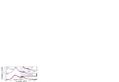
The Cu spectra, measured on the NdBCO films at 10 K, present the typical features of all cuprates, i.e., a main peak at 932.0 eV and a shoulder at 933.5 eV (Fig. 3) XAS1 . “123” cuprates contain two inequivalent copper sites, i.e., Cu(1) in the chains and Cu(2,3) in the CuO2 planes (see Fig. 1a). As shown in XAS2 and XASGHI , the main peak has a contribution from the doped Cu(1)3+in the chains that form a ligand state (3) with the neighboring oxygen ions, which increases if holes are injected in the chains along the axes. Another contribution comes from the undoped Cu(2,3)2+ in the CuO2 planes (state). The remaining doped Cu(2,3) sites, occupied by formally trivalent Cu(2,3)3+ ions, give rise to the satellite peak at 933.5 eV. In the spectra, this feature is due to the Zhang-Rice (ZR) singlet ZR , i.e., to the mobile carriers in the CuO2 planes. In the spectra the satellite is due to Cu(2,3)3+ sites hybridized with the apical O(4) oxygen, a signature of the charge transfer from the chains to the planes. As shown in Fig. 3 and in XASSAL , the satellite peaks decreases with the thickness of the NdBCO films, in agreement with the transport properties, with the reduction of the carrier density and of the charge transfer from the chains to the CuO2 plane.
The effects of the electric field on the spectra at 10 K are shown in Fig. 4 for the 3 u.c. sample, and similar result were found for the 2 u.c. and 4 u.c. films. Under negative (positive) gate voltages, the satellite at 933.5 eV, acquires (looses) spectral weight because the injected charges fill up (empty) the ZR band, i.e., additional carriers appear at the CuO2 planes. However, the largest effects are observed on the main peak, which shows a strong increase (decrease) in intensity and a gradual broadening (narrowing) on the high-energy side. As shown in Fig. 4b, where the spectrum at zero field is subtracted from the data, a peak at about 932.2 eV continuously grows with negative gate voltages. These results are explained by an enhancement of hole density along the chains by negative fields. The ratio of the holes induced in the chains (at the Cu(1) sites) and in the CuO2 planes (at the Cu(2,3) sites) as estimated from the integrated intensities around 932.2 eV and 933.5 eV in Fig. 4b, is . It does not depend on the gate voltage within the experimental error.
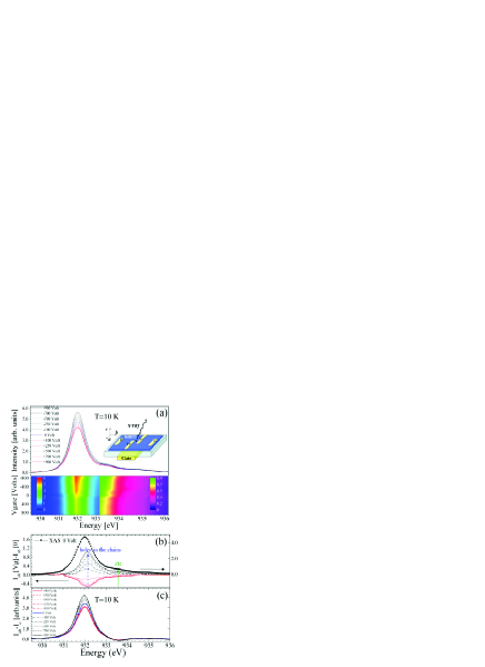
The electric field effect is similar in the plane and along the axis. However, interesting differences can be noted. In Fig. 4c we show the XAS () spectra as a function of the field: for negative (positive) gate voltages, the main peak at 932 eV acquires (looses) relative in-plane intensity, whereas the satellite anisotropy remains almost unaffected. This confirms that negative voltages lead to a strong enhancement of the hole population along the chains (parallel to the plane). On the contrary the filling of the ZR band is accompanied by an equal change of Cu(2,3)-O(4) ligand states. This is a further confirmation that the doping of the CuO2 planes is rather indirect, i.e., it occurs by a partial charge transfer from the heavily doped chains via the Cu(2,3)-O(4) bonding.
The XAS results are consistent with the transport data measured in situ and shown in Fig. 2. In particular we find a non-linear relationship between the change in the resistance and the weight of ZR states (proportional to the integrated intensity of the satellite peak) from Vgate=+1000 V to -500 V and a saturation (lower slope) at higher negative voltages. This resembles the non-linear relationship between the resistivity and induced carrier density shown in Fig. 2 and can be explained by taking into account the activated temperature dependence, with a slope depending on the carrier density, of the resistance in insulating cuprates.
The data are also consistent with previously published results. In “123” compounds shifts of up to 10 K where observed in samples not fully superconducting at 4.2 K FETAPLMAN ; FETPRLTRI . There the carrier doping at zero field was similar to ours (about 0.05 holes/CuO2 plane) and an increase of about 0.06 holes/CuO2 plane should have been expected at maximum field, corresponding to shift of greater than 30 K, instead of the 10 K observed. In Ref. FET3, similar differences between the measured shift in and the values expected from the injected carrier density are also reported NOTE2 .
In conclusion, our experimental results give the evidence that an external electric field injects holes mainly in the chains belonging to the charge reservoir, whereas only a fraction of them are transferred to the CuO2 planes by charge transfer from the charge reservoir to the CuO2 planes, which is the same mechanism governing the doping of the CuO2 planes by chemical substitution in the whole HTS family. This process is specific to the family of ”123” compounds, where the CR is composed by CuO chains. However it is likely that symilar scheme could operate in the case of other HTS, i.e. the electric field could modify the valence of the cations in the CR and by in this way could transfer holes to the CuO2 planes.
The similarity between electric field and chemical doping opens new perspectives for the investigation of the microscopic phase separation phenomena, proposed to be a key ingredient in the description of superconducting to insulator transitions of underdoped HTS SIECK . Indeed while the charge induced by field effect is homogeneously distributed within the gate area at the interface with the thin HTS film, the holes created by chemical doping are not, especially in the case of insulating or barely superconducting samples. The apparent similarities between field effect doping and chemical doping may thus suggest that collective electronic phase separation is necessary to accommodate doped holes in the parent undoped compounds. Further studies in this direction are required to confirm this hypothesis. Finally, our experiment clarifies that, to obtain a shift of of several degrees or a phase transition, a doping level substantially higher than usually achieved is necessary. On the other hand, by having identified the physical mechanisms leading to electric field doping of the CuO2 planes in the HTS, we have shown that an advanced interface engineering, i.e., the right choice of the atomic layers at the interface and their chemical and structural control, can eventually open the way to a more effective field-effect doping of high critical temperature superconductors.
Acknowledgements.
The Authors are grateful to Jean-Marc Triscone and to Antonio Barone for useful discussion about data interpretation. M. S., G. D. L. and R. V. acknowledge the support from the EU under the project Nanoxide, contract n. 033191.References
- (1) C. H. Ahn et al., Rev. Mod. Phys. 78, 1185 (2006)
- (2) A. Kevin Parendo, K. H. Sarwa, B. Tan, A. Bhattacharya, M. Eblen-Zayas , N. E. Staley, and A. M. Goldman, Phys. Rev. Lett. 94, 197004 (2005)
- (3) C. H. Ahn, J.-M. Triscone, and J. Mannhart, Nature 424, 1015 (2003)
- (4) C. H. Ahn, S. Gariglio, P. Paruch, T. Tybell, L. Antognazza, and J.-M. Triscone, Science 284, 1152 (1999)
- (5) D. Matthey, S. Gariglio, and J.-M. Triscone, Appl. Phys. Lett. 83, 3758 (2003)
- (6) J. Mannhart, D. G. Schlom, J. G.Bednorz, and K. A. Müller, Phys. Rev. Lett. 67, 2099 (1991); A. Walkenhorst, C. Doughty, , X. X. Xi, Qi Li , C. J. Lobb, S. N. Mao, and T. Venkatesan, Phys. Rev. Lett. 69, 2709 (1992)
- (7) A. Cassinese, G. M. De Luca, A. Prigiobbo, M. Salluzzo, and R. Vaglio, Appl. Phys. Lett. 84, 3933 (2004)
- (8) F. C. Zhang, and T. M. Rice, Phys. Rev. B 37, 3759 (1988)
- (9) J. B. Torrance, Y. Tokura, A. I. Nazzal, A. Bezinge, T. C. Huang, and S. S. P. Parkin, Phys. Rev. Lett. 61, 1127 (1988); Y. Ando, Y. Hanaki, S. Ono, T. Murayama, K. Segawa, N. Miyamoto, and S. Komiya, Phys. Rev. B 61, R14956 (2000)
- (10) G. Yu. Logvenova, C. W. Schneider, and J. Mannhart, Yu. S. Barash, Appl. Phys. Lett. 86, 202505 (2005)
- (11) D. Matthey, N. Reyren, and J.-M. Triscone, T. Schneider, Phys. Rev. Lett. 98, 057002 (2007)
- (12) Seongshik Oh, Maitri Warusawithana, and James N. Eckstein, Phys. Rev. B 70, 064509 (2004)
- (13) S. Bals, G. Van Tendeloo, M. Salluzzo, I. Maggio-Aprile, Appl. Phys. Lett. 79, 3660 (2001); S. Bals et al. Physica C 372-376, 711-714 (2002) and references therein.
- (14) M. Salluzzo, G. M. De Luca, D. Marré, M. Putti, M. Tropeano, U. Scotti di Uccio, and R. Vaglio, Phys. Rev. B 72, 134521 (2005)
- (15) H. Eskes, M. B. J. Meinders, and G. A. Sawatzky, Phys. Rev. Lett. 67, 1035 (1991); M. A. van Veenendaal, G. A. Sawatzky, Phys. Rev. B 49, 3473 (1994)
- (16) T. Mizokawa, T. Konishi, A. Fujimori, Z. Hiroi, M. Takano, and Y. Takeda, J. Electron Spectr. Rel. Phenomena 92, 97 (1998)
- (17) G. Ghiringhelli, N. B. Brookes, C. Dallera, A. Tagliaferri, and L. Braicovich, Phys. Rev. B 76, 085116 (2007)
- (18) M. Salluzzo, G. Ghiringhelli, , N. B. Brookes, G. M. De Luca, F. Fracassi and R. Vaglio, Phys. Rev. B 75, 054519 (2007)
- (19) In Ref. FET3, the Hall effect coefficient was used to extract the amount of carriers injected into the CuO2 planes. It is well known that in “123” compounds also the chains contribute to the transport, consequently the Hall coefficient depends also on the carrier present in the chains, and, in the case of a field effect experiment, on the carrier injected into the chains. Consequently, it is not surprising to find an agreement between the order of magnitude of the Hall effect coefficient and the estimated field effect injected carrier density.
- (20) Seongshik Oh, Trevis A. Crane, D. J. Van Harlingen, and J. N. Eckstein, Phys. Rev. Lett. 96, 107003 (2006)