Charge pumping in magnetic tunnel junctions: Scattering theory
Abstract
We study theoretically the charge transport pumped by magnetization dynamics through epitaxial FIF and FNIF magnetic tunnel junctions (F: Ferromagnet, I: Insulator, N: Normal metal). We predict a small but measurable DC pumping voltage under ferromagnetic resonance conditions for collinear magnetization configurations, which may change sign as function of barrier parameters. A much larger AC pumping voltage is expected when the magnetizations are at right angles. Quantum size effects are predicted for an FNIF structure as a function of the normal layer thickness.
A magnetic tunnel junction (MTJ) consists of a thin insulating tunnel barrier (I) that separates two ferromagnetic conducting layers (F) with variable magnetization direction.Zhang and Butler (2003) With a thin normal metal layer inserted next to the barrier, the MTJ is the only magnetoelectronic structure in which quantum size effects on electron transport have been detected experimentally.Yuasa et al. (2002) More importantly, MTJs based on transition metal alloys and epitaxial MgO barriers Yuasa et al. (2004); Parkin et al. (2004) are the core elements of the magnetic random-access memory (MRAM) devices Kawahara et al. (2007) that are operated by the current-induced spin-transfer torque. Slonczewski (1996); Berger (1996)
It is known that a moving magnetization of a ferromagnet pumps a spin current into an attached conductor.Tserkovnyak et al. (2002) Spin pumping can be observed indirectly as increased broadening of ferromagnetic resonance (FMR) spectra.Mizukami et al. (2002) The spin accumulation created by spin pumping can be converted into a voltage signal by an analyzing ferromagnetic contact.Berger (1999) This process can be divided into two steps: (1) the dynamical magnetization pumps out a spin current with zero net charge current, (2) the static magnetization (of the analyzing layer) filters the pumped spin current and gives a charge current. In the presence of spin-flip scattering, the spin-pumping magnet can generate a voltage even in an FN bilayer.Wang et al. (2006); Costache et al. (2006a) Spin-pumping by a time-dependent bulk magnetization texture such as a moving domain wall is also transformed into an electromotive force. Barnes and Maekawa (2007) Other experiments on spin-pumping induced voltages have also been reported. Azevedo et al. (2005); Saitoh et al. (2006)
Here we present a model study of spin-pumping induced voltages (charge pumping) in MTJs. Since the ferromagnets are separated by tunnel barrier, we cannot use the semiclassical approximations appropriate for metallic structures.Berger (1999); Brataas et al. (2000); Tserkovnyak et al. (2005); Wang et al. (2006) Instead, we present a full quantum mechanical treatment of the currents in the tunnel barrier by scattering theory. The high quality of MgO tunnel junctions and the prominence of quantum oscillations observed in FNIF structures (even for alumina barriers) provide the motivation to concentrate on ballistic structures in which the transverse Bloch vector is conserved during transport. For a typical MTJ under FMR with cone angle at frequency GHz, we find a DC pumping voltage of nV for collinear magnetization configurations or AC voltage with amplitude V for perpendicular configurations. The magnetization dynamics-induced voltages could give simple and direct access to transport parameters of high-quality MTJs, such as barrier height, magnetization anisotropies and damping parameters in a non-destructive way. The polarity of the pumping voltage can be changed by engineering the device parameters, etc. An oscillating signal as a function of the thickness of the N spacer leads to Fermi surface calipers that are in tunnel junctions not accessible via the exchange coupling.
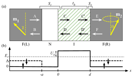
We consider a structure shown in Fig. 1(a), where two semi-infinite F leads (F(L) and F(R)) are connected by an insulating layer (I) of width and a non-magnetic metal layer (N) of width . The magnetization direction of F(L)/F(R), (), is treated as fixed/free. We disregard any spin accumulation in F, thus treat them as ideal reservoirs in thermal equilibrium. This is allowed when the spin pumping current is much smaller than the spin-flip rate in the ferromagnet, which is usually a good approximations. The structure reduces to an FIF MTJ when . Let be the spin-dependent amplitudes () at specific points (see Fig. 1) of flux-normalized spinor wave-functions. The scattering states can be expressed in terms of the incoming waves and , such as:
| (1) |
where and are matrices in spin space and can be calculated by concatenating the scattering matrices of region and of the bulk layer I. To first order of the transmission () through the bulk I,
| (2) |
where / are the transmission/reflection matrices for (see Fig. 1), the hatless are the spin-independent transmission/reflection coefficient for the insulating bulk I. The primed and unprimed version specify the scattering of electrons emitted coming from the left and right, respectively. The reflection coefficient is due to the impurity scattering inside the bulk I, and its magnitude mainly depends on the impurity density in I, especially near the interfaces. All scattering coefficients are matrices in the space of transport channels at the Fermi energy that are labeled by the transverse wave vectors in the leads: (the band index is suppressed).
The response to a small applied bias voltage can be written as with conductance :
| (3) |
where denotes the spin trace and the summation is over all transverse modes in the leads at the Fermi level.
When the structure is unbiased but the magnetic configuration is time-dependent, a spin current is pumped through the structure. Tserkovnyak et al. (2002) When the dynamics is slow, , it can be treated by the theory of adiabatic quantum pumping. Büttiker et al. (1994) We consider a situation in which the magnetization () of one layer precesses with velocity around the -axis with constant cone angle , whereas the other magnetization () is constant (see Fig. 1). We focus on the charge current that accompanies the spin pumping:
| (4) | ||||
When a DC current is blocked (open circuit), a voltage bias builds up
| (5) |
The discussion above is valid for general scattering matrices that e. g. include bulk and interface disorders. In order to derive analytical results, we shall make some approximations. First of all, we assume that spin is conserved during the scattering, for (, similar for ) is collinear with : Tserkovnyak et al. (2002) Expanded in Pauli matrices , , with . () is the transmission amplitude for spin-up/down electrons with spin quantization axes in the scattering region . In the absence of impurities (), Eq. (2) becomes
| (6) | ||||
Since all hatless quantities in this equation are still matrices in -space, such as , the order of as in Eq. (2) should be maintained. The term in Eq. (4) may be disregarded, because only the part of that depends on both and contributes to , and that part is in higher order of .
Another approximation is the free electron approximation tailored for transition metal based ferromagnets.Slonczewski (1989) We assume spherical Fermi surfaces for spin-up and spin-down electrons (in both F(L) and F(R)) with Fermi wave-vectors and , with an effective electron mass in F. Electrons in N are assumed to be ideally matched with the majority electrons in F (). Let and be the barrier height of and effective mass in the tunnel barrier. The adopted potential profile is shown in Fig. 1(b). We assume the transverse wave-vector to be conserved () by disregarding any impurity or interface roughness scattering, which means the scattering matrices () are diagonal in -space. With these approximations, the double summation in Eqs. (3, 4) is replaced by a single integration over transverse wave-vectors. The scattering amplitudes and can be calculated by matching the flux-normalized wave-functions at the interfaces. The transmission coefficient in the barrier bulk is the exponential decay: with . Then we obtain our main result from Eq. (6):
| (7a) | ||||
| (7b) | ||||
where is the total transmission probability for scattering region , and with polarization . In Eq. (7b), The term in the square brakets is the transmitted spin pumping current, and represents the filtering by the static layer that converts the spin into a charge current.
For an Fe/MgO/Fe MTJ: Å-1 and Å-1 for Fe,Slonczewski (1989) and eV and for MgO. Yuasa et al. (2004); Moodera and Kinder (1996) This implies eV, eV , and ( when and nm). For an FIF structure (), both and contain only a single F(L)/I (for ) or I/F(R) (for ) interface. From the potential profile in Fig. 1(b),
| (8) |
for and zero otherwise.
If precesses about an axis that is parallel to ( or , see Fig. 1) and the second term in Eq. (7b) vanishes. The dot product is time-independent, thus generates a DC signal. Let us consider an FIF MTJ with barrier width nm, with precessing around the -axis at frequency GHz with cone angle . We find a DC charge pumping voltage over the F leads nV when is parallel to the precession axis () and nV when anti-parallel (). FNF is higher for the anti-parallel configuration simply because its resistance is higher. When the precession cone angle , Costache et al. (2006b) the DC voltage nV, similar to a previously measured pumping voltage in a metallic junction. Costache et al. (2006a)
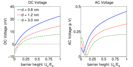
Fig. 2(a) shows the DC as a function of the barrier height for an FIF structure at and GHz. increases as a function of barrier height mainly because increases as a function of : From Eq. (7), we have (assume ). The first ratio , increases as a function of through , whereas second ratio is independent of . The pumping voltage therefore increases with (and ). We also see that decreases when increases, which can be understood by the following: The effect of the tunnel barrier is to focus the transmission electrons on small ’s due to the exponential decay factor . Smaller implies larger kinetic energy normal to the barrier and therefore reduced sensitivity to the spin-dependent potentials. Hence, decreases with barrier width. The lowest curve in Fig. 2(a) is approximately , because for large the electrons near completely dominate the transmission. The negative value of in Fig. 2(a) is caused by the negative polarization () at low barrier height for electrons with small . remains finite for infinitely high or wide barrier, however, the time to build up this voltage, the RC time (), goes to infinity due to the exponential growth of the resistance.
When is perpendicular to the precession axis of , i.e. , the charge pumping voltage oscillates around zero because both dot products in Eq. (7b), and , give rise to an AC signal. With , where the two components are out of phase by , the amplitude is given by . An FMR with and GHz then gives an AC pumping voltage with amplitude as large as V. Fig. 2(b) shows the barrier height dependence of amplitude quite similar to the DC case in Fig. 2(a) and for similar reasons. For a half metallic junction, the magnitude of the DC pumping voltage can be shown to be bounded by and AC pumping voltage amplitude must be smaller than , where .
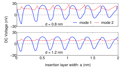
When an N layer of thickness is inserted, it is interesting to inspect the two different modes, mode 1: FNI and mode 2: NIF, where indicates the F layer under FMR. Eq. (7b) applies to mode 1, and applies to mode 2 with subscript 1 and 2 swapped. The N layer forms a quantum well for spin-down electrons that causes the oscillation in the charge pumping voltage as a function of as shown in Fig. 3. The period of the quantum oscillation due to the N insertion layer is about Å. However, due to the aliasing effect caused by the discrete thickness of the N layer, Chappert and Renard (1991) the observed period should be , where is the thickness of a monolayer. In mode 1, the quantum well formed by the N layer can modulate such that the electrons contributing to the transmission the most have () or (), and thus change the sign of the pumping voltage . On the other hand, there is no sign change in mode 2 because is independent of . Similar oscillations could also be found for the amplitude of the AC pumping voltage.
Because the AC voltage is proportional to and DC voltage is proportional to , the AC pumping voltage is much larger than the DC counterpart at small . However, in order to observe an AC pumping voltage, the time to build up the voltage, the RC time , has to be shorter than the pumping period, i.e. . Approximately , where and are the dielectric constant and electric constant, respectively. A more accurate estimation of the RC time for a typical structure is as follows: the resistance-area () value of the MTJ in our calculation is m2 for nm (m2 for nm, which is consistent with experimental values. Yuasa et al. (2004)) The capacitance of an MgO tunnel barrier with nm is calculated by F/m2 ( for MgO). Therefore ps ps. The electromagnetic response is therefore sufficiently fast to follow the AC pumping signal.
We ignored interface roughness and barrier disorder in the calculation of the pumping voltage. This may be justified by the high quality of epitaxial MgO tunnel barrier. Yuasa et al. (2004); Parkin et al. (2004) Furthermore, the geometric interface roughness mainly reduces the nominal thickness of the barrier Zhang and Levy (1999) which can be taken care of by an effective thickness parameter. Impurity states in the barrier open additional tunneling channels with , which generally increases tunneling but also reduces the spin-dependent effects when spin-flip is involved. In general, interface roughness and disorder can be important quantitatively, but have been shown not to qualitatively affect the features predicted by a ballistic model. Itoh et al. (1999) In order to be quantitatively reliable, the real electronic structure has to be taken into account as well. Both band structure and disorder effects can be taken into account by first-principles electronic structure calculation as demonstrated in for metallic structures. Zwierzycki et al. (2005)
Recently, a magnetization-induced electrical voltage of the order of V was measured for an FIN structure by Moriyama et al. Moriyama et al. (2008) The authors explain their findings by spin pumping, but note that the signal is larger than expected. An FMR generated electric voltage generation up to V was theoretically predicted for such FIN structures. Chui and Lin (2007) Surprisingly, this voltage is much larger than V, the maximum “intrinsic ”energy scale in spin-pumping theory.
To summarize, a scattering matrix theory is used to calculate the charge pumping voltage for a magnetic multilayer structure. An experimentally accessible charge pumping voltage is found for an FIF MTJ, the pumping voltage can be either DC or AC depending on the magnetization configurations. In FNIF structure we find on top of the previously reported oscillating TMR Yuasa et al. (2002) a charge pumping voltage that oscillates and may change sign with the N layer thickness.
This work has been supported by EC Contract IST-033749 “DynaMax”.
References
- Zhang and Butler (2003) X. G. Zhang and W. H. Butler, J. of Phys.: Cond. Matt. 15, 1603 (2003). E. Y. Tsymbal, O. N. Mryasov, and P. R. LeClair, J. of Phys.: Cond. Matt. 15, 109 (2003).
- Yuasa et al. (2002) S. Yuasa, T. Nagahama, and Y. Suzuki, Science 297, 234 (2002).
- Yuasa et al. (2004) S. Yuasa, T. Nagahama, A. Fukushima, Y. Suzuki, and K. Ando, Nature Materials 3, 868 (2004).
- Parkin et al. (2004) S. S. P. Parkin, C. Kaiser, A. Panchula, P. M. Rice, B. Hughes, M. Samant, and S.-H. Yang, Nature Materials 3, 862 (2004).
- Kawahara et al. (2007) T. Kawahara, R. Takemura, K. Miura, et al., Solid-State Circuits Conference, 2007. ISSCC 2007. Digest of Technical Papers. IEEE Inter. 480, (2007). M. Hosomi, H. Yamagishi, T. Yamamoto, et al., Electron Devices Meeting, 2005. IEDM Technical Digest. IEEE Inter. 459, (2005).
- Slonczewski (1996) J. C. Slonczewski, J. Magn. Magn. Mater. 159, L1 (1996).
- Berger (1996) L. Berger, Phys. Rev. B 54, 9353 (1996).
- Tserkovnyak et al. (2002) Y. Tserkovnyak, A. Brataas, and G. E. W. Bauer, Phys. Rev. Lett. 88, 117601 (2002).
- Mizukami et al. (2002) S. Mizukami, Y. Ando, and T. Miyazaki, Phys. Rev. B 66, 104413 (2002).
- Berger (1999) L. Berger, Phys. Rev. B 59, 11465 (1999).
- Wang et al. (2006) X. H. Wang, G. E. W. Bauer, B. J. van Wees, A. Brataas, and Y. Tserkovnyak, Phys. Rev. Lett. 97, 216602 (2006).
- Costache et al. (2006a) M. V. Costache, M. Sladkov, S. M. Watts, C. H. van der Wal, and B. J. van Wees, Phys. Rev. Lett. 97, 216603 (2006a).
- Barnes and Maekawa (2007) S. E. Barnes and S. Maekawa, Phys. Rev. Lett. 98, 246601 (2007). R. A. Duine, Phys. Rev. B 77, 014409 (2008). W. M. Saslow, Phys. Rev. B 76, 184434 (2007). M. Stamenova, T. N. Todorov, and S. Sanvito, Phys. Rev. B 77, 054439 (2008). S. A. Yang, D. Xiao, and Q. Niu, arXiv:0709.1117v2 (2007). Y. Tserkovnyak and M. Mecklenburg, arXiv:0710.5193 (2007).
- Azevedo et al. (2005) A. Azevedo, L. H. V. Leao, R. L. Rodriguez-Suarez, A. B. Oliveira, and S. M. Rezende, J. Appl. Phys. 97, 10 (2005).
- Saitoh et al. (2006) E. Saitoh, M. Ueda, H. Miyajima, and G. Tatara, Appl. Phys. Lett. 88, 182509 (2006).
- Brataas et al. (2000) A. Brataas, Y. V. Nazarov, and G. E. W. Bauer, Phys. Rev. Lett. 84, 2481 (2000).
- Tserkovnyak et al. (2005) Y. Tserkovnyak, A. Brataas, G. E. W. Bauer, and B. I. Halperin, Rev. of Mod. Phys. 77, 1375 (2005).
- Büttiker et al. (1994) M. Büttiker, H. Thomas, and A. Pretre, Zeit. Phys. B 94, 133 (1994). P. W. Brouwer, Phys. Rev. B 58, R10135 (1998).
- Slonczewski (1989) J. C. Slonczewski, Phys. Rev. B 39, 6995 (1989).
- Moodera and Kinder (1996) J. S. Moodera and L. R. Kinder, J. Appl. Phys. 79, 4724 (1996). M. Bowen, V. Cros, F. Petroff, A. Fert, C. M. Boubeta, J. L. Costa-Krämer, J. V. Anguita, A. Cebollada, F. Briones, J. M. d. Teresa, et al., Appl. Phys. Lett. 79, 1655 (2001). J. Faure-Vincent, C. Tiusan, C. Bellouard, E. Popova, M. Hehn, F. Montaigne, and A. Schuhl, Phys. Rev. Lett. 89, 107206 (2002).
- (21) For comparison, the DC voltage for a metallic FNF spin valve under same FMR is V in our calculation.
- Costache et al. (2006b) M. V. Costache, S. M. Watts, M. Sladkov, C. H. van. der. Wal, and B. J. van. Wees, Appl. Phys. Lett. 89, 232115 (2006b).
- Chappert and Renard (1991) C. Chappert and J. P. Renard, Europhys. Lett. 15, 553 (1991).
- Zhang and Levy (1999) S. Zhang and P. M. Levy, Euro. Phys. J. B 10, 599 (1999).
- Itoh et al. (1999) H. Itoh, A. Shibata, T. Kumazaki, J. Inoue, and S. Maekawa, J. Phys. Soc. Jpn. 68, 1632 (1999). J. Mathon and A. Umerski, Phys. Rev. B 60, 1117 (1999). H. Itoh, J. Inoue, A. Umerski, and J. Mathon, Phys. Rev. B 68, 174421 (2003). P. X. Xu, V. M. Karpan, K. Xia, M. Zwierzycki, I. Marushchenko, and P. J. Kelly, Phys. Rev. B 73, 180402(R) (2006).
- Zwierzycki et al. (2005) M. Zwierzycki, Y. Tserkovnyak, P. J. Kelly, A. Brataas, and G. E. W. Bauer, Phys. Rev. B 71, 064420 (2005).
- Moriyama et al. (2008) T. Moriyama, R. Cao, X. Fan, G. Xuan, B. K. Nikolić, Y. Tserkovnyak, J. Kolodzey, and J. Q. Xiao, Phys. Rev. Lett. 100, 067602 (2008).
- Chui and Lin (2007) S. T. Chui and Z. F. Lin, arXiv:0711.4939v1 (2007).