Sculptured–thin–film Plasmonic–Polaritonics
Abstract
The solution of a boundary–value problem formulated for the Kretschmann configuration shows that the phase speed of a surface–plasmon–polariton (SPP) wave guided by the planar interface of a sufficiently thin metal film and a sculptured thin film (STF) depends on the vapor incidence angle used while fabricating the STF by physical vapor deposition. Furthermore, it may be possible to engineer the phase speed by periodically varying the vapor incidence angle. The phase speed of the SPP wave can be set by selecting higher mean value and/or the modulation amplitude of the vapor incidence angle.
1 Introduction
A resonance phenomenon arises from the interaction of light with free electrons at a planar metal–dielectric interface [1, 2]. Under certain conditions, the energy carried by photons in the dielectric medium is transferred to collective excitations of free electrons in the metal. Because the free electrons in the metal are coupled to the photons in the dielectric medium, the quantum is called a surface plasmon polariton, often shortened to surface plasmon. A classical understanding of the surface plasmon polariton (SPP) is in terms of a electromagnetic surface wave that propagates along the interface and decays exponentially with distance normal to the interface.
Research on electromagnetic surface waves has a long history, dating back about a hundred years. Zenneck [3] proposed in 1907 a mode of electromagnetic wave propagation localized at the Earth–atmosphere interface. The wave, since named the Zenneck wave, propagates parallel to the interface with an amplitude which decays exponentially with distance from the interface. Credit is also given to Sommerfeld for a clean analysis of the phenomenon published in 1909 [4]. Basically the same kind of wave at optical frequencies, the SPP wave became the subject of intense investigation[5, 6, 7] from the middle part of the 20th century. It was soon realized that, because SPP waves are highly sensitive to conditions at the interface, they might be employed to detect various chemical species. SPP–wave–detection techniques are currently used for a wide range of sensing applications especially in the detection of biomolecules [8, 9, 10, 11].
Much of the SPP literature is restricted to the planar interface of a good conductor and an isotropic dielectric medium, though there are noticeable exceptions wherein the dielectric medium could be anisotropic [12, 13] and be additionally endowed with magnetic properties [14, 15, 16]. The SPP wave is excited through one of several different types of couplers [17].

In the Kretschmann [18] configuration, the bulk metal is in the form of a sufficiently thin film of uniform thickness, bounded by dielectric mediums on both sides, one medium being optically denser than the other. A plane wave is launched in the optically denser dielectric medium towards the metal film, in order to excite a surface–plasmon wave at the interface of the metal with the optically rarer dielectric medium. The plane wave must be –polarized. The telltale sign is a sharp peak in absorbance (i.e., a sharp trough in reflectance without a compensatory peak in transmittance) as the angle of incidence (with respect to the thickness direction) of the launched plane wave is changed. The absorbance peak occurs in the vicinity of the critical angle (of incidence) that would exist if the metal film were absent.
Generally, the optically rarer medium is homogeneous normal to its planar interface with the metal film, at least within the range of the SPP field. In this paper, however, we take the optically rarer medium to be continuously nonhomogeneous in the thickness direction. Specifically, this medium is a sculptured thin film (STF).
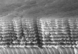
STFs are nanostructured materials with unidirectionally varying continuum properties that can be designed and realized in a controllable manner using physical vapor deposition [19]. The ability to virtually instantaneously change the growth direction of their columnar morphology, through simple variations in the direction of the incident vapor flux, leads to a wide variety of –nm–diameter columns of two– or three–dimensional shapes, as illustrated by the scanning electron micrographs in Figs. 1 and 2. At visible and infrared wavelengths, a STF is a unidirectionally nonhomogeneous continuum with direction–dependent properties.
This paper is organized as follows. Section 2 begins with a description of the Kretschmann configuration to launch a SPP wave at the planar interface of a metal and a STF. The relative permittivity dyadic of the STF is described in that section, along with the boundary–value problem to determine planewave absorbance. Section 3 contains numerical results to elucidate the effects of the nonhomogeneity of the STF on the SPP wave. An time–dependence is implicit, with denoting the angular frequency. The free–space wavenumber, the free–space wavelength, and the intrinsic impedance of free space are denoted by , , and , respectively, with and being the permeability and permittivity of free space. Vectors are in boldface, dyadics underlined twice; column vectors are in boldface and enclosed within square brackets, while matrixes are underlined twice and similarly bracketed. Cartesian unit vectors are identified as , and .
2 Theory
In conformance with the Kretschmann configuration [18, 20] for launching SPP waves, the half–space is occupied by a homogeneous, isotropic, dielectric material with the relative permittivity scalar . Dissipation in this material is considered to be negligible and its refractive index is real–valued and positive. The laminar region is occupied by a bulk metal with relative permittivity scalar . The region is occupied by a STF. Without significant loss of generality in the present context, the half–space is taken to be occupied by the same material as fills the half–space .
2.1 Sculptured Thin Film
The relative permittivity dyadic of the STF is factorable as
| (1) |
wherein the reference relative permittivity dyadic
| (2) |
captures the locally orthorhombic character of STFs, the dyadic function
| (3) |
denotes rotation about the axis, the dyadic function
| (4) |
involves the angle , and the superscript T denotes the transpose. The quantities , , , , and can all be functions of .
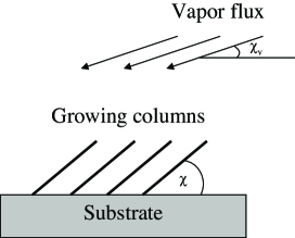
Although STFs have been made by evaporating a wide variety of materials [19, 21], the constitutive parameters of STFs have not been extensively measured. However, the constitutive parameters of certain columnar thin films (CTFs) are known. Both CTFs and STFs are fabricated by physical vapor deposition. The basic procedure to deposit CTFs has been known for more than a century. At low enough temperature and pressure, a solid material confined in a boat evaporates towards a stationary substrate. The vapor flux is collimated into a well–defined beam, and its average direction is quantified by the angle with respect to the substrate plane, as illustrated in Fig. 3. Provided the adatom mobility is low, the resulting film turns out to be an assembly of parallel and nominally identical columns. The columns have elliptical cross–sections and are tilted at an angle with respect to the substrate plane. The parameters , , , and have to be functions of , at the very least because the nanoscale porosity of a CTF depends on the direction of the vapor flux.
A series of optical characterization experiments on certain CTFs were carried out some years ago [22, 23]. After ignoring the effects of dispersion and dissipation, at least in some narrow range of frequencies, the results can be put in the following form for our present purposes:
| (5) |
Here, is the vapor incidence angle expressed as a fraction of a right angle. The quantities and , etc., in Eq. 5 depend on the evaporant material as well as the deposition conditions.
When the substrate is rotated about either the or the axes, parallel columns of specific shape grow instead of straight columns, and a STF is deposited instead of a CTF. Although the substrate is nonstationary, the functional relationships connecting , , , and to for CTFs would substantially apply for STFs, provided the substrate rotation is sufficiently slow. Thus, we need only to specify the –dependences of and .
For our present purposes, we chose
| (6) |
Here, is a characteristic length along the axis, whereas the angles and . The structural–handedness parameter for right–handedness, for left–handedness, and for no handedness. For theoretical investigations, we decided to focus on the following three types of STFs:
-
(i)
columnar thin films (, );
-
(ii)
sculptured nematic thin films with periodically varying tilt angle (, ); and
-
(iii)
chiral sculptured thin films (, ).
2.2 Boundary–Value Problem
Suppose that a –polarized plane wave, propagating in the half–space at an angle to the axis in the plane, is incident on the metal–coated STF in the Kretschmann configuration. The electric field phasor associated with the incident plane wave is
| (7) |
The reflected electric field phasor is expressed as
| (8) |
and the transmitted electric field phasor as
| (9) |
Here,
| (10) |
where is the phase speed parallel to the interfacial plane of interest, and the unit vectors and denote the – and the –polarization states of the electric field phasors.
The reflection amplitudes and , as well as the transmission amplitudes and , have to be determined by the solution of a boundary–value problem. The required procedure is standard [19]. It suffices to state here that the following set of four algebraic equations emerges (in matrix notation):
| (15) | |||
| (20) |
The procedure to obtain the 44 matrix can be gleaned from two predecessor papers [24, 25]. The remaining two 44 matrixes in Eq. 20 are as follows:
| (21) |
| (31) | |||||
Equation 20 can be solved for , , , and using standard algebraic techniques. The quantity of interest for establishing the existence of the SPP wave is the absorbance
| (32) |
as a function of .
3 Numerical Results and Discussion
Calculations of against are reported in this paper for the following parameters of the STF: nm, , and . Calculations have shown that the selection of higher values of does not impact the SPP wave significantly, whereas the effect of the nanostructured periodicity of SNTFs and chiral STFs is not appreciable for lower values of . The free–space wavelength nm is the same at which the parameters in Eqs. 5 were measured. The STF was taken to be made of titanium oxide: , , , , , , , , , and [22]. The metal was chosen to be aluminum: [26] and nm. The metal film is thus thin enough that it allows sufficient penetration of the evanescent wave to excite the SPP at the metal–STF interface; at the same time, the metal film is thus thick enough to prevent tunneling of photons across it from the medium of incidence and reflection to the STF. The two half–spaces were taken to be filled with zinc selenide (), which is optically denser than all three types of STFs considered here.
Let us begin with the case of the metal–backed CTF: and . Figure 4 shows as a function of . The SPP wave is excited at , with the absorbance in excess of denoting a very efficient conversion of the energy of the incident plane wave into the SPP wave.
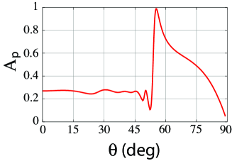
Let denote the value of at which the SPP wave is excited. A study of versus reveals that for a CTF fabricated with a specific evaporant material increases as increases [27]. Therefore, the wavenumber of the SPP wave, given by
| (33) |
is a monotonically increasing function of , which means that the phase speed
| (34) |
of the SPP wave is a monotonically decreasing function of .
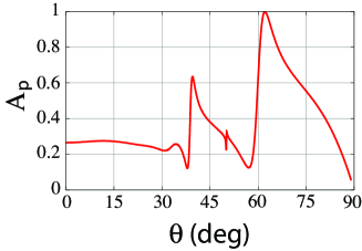
The effect of nonhomogeneity in the dielectric medium on the SPP wave becomes evident when we consider the metal–backed sculptured nematic thin film: and . Figure 5 shows as a function of when . The SPP wave is excited at , with the absorbance in excess of . A comparison of Figs. 4 and 5 suggests that the phase speed of the SPP wave decreases when the vapor incidence angle is periodically modulated with a significant amplitude, but the high efficiency of conversion of the energy of the incident plane wave into the SPP wave is not affected thereby.

Nonhomogeneity is also introduced in the dielectric medium when the vapor deposition angle is held fixed during fabrication but the substrate is rotated about the axis. Figure 6 shows as a function of when and ; i.e., it is drawn for a metal–backed chiral STF. Now, , which is only marginally higher than in Fig. 4.
4 Concluding Remarks
We conclude that the solution of a boundary–value problem formulated for the Kretschmann configuration shows that the phase speed of a SPP wave guided by the planar interface of a sufficiently thin metal film and a sculptured thin film depends on the vapor incidence angle used while fabricating the STF by physical vapor deposition. Therefore, it may be possible to engineer the phase speed quite simply by selecting an appropriate value of the vapor incidence angle (in addition to the metal and the evaporant species). Furthermore, by periodically varying the vapor incidence angle, the phase speed of the SPP wave can be reduced. Adequate selection of the phase speed should be important for controlled data flow in plasmonic circuits.
The high degree of porosity [19] of STFs may provide certain advantages in the application of SPP waves in detectors. A properly chosen STF could prevent particulates from reaching its interface with the metal film while allowing molecular species through for detection. The detection of biomolecules typically relies on recognition molecules, which are bound to the interface, binding with the analyte molecules. The porosity and surface roughness of the STF may offer some advantage for adherence of the recognition molecule. STFs can now be patterned using standard photolithographic techniques [28]. Partitioning of the STF into many sectors could permit the use of multiple species of recognition molecules on a single chip for the detection of many different types of analyte molecules. Recently, the activity of living cells has been monitored using SPP detection techniques [29]. Cells have been shown to grow well on the rough STF surface [21, 30], which thus may offer an advantage. Finally, titanium oxide is a very well–known photocatalyst. Although the photocatalytic properties of titanium oxide STFs [31, 32] have been investigated, the combination of SPP detection and this catalyst may allow for other useful applications to emerge.
References
- [1] A. V. Zayats, I. I. Smolyaninov, and A. A. Maradudin, “Nano–optics of surface plasmon polaritons,” Phys. Rep., vol. 408, pp. 131–314, 2005.
- [2] J. M. Pitarke, V. M. Silkin, E. V. Chulkov, and P. M. Echenique, “Theory of surface plasmons and surface–plasmon polaritons,” Rep. Prog. Phys., vol. 70, pp. 1–87, 2007.
- [3] J. Zenneck, “Über die Fortpflanzung ebener elektromagnetischer Wellen längs einer ebenen Lieterfläche und ihre Beziehung zur drahtlosen Telegraphie,” Ann. Phys. Lpz., vol. 23. pp. 846–866, 1907.
- [4] A. Sommerfeld, “Über die Ausbreitlung der Wellen in der drahtlosen Telegraphie,” Ann. Phys. Lpz., vol. 28, pp. 665–736, 1909.
- [5] H. Raether, Surface Plasmons on Smooth and Rough Surfaces and on Gratings. New York, NY, USA: Springer, 1983.
- [6] V. M. Agranovich and D. L. Mills (eds.), Surface Polaritons: Electromagnetic Waves at Surfaces and Interfaces. Amsterdam, The Netherlands: North–Holland, 1982.
- [7] A. D. Boardman (ed.), Electromagnetic Surface Modes. Chichester, United Kingdom: Wiley, 1982.
- [8] B. Liedberg, I. Lundstörm, and E. Stenberg, “Principles of biosensing with an extended coupling matrix and surface plasmon resonance,” Sens. Actuat. B: Chem., vol. 11, pp. 63–72, 1993.
- [9] J. Homola, S. S. Yee, and G. Gauglitz, “Surface plasmon resonance sensors: review,” Sens. Actuat. B: Chem., vol. 54, pp. 3–15, 1999.
- [10] S. A. Kalele, N. R. Tiwari, S. W. Gosavi, and S. K. Kulkarni, “Plasmon–assisted photonics at the nanoscale,” J. Nanophoton., vol. 1, art no. 012501, 2007.
- [11] I. Abdulhalim, M. Zourob, and A. Lakhtakia, “Surface plasmon resonance for biosensing: A mini–review,” Electromagnetics, vol. 28, 2008 (at press).
- [12] R. F. Wallis, J. J. Brion, E. Burstein, and A. Hartstein, “Theory of surface polaritons in anisotropic dielectric media with application to magnetoplasmons in semiconductors,” Phys. Rev. B, vol. 9, pp. 3424–3437, 1974.
- [13] D. Mihalache, D.–M. Baboiu, M. Ciumac, L. Torner, and J. P. Torres, “Hybrid surface plasmon polaritons guided by ultrathin metal films,” Opt. Quantum Electron., vol. 26, pp. 857–863, 1994.
- [14] A. Hartstein, E. Burstein, A. A. Maradudin, R. Brewer, and R. F. Wallis, “Surface polaritons on semi–infinite gyromagnetic media,” J. Phys. C: Solid State Phys., vol. 6, pp. 1266–1276, 1973.
- [15] A. N. Furs and L. M. Barkovsky, “A new type of surface polaritons at the interface of the magnetic gyrotropic media,” J. Phys. A: Math. Theor., vol. 40, pp. 309–328, 2007.
- [16] W. Yan, L. Shen, L. Ren, and J. A. Kong, “Surface modes at the interfaces between isotropic media and indefinite media,” J. Opt. Soc. Am. A, vol. 24, pp. 530–535, 2007.
- [17] W. Knoll, “Interfaces and thin films as seen by bound electromagnetic waves,” Annu. Rev. Phys. Chem., vol. 49, pp. 569–638, 1998.
- [18] E. Kretschmann and H. Raether, “Radiative decay of nonradiative surface plasmons excited by light,” Zeit. Naturforsch. A, vol. 23, pp. 2135–2136, 1968.
- [19] A. Lakhtakia and R. Messier, Sculptured Thin Films: Nanoengineered Morphology and Optics. Bellingham, WA, USA: SPIE Press, 2005.
- [20] H. J. Simon, D. E. Mitchell, and J. G. Watson, “Surface plasmons in silver films—a novel undergraduate experiment,” Am. J. Phys., vol. 43, pp. 630–636, 1975..
- [21] A. Lakhtakia, M. C. Demirel, M. W. Horn, and J. Xu, “Six emerging directions in sculptured–thin–film research,” Adv. Solid State Phys., vol. 46, pp. 295–307, 2008.
- [22] I. J. Hodgkinson, Q. h. Wu, and J. Hazel, “Empirical equations for the principal refractive indices and column angle of obliquely deposited films of tantalum oxide, titanium oxide, and zirconium oxide,” Appl. Opt., vol. 37, pp. 2653–2659, 1998.
- [23] I. J. Hodgkinson, Q. h. Wu, and S. Collett, “Dipsersion equations for vacuum–deposited tilted columnar biaxial media,” Appl. Opt., vol. 40, pp. 452–457, 2001.
- [24] J. A. Polo Jr. and A. Lakhtakia, “Sculptured nematic thin films with periodically modulated tilt angle as rugate filters,” Opt. Commun., vol. 251, pp. 10–22, 2005.
- [25] A. Lakhtakia, “Surface–plasmon wave at the planar interface of a metal film and a structurally chiral medium,” Opt. Commun., vol. 279, pp. 291–297, 2007.
- [26] M. Mansuripur and L. Li, “What in the world are surface plasmons?,” OSA Opt. Photon. News, vol. 8, no. 5, pp. 50–55 (1997).
- [27] A. Lakhtakia and J. A. Polo, Jr., “Morphological influence on surface–wave propagation at the planar interface of a metal film and a columnar thin film,” Asian J. Phys., vol. 17, 2008 (at press); also: arXiv:0706.4306.
- [28] M. W. Horn, M. D. Pickett, R. Messier, and A. Lakhtakia, “Selective growth of sculptured nanowires on microlithographic substrates,” J. Vacuum Sci. Technol. B, vol. 22, pp. 3426–3430, 2004.
- [29] R. Ziblat, V. Lirtsman, D. Davidov, and B. Aroeti, “Infrared surface plasmon resonance: A novel tool for real time sensing of variations in living cells,” Biophys. J., vol. 90, pp. 2592–2599, 2006.
- [30] M. C. Demirel, E. So, T. Ritty, S. H. Naidu, and A. Lakhtakia, “Nanoengineered sculptured thin films for fibroblast cell attachment and growth,” J. Biomed. Mater. Res. B, vol. 81, pp. 219–223, 2007.
- [31] M. Suzuki, T. Ito, and Y. Taga, “Photocatalysis of sculptured thin films of TiO2,” Appl. Phys. Lett., vol. 78, pp. 3968–8970, 2001.
- [32] B. R. Weinberger and R. B. Garber, “Titanium dioxide photocatalysts produced by reactive magnetron sputtering,” Appl. Phys. Lett., vol. 66, pp. 2409–2411, 1995.