Valley interference effects on a donor electron close to a Si/SiO2 interface.
Abstract
We analyze the effects of valley interference on the quantum control and manipulation of an electron bound to a donor close to a Si/SiO2 interface as a function of the valley-orbit coupling at the interface. We find that, for finite valley-orbit coupling, the tunneling times involved in shuttling the electron between the donor and the interface oscillate with the interface/donor distance in much the same way as the exchange coupling oscillates with the interdonor distance. These oscillations disappear when the ground state at the interface is degenerate (corresponding to zero valley-orbit coupling).
pacs:
03.67.Lx, 85.30.-z, 73.20.Hb, 85.35.Gv, 71.55.CnI Introduction
Miniaturization of the traditional Si transistors is, after decades, still following the time-defying Moore’s law, with a reduction in size every two years. Soon the effects of dopants disorder in the transistors threshold voltage will be important Shinada et al. (2005) and, in a few years, their behavior will be dominated by quantum effects. These technical improvements can be used in the advancement of one of the promising candidates for the physical implementation of a quantum computer: doped Si. Kane (1998); Vrijen et al. (2000); Skinner et al. (2003) Si provides with a scalable framework and very long spin coherence times, very important qualities for the actual realization of a quantum computer.
The doped Si proposal for quantum computing (QC) relies on the control and manipulation over donor electrons which shuttle between a donor site and an interface with a barrier (SiO2) which is a few Bohr radii away. This process is driven by an external electric field perpendicular to the interface. For those relatively large distances compared to the lattice spacing, the problem may be treated within the effective mass approximation. Based on the single-valley effective mass approach, we have recently shown theoretically Calderón et al. (2006, 2007) that a donor-bound electron can be manipulated between the donor and the interface by suitably tuning the external electric field. The characteristic field for which donor ionization takes place is found to be a smoothly decreasing (inversely proportional) function of the distance between the donor and the interface. Calderón et al. (2006) This result is in good agreement with earlier estimates based on tight-binding calculations where the peculiar conduction band of bulk Si with six degenerate valleys in the directions was included, Martins et al. (2004) indicating that valley interference effects may not play as strong a role in defining this characteristic field as it does, for example, in the behavior of the inter-donor exchange coupling. Koiller et al. (2002a) However, other quantities of interest for the quantum control of donor electrons close to an interface may be affected by the multivalley structure of the Si conduction band, a question that deserves closer investigation.
In this paper we generalize the effective mass treatment for electrons which shuttle between a donor site and an interface by considering a two-valley structure. This is appropriate for the interface bound states, since the sixfold conduction band degeneracy in bulk Si is partially lifted at the interface, where the two valleys perpendicular to it become lower than the parallel valleys. Valley-orbit coupling at the interface leads to a non-degenerate ground state, where these two valleys contribute with equal weights. We confirm that the behavior of the characteristic field as a function of the distance of the donor to the interface is qualitatively similar to that obtained in the single-valley approximation. The quantitative estimates are also dependent on the magnitude of the valley-orbit coupling at the interface, a parameter which is quite sensitive to the interface type and quality. Takashina et al. (2006) We have also studied the amplitude of the gap between the two lowest energy states at the characteristic field, a quantity related to the electron tunneling time. In this case, the single-valley estimates remain qualitatively reliable if the valley-orbit coupling at the interface may be neglected. However, in the presence of interface coupling, valley interference effects cause the gap to become an oscillatory function (at the lattice parameter scale) of the donor-interface distance, with quite small values of the gap attained at particular distances, leading to arbitrarily long tunneling times for donors at these positions.
II Model
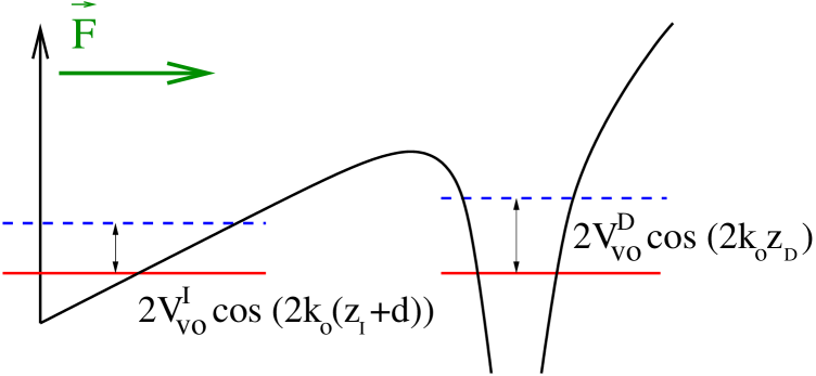
We consider a P donor in Si, a distance from a (001) oxide interface, under a uniform electric field perpendicular to it (see Fig. 1). The donor is at and the interface is at . The ground state of the electron at the donor is written Kohn and Luttinger (1955)
| (1) |
where are envelope functions. In the presence of an interface (which is considered to produce an infinite barrier at ), we take Calderón et al. (2007)
| (2) |
with and variational parameters, and a normalization constant. Here are the Si band edge Bloch states , with Å the lattice parameter. The reference site is irrelevant for the individual Bloch states, for which it only contributes with a phase. However, for the superposition state such as given in Eq. (1), it represents a common pinning site of the Bloch states which, for the ground state of an isolated donor in Si, is naturally chosen to be at the position of the donor .Kohn and Luttinger (1955)
At a (001) interface, the conduction band edge six-fold degeneracy is broken Sham and Nakayama (1979); Ando et al. (1982); Kane (2000) and the and valleys are meV lower in energy than the other four valleys. The lowest energy states at the interface are the symmetric and antisymmetric combinations of these two valleys
| (3) |
whose degeneracy is lifted by the abrupt interface valley-orbit coupling. Sham and Nakayama (1979) is the interface envelope function Calderón et al. (2007)
| (4) | |||||
with and variational parameters. In the case of an isolated well, the pinning site should be near the interface, where the envelope electronic density is maximum and the potential is most attractive. Here we take (namely, at the interface); as shown below, the exact location of is not relevant for our results, as long as it is near the interface, far away from the donor site.
This problem has been previously addressed in the single valley approach. Calderón et al. (2006, 2007) In order to investigate multivalley effects in the simplest approximation, we assume that the donor ground state only involves the and valleys:
| (5) |
and are the relevant components which couple more strongly to the interface lowest states, and the lowest ones in Si under tensile strain [namely, grown on relaxed Si1-xGex (001)]. Koiller et al. (2002b) The envelopes and are the same as obtained in the single-valley calculation where the values of the variational parameters , , , and were determined. The remaining parameters, and , are optimized variationally here.
The Hamiltonian of a donor electron close to a Si/SiO2 interface is, in rescaled atomic units nm and meV,
| (6) | |||||
where , , and , cm/kV, and the electric field is given in kV/cm. The last term describes valley-orbit effects, namely the coupling between different valleys due to the singular nature of both the donor and the interface potentials. These couplings are quantified by the parameters and , as described below.
In our two-valley formalism, the problem is restricted to the basis set of the lowest uncoupled donor and interface states, namely , , , , leading to the Hamiltonian matrix
| (7) |
where , , and are the same as the single valley matrix elements. The two additional parameters, the pinning positions and , are calculated variationally. The valley-orbit (VO) coupling parameter at the donor is known from the isolated donor spectrum (splitting within the 1S manifold): For a P donor it is meV. Grimmeiss et al. (1982); Koiller et al. (2002b) We use this value throughout. However, the VO coupling at the interface depends on the sample, and different values have been reported in the literature. Takashina et al. (2006) We take as a parameter varying from to meV. The negative sign is chosen in analogy with the VO coupling at the donor, but our main conclusions only depend on the absolute value of . For , the ground state is a symmetric combination of the and valleys. Full valley-orbit coupling (maximum splitting between the symmetric and antisymmetric combinations of the and valleys, given in Eq. (3), with the symmetric one as the ground state) corresponds to at the donor well and at the interface well. When , the two combinations are degenerate at the interface. This degeneracy is broken when . Note that the donor states, defined in Eq. 5, would also be degenerate if is such that .
We define the overlap matrix
| (8) |
where is the overlap between the interface and donor envelopes, which is a decreasing function of . The four eigenvalues and eigenstates () satisfy .
According to our model, meaningful calculations refer to electric field intensities for which the envelope function of the donor well ground state may be described by a single 1S-like function. As shown in calculations of the Stark effect of P in Si, Debernardi et al. (2006) higher donor excited states contribute to the ground state under fields above kV/cm. We thus restrict our studies to intermediate to long distances, namely , so that the characteristic fields (see Fig. 1) remain below kV/cm.
III Results
As discussed in previous studies, Calderón et al. (2007) the characteristic field above which the electronic ground state is at the interface, as well as the time required to ‘shuttle’ the electron from the donor to the interface, are determined by a level anticrossing process involving the electronic ground state. The tunneling time has been estimated from the gap at anticrossing, . We focus here in the study of and as a function of and of , the interface VO coupling parameter.
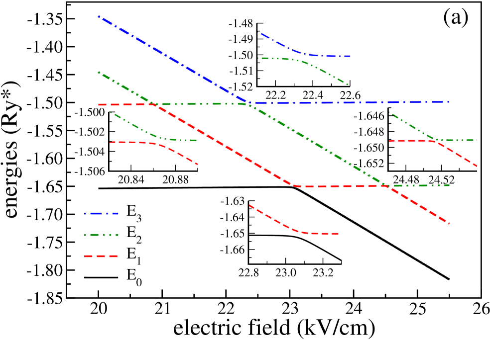
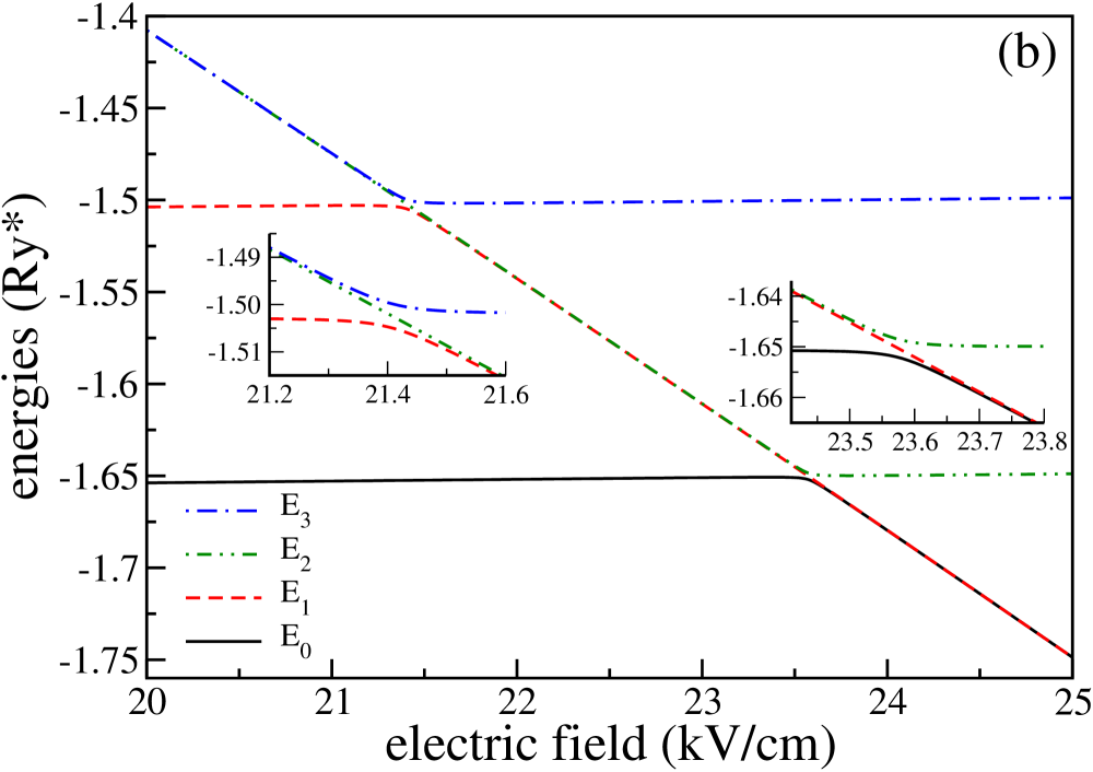
In Fig. 1 we illustrate the double well potential (donor plus interface) and the uncoupled two-valley levels (i.e., assuming ). In the single valley approximation, Calderón et al. (2007) the problem is two-dimensional, only two levels (one per well) are relevant and one anticrossing occurs at . In the present case, for , there are two non-degenerate levels in each well and, therefore, there are four level anticrossings as illustrated for meV and in Fig. 2 (a). The relevant anticrossing to determine and the gap is the one that involves the lowest eigenstate. When the interface states are doubly degenerate, namely , there are only two level anticrossings involving three levels each, see Fig. 2 (b). One of the levels at the anticrossing remains uncoupled to the other two that present the typical level repulsion with an associated gap. For meV, the results are sensitive to though the predominant behavior is similar to the degenerate case shown in Fig. 2 (b).
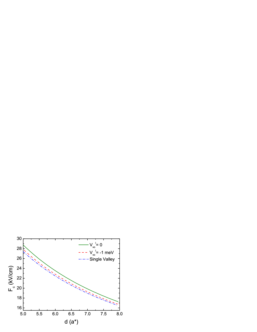
In Fig. 3 we compare the values of the characteristic field required to move the donor electron ground state from the donor to the interface within the single valley approximation and the 2-valley formalism for and meV. The behavior of obtained in the 2-valley formalism is qualitatively similar to the single valley approximation; only a small shift is obtained due to the different values of the ground state levels at each of the wells. The shift with respect to the single valley result is dependent on the relative values of and , being zero if . For a particular value of , decreases as increases.
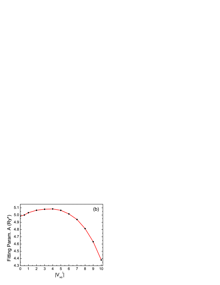
The smooth behavior of in the 2-valley formalism is not shared by the other quantity of interest: the gap at anticrossing (related to ’shuttling’ tunneling times). This is illustrated in Fig. 4 (a) where oscillations for the case meV are patent. The maxima of the gap oscillations correspond to tunneling times of the order of the single valley results Calderón et al. (2006) [see Fig. 4 (b)] while the gap minima would lead to much longer tunneling times. The periodicity of the oscillations is given by which is not commensurate with the lattice. Note that is not a continuous variable in a real system but its value changes in monolayer steps of Å. These values of correspond to the stars that sprinkle the continuous oscillating dashed line in Fig. 4 (a). Therefore, tunneling times are in practice undetermined (and could be much longer than predicted in the single valley approximation) unless the position of the donor is known with atomic precision. The gap amplitude (defined by a phenomenological fitting discussed in the figure caption) also depends on the value of as shown in Fig. 4 (b). Increasing leads to smaller gaps at anticrossing and therefore longer tunneling times (the difference between maximum and minimum times at a particular is ). In contrast, for , the gap decreases smoothly (with no oscillations) as increases.
The qualitatively distinct results obtained for and meV illustrated in Fig. 4 (a) emerges from the distinct level structures for these two cases, as shown in Fig. 2. For , the purely interface states are degenerate (high and low field limits in this figure). Under particular fields, this degeneracy is lifted because a specific superposition couples to a donor state, leading to an anti-crossing between these levels, while a second interface state remains uncoupled and unaffected. The relevant anticrossing in our studies does not involve the uncoupled state, which is never the lowest (or highest) energy state within the anticrossing range of fields. For , our numerical investigations show that for very small values of this parameter (e.g. meV) and for some values of , an interface level remains uncoupled and the gap behavior is very similar to the case. The oscillations in the gap appear consistently for all and meV.
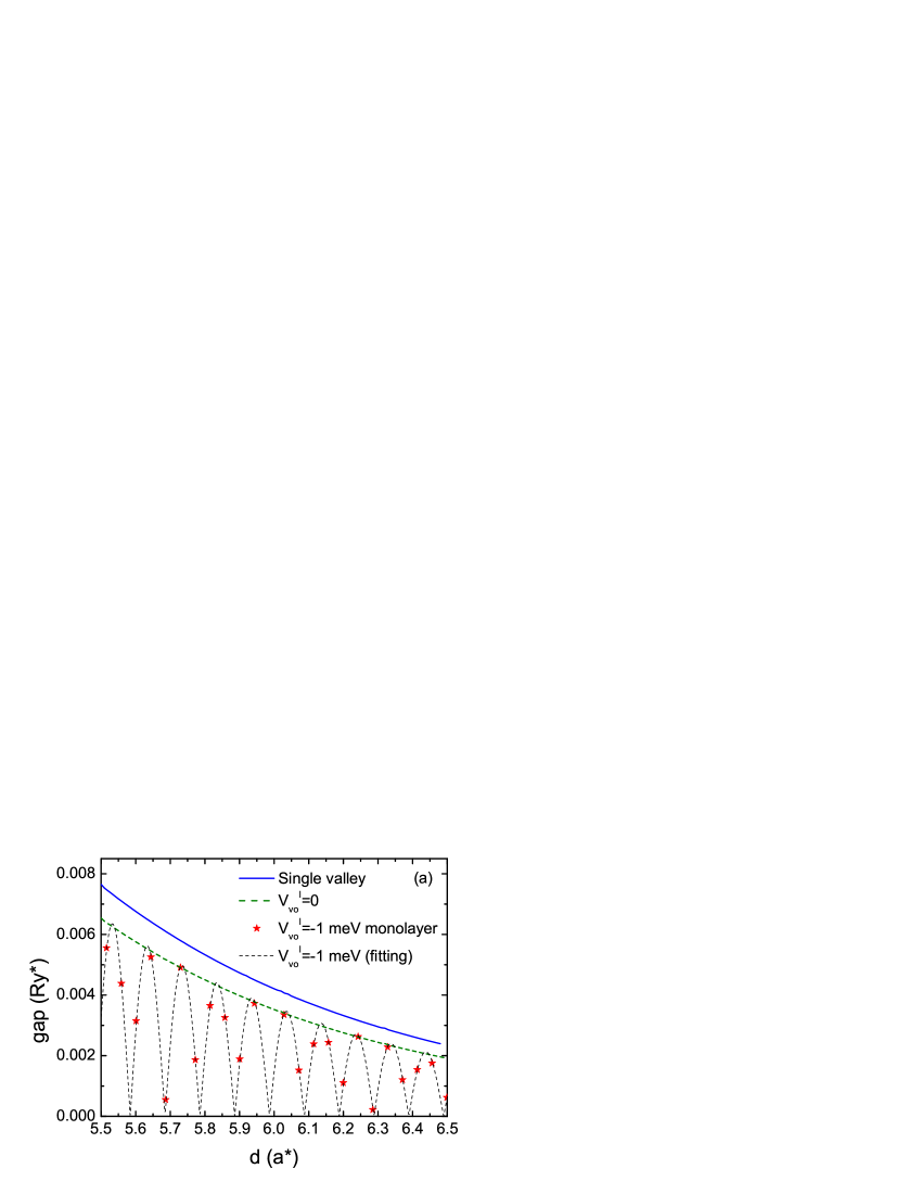
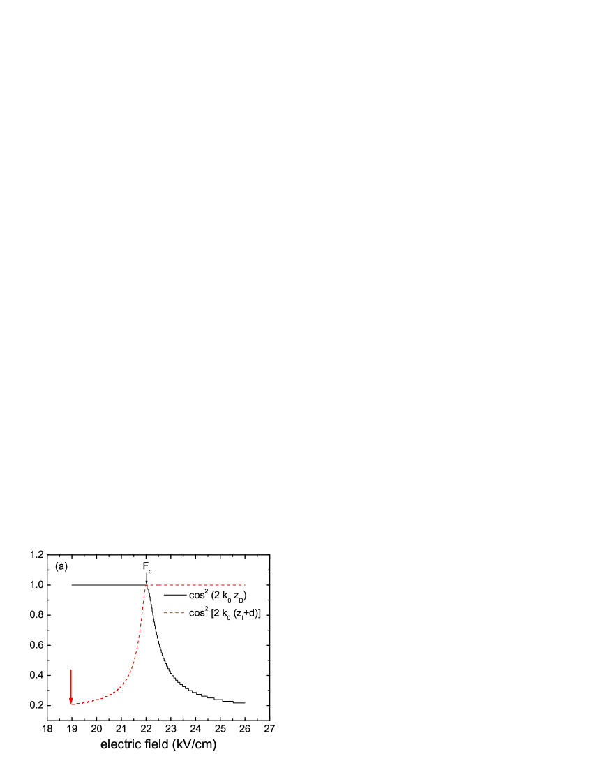
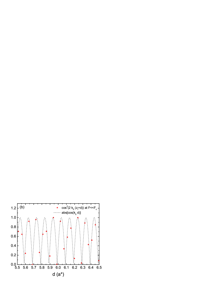
In Fig. 5 we show the values of the phase pinning sites and obtained variationally. The pinning sites depend on the applied electric field. Note that the splitting between the eigenstates in each of the wells depends on the cosines and (see Fig. 1). Therefore, in a generic case as the one depicted in Fig. 5 (a), the splitting between the two eigenstates (the symmetric and antisymmetric combinations of the and valleys) depends on . Importantly, the splitting is maximum [ or ] in the well where the electron ground state is (namely, at the donor for , and at the interface for ). The splitting in the well where the excited state is (the interface at and the donor at ) oscillates with between zero and maximum with the same periodicity as the gap, as shown in Fig. 5 (b). This implies that for the values of close to the minimum gap (), the eigenstates at the donor (interface) are almost degenerate for (). In these cases, the splitting switches from zero to its maximum possible value, and viceversa, at , with anticrossings involving the levels and producing a minimum gap. When corresponds exactly to degenerate states [], the gap is larger than the ones depicted in Fig. 4. However, due to the incommensurability of with respect to the lattice, the chance that satisfies is very small.
If and are fixed such that the related cosines are finite at all fields, the oscillations in the gap are preserved. The oscillations disappear when at least one of the wells has a degenerate ground state at all fields, and the problem reduces to the single valley approach if both VO couplings are zero.
IV Discussions and summary
It has been known for a few years that the exchange between electrons bound to donors separated by a distance oscillates with due to the interference between the valleys in the conduction band of Si. Koiller et al. (2002a); Andres et al. (1981) These oscillations present consequences for Si quantum computing if the 2-qubit operations rely on exchange coupling. Here we find that valley interference is also relevant for the quantum control and manipulation of single electrons in a donor/interface system. In particular, the tunneling times (or gaps) for the donor-interface shuttling have a periodic (non-commensurate with the lattice) dependence on the distance between donor and interface. These oscillations arise only when is non-zero ( is fixed to the bulk value of meV). For the qualitative behavior of the gap with reduces to that of the single valley approximation, namely, it shows no oscillations.
The oscillations in the gap versus can lead to very long tunneling times for donors at distances such that . In the current experiments, donors are ion implanted and form a doped layer with a distribution of distances with respect to the interface. Brown et al. (2006) In this case, our results would imply that some of those donors would never ionize in the relevant time scales, producing an effective reduction in the planar density of donors, a desirable feature in terms of allowing experiments to approach the single donor behavior. Calderón et al. (2006)
On the other hand, arbitrarily long tunneling times for donors at certain distances represent a serious overhead for the final objective of implementing a quantum computer using doped Si, as we need to be able to manipulate the electrons many times within the spin coherence time ( ms in bulk de Sousa and Das Sarma (2003); Witzel et al. (2005); Tyryshkin et al. (2006)). The disappearance of the oscillations when is of no help as a finite valley-orbit coupling is required for a well defined qubit, in particular, the valley-orbit splitting has to be larger than the spin splitting, which would determine the two states of a spin qubit. Fortunately, the statistical weight of the positions corresponding to vanishing gaps is relatively small (see the stars in Fig. 4 (a)) so most donors will be at positions at which the tunneling times are of the same order as the ones estimated within the single-valley approach. Calderón et al. (2006, 2007)
Experimentally, different values of have been reported depending on the quality of the interface and growing method. Takashina et al. (2006) This coupling can be a complex number. We have chosen to be negative and real and explored a wide range of values meV consistent with the ones reported. Takashina et al. (2006) We have also checked that, for , the gap versus amplitude is coincident with the case though its oscillations are shifted by half a period. We expect that a complex would give different shifts in the periodic function without affecting the gap amplitude and the decaying behavior (given by the fitting parameters and in Fig. 4).
In conclusion, we have analyzed the effect of the multivalley structure of the Si conduction band on the manipulation of electrons bound to donors close to a Si/SiO2 interface. Our results are based on a two-valley effective mass formalism, introduced here, and our main conclusions are expected to remain valid if the full multivalley degeneracy at the donor (with six valleys) were included. The characteristic field needed to shuttle an electron between the donor and the interface well is not qualitatively affected by valley-interference. The behavior of this quantity is in agreement with our previous single-valley treatment. Calderón et al. (2006) However, the tunneling times involved in the process oscillate with the distance between the donor and the interface at the atomic scale. The single-valley results typically give a lower bound for the tunneling times (upper bound for the anticrossing gaps). This behavior must be taken into consideration in the practical implementation of a doped Si quantum computer, as direct and full control over the operations discussed here may require positioning of donors within atomic precision.
Acknowledgements.
This work is supported by LPS and NSA. B.K. also acknowledges support from CNPq, FUJB, Millenium Institute on Nanotechnology - MCT, and FAPERJ. M.J.C. acknowledges support from Ramón y Cajal Program and MAT2006-03741 (MEC, Spain).References
- Shinada et al. (2005) T. Shinada, S. Okamoto, T. Kobayashi, and I. Ohdomari, Nature (London) 437, 1128 (2005).
- Kane (1998) B. E. Kane, Nature 393, 133 (1998).
- Vrijen et al. (2000) R. Vrijen, E. Yablonovitch, K. Wang, H.-W. Jiang, A. Balandin, V. Roychowdhury, T. Mor, and D. DiVincenzo, Phys. Rev. A 62, 012306 (2000).
- Skinner et al. (2003) A. J. Skinner, M. E. Davenport, and B. E. Kane, Phys. Rev. Lett. 90, 087901 (2003).
- Calderón et al. (2006) M. J. Calderón, B. Koiller, X. Hu, and S. Das Sarma, Phys. Rev. Lett. 96, 096802 (2006).
- Calderón et al. (2007) M. J. Calderón, B. Koiller, and S. Das Sarma, Phys. Rev. B 75, 125311 (2007).
- Martins et al. (2004) A. S. Martins, R. B. Capaz, and B. Koiller, Phys. Rev. B 69, 085320 (2004).
- Koiller et al. (2002a) B. Koiller, X. Hu, and S. Das Sarma, Phys. Rev. Lett, 88, 027903 (2002a).
- Takashina et al. (2006) K. Takashina, Y. Ono, A. Fujiwara, Y. Takahashi, and Y. Hirayama, Physical Review Letters 96, 236801 (2006).
- Kohn and Luttinger (1955) W. Kohn and J. M. Luttinger, Phys. Rev. 98, 915 (1955).
- Sham and Nakayama (1979) L. J. Sham and M. Nakayama, Phys. Rev. B 20, 734 (1979).
- Ando et al. (1982) T. Ando, A. B. Fowler, and F. Stern, Rev. Mod. Phys. 54, 437 (1982).
- Kane (2000) B. E. Kane, Fortschr. Phys. 48, 1023 (2000).
- Koiller et al. (2002b) B. Koiller, X. Hu, and S. Das Sarma, Phys. Rev. B 66, 115201 (2002b).
- Grimmeiss et al. (1982) H. G. Grimmeiss, E. Janzén, and K. Larsson, Phys. Rev. B 25, 2627 (1982).
- Debernardi et al. (2006) A. Debernardi, A. Baldereschi, and M. Fanciulli, Physical Review B 74, 035202 (2006).
- Andres et al. (1981) K. Andres, R. N. Bhatt, P. Goalwin, T. M. Rice, and R. E. Walstedt, Phys. Rev. B 24, 244 (1981).
- Brown et al. (2006) K. R. Brown, L. Sun, and B. Kane, Appl. Phys. Lett. 88, 213118 (2006).
- de Sousa and Das Sarma (2003) R. de Sousa and S. Das Sarma, Phys. Rev. B 68, 115322 (2003).
- Witzel et al. (2005) W. Witzel, R. de Sousa, and S. Das Sarma, Phys. Rev. B 72, 161306 (2005).
- Tyryshkin et al. (2006) A. M. Tyryshkin, J. J. L. Morton, S. C. Benjamin, A. Ardavan, G. A. D. Briggs, J. W. Ager, and S. A. Lyon, Journal of Physics: Condensed Matter 18, S783 (2006).