A planar multipole ion trap
Abstract
We report on the realisation of a chip-based multipole ion trap manufactured using micro-electromechanical systems (MEMS) technology. It provides ion confinement in an almost field-free volume between two planes of radiofrequency electrodes, deposited on glass substrates, which allows for optical access to the trap. An analytical model of the effective trapping potential is presented and compared with numerical calculations. Stable trapping of argon ions is achieved and a lifetime of 16 s is measured. Electrostatic charging of the chip surfaces is studied and found to agree with a numerical estimate.
pacs:
37.10.Ty,85.85.+j,41.90.+eI introduction
Microchip-based ion traps are being investigated in several laboratories worldwide for purposes ranging from mass spectrometry Blain et al. (2004); Shortt et al. (2005) to quantum information Seidelin et al. (2006); Pearson et al. (2006); Stick et al. (2006). Such traps can be precisely manufactured using micro-electromechanical systems (MEMS) technology offering highly integrated setups. Radiofrequency paul traps are being developed with ions trapped above the surface of a single chip Pearson et al. (2006); Seidelin et al. (2006) or between electrodes placed on different chips Schulz et al. (2006); M. Brownnutt, G. Wilpers, P. Gill, R. C. Thompson and A. G. Sinclair (2006). For loading these traps, photoionisation techniques using laser-ablated gas Hendricks et al. (2007) or laser-cooled neutral atoms Cetina et al. (2007) are utilized.
Here we present a planar microchip-based ion trap with a multipole arrangement of radiofrequency electrodes. Built from classically machined components, such multipole ion traps, in particular the 22-pole trap Gerlich (1995), are successfully used for the study of low-temperature ion-molecule reactions of astrophysical interest W. Paul, B. Lücke, S. Schlemmer and D. Gerlich (1995); Gerlich and Smith (2006) and to investigate laser-induced reaction processes Schlemmer et al. (2002); Asvany et al. (2005); Mikosch et al. (2004); Trippel et al. (2006); Dzhonson et al. (2007). The multipole structure leads to an effective potential with a finite depth and a large field-free central region Gerlich (1995); Trippel et al. (2006); Mikosch et al. (2007) that allows for buffer gas thermalization of the translational and rovibrational degrees of freedom of trapped molecular ions J. Glosík, P. Hlavenka, R. Plašil, F. Windisch, D. Gerlich, A. Wolf, and H. Kreckel (2006); S. R. Mercier, O. V. Boyarkin, A. Kamariotis, M. Guglielmi, I. Tavernelli, M. Cascella, U. Rothlisberger, and T. R. Rizzo (2006); Mikosch et al. (2004). We have transformed the cylindrical design of a conventional 22-pole trap into a planar electrode structure, which allows for MEMS fabrication. The open geometry of this planar configuration, and the application of transparent indium tin oxide (ITO) electrodes, will allow us to overlap an optically trapped cloud of ultracold atoms with ions confined in the microchip-based trap. This will open up opportunities for sympathetic cooling of ions with ultracold atoms and for experimental investigations of ultracold ion-atom interactions.
In this work, the operation of the planar trap and its characteristics are described. Numerical simulations of the trapping field and details of the MEMS process will be described elsewhere Kröner et al. . The paper is organized as follows: an analytical model of the effective potential of the chip-based multipole trap is presented in the next section, followed by a description of the trap setup in section III. Experimental results on ion trapping and on the achieved trap lifetimes are discussed in section IV. The analysis of surface charging effects are presented in section V.
II Properties of the chip-based multipole ion trap
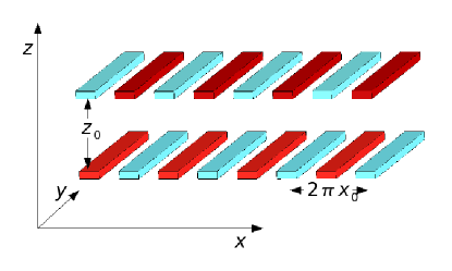
The basic components of the planar chip-based multipole ion trap are two sets of equally spaced and equally broad conducting stripes deposited on two insulating glass substrates that face each other. Fig. 1 shows a schematic view of the trap; every second stripe is connected to an rf-potential and the other stripes are connected to the opposing rf-potential . As shown below, this leads to a repulsive effective potential in front of each of the two electrode planes, thus yielding confinement of ions between the two planes. The distance from the center of one stripe to the center of the next one is given by and the distance between the two substrate surfaces is denoted . The width of the stripes is assumed to be . In our realisation mm and mm is employed.
For an analytical description of the potential generated by the two planes of radiofrequency electrodes we assume the plane to carry an infinite number of stripes and the stripes to extend infinitely in the plane. We further assume quasistationary conditions, a good approximation for trap frequencies in the MHz regime, and obtain the potential by solving the Laplace equation
| (1) |
Fig. 1 shows the employed coordinate system. The boundary conditions of the periodic arrangement of stripes are given by a periodic trapezoidal function: the potential is constant along the electrode surfaces and linear between the electrodes. This potential is approximated by the first order term of its Fourier series which reads . This approximate boundary condition satisfies the requirement of opposite voltages on neighbouring electrodes. For distances from the trap electrodes it is a good approximation, as shown below. For these boundary conditions an analytical solution for the electric field inside the trap is given by,
| (2) |
where and are reduced variables. The value of is linked to the potential applied to the electrodes by .
The effective potential that an adiabatically trapped ion experiences in a rapidly oscillating rf field is given by Gerlich (1992)
| (3) |
where the charge and mass of the ion are denoted as and . For the given solution for the chip-based ion trap this yields
| (4) |
For this solution is approximately proportional to . This is in contrast to cylindrical multipole ion traps of order , such as the 22-pole trap () Gerlich (1995), which feature effective potentials proportional to .
The necessary condition of adiabatic motion for a trapped ion in a time-varying field is characterized by the adiabaticity parameter Gerlich (1992)
| (5) |
Ref. Gerlich (1992) postulates that has to be less than 0.3 to guarantee “safe operating conditions”. We have thoroughly investigated trap loss out of multipole traps Mikosch et al. (2007) and found trapping to occur up to a value of 0.38 for . Where reaches this maximum value the surface of the trapping volume is reached. The effective potential on this surface represents the maximum potential depth for trapped ions Mikosch et al. (2007). The right panel of Fig. 2 shows the effective trapping potential of the chip-based multipole ion trap in the region of space where adiabatic trapping is possible, i. e. where the adiabaticity criterion of is fulfilled. The potential is calculated for Ar+ ions in a trap of amplitude V and frequency MHz. It can be seen that the effective potential is represented by a deep well with an almost flat, field-free bottom and with exponentially rising potential walls and a height of about 0.5 eV.
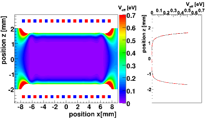
The electric field configuration for stable ion trapping has also been investigated in numerical simulations and the resulting effective trapping potentials and -parameters are evaluated Kröner et al. . From a two-dimensional simulation of the effective trapping potential using SIMION sim , a one-dimensional cut along the -direction in the center of the trap (for ) is derived. It cannot be distinguished from the analytical model in the right panel of Fig. 2. Both results are found to agree within one percent, which proves the applicability of the analytical model in the region of the trap where adiabatic motion prevails. The full two-dimensional calculation in the -plane is shown in the left panel of Fig. 2. We find that the confinement in the -direction is independent of the -position for almost the entire trap. One can also see that the confinement for small and large -values is not provided by the rf fields. The same holds for small and large -values. Confinement in the -plane is therefore achieved by superimposing additional electrostatic potentials.
III Realisation of the trap and loading scheme
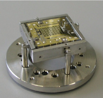
Two planes of gold electrodes on top of two glass substrates that face each other form the ion trap. Design and fabrication of the chip-based ion trap using MEMS technology will be described in a separate publication Kröner et al. . Fig. 3 shows a picture of one of the two glass substrates with the rf electrodes, spaced at mm, and several static electrodes surrounding the comb structure. Besides providing three-dimensional trapping these static electrodes are also used for the controlled extraction of trapped ions. The second glass chip is mounted facing the first one at a distance of mm.
The trap is kept in a vacuum chamber at a residual gas pressure of about generated by a turbo molecular pump. It is mounted in a holder fixed at one flange which also supports the electrical connections for the trap. The radiofrequency amplitude of the trap is generated by amplifying the signal of an rf oscillator (Hameg HM8032) in a high frequency power amplifier (RFPA RF001100-8). To reach sufficiently high amplitudes the output is transformed by a coil on a high frequency ferrite core located close to the trap outside the chamber. In this way peak amplitudes of V and frequencies in the range of MHz are applied.
Ions are created by electron impact on neutral atoms inside the trap. This is achieved by crossing a pulsed gas beam from a piezoelectric valve Person and Gerlich with a pulsed 1 kV electron beam in the center of the trap. Creating the ions inside the trap is favored over ion transport and capturing techniques due to its simplicity but causes charging of non conducting parts (see section V) as well as a higher background pressure for the first tenths of ms after the pulse. When ions are created the electron beam is adjusted by optimizing the ion signal on a channeltron detector, which is mounted opposite of the pulsed valve and is set up to detect and amplify individual ion pulses. The number of ions hitting the detector are measured using a single channel discriminator and a counter. Large numbers of trapped ions are measured by digitizing the current signal of the channeltron with an oscilloscope. The data acquisition timing is controlled with an AVR Atmel microprocessor (AT90S8515).
IV Characterization of the trap
Operation of the planar ion trap with Ar+ ions has been achieved with the design parameters for the rf and dc potentials obtained from the numerical simulations, i. e. MHz and V. The best operating conditions are found by optimizing the electrostatic electrodes surrounding the trap. These optimal settings result in static voltages of up to a few volts. The setup is found to be stable against slight variations of single static potentials: varying the static potentials by less than 1 Volt from their optimum values decreases the lifetime due to a lower potential depth, but trapping is still possible.
For extraction the potential of the surrounding border electrode in the direction of the detector is lowered to -15 V. More negative extraction potentials lead to a decrease in ion signal as the ions are hitting the electrode. More positive extraction potentials lead to a smearing of the ion signal in the time domain as the ions close to the border are accelerated by the extraction potential but the ions further away are much less influenced. In experiments with few trapped ions up to 200 individual ions are counted, limited by the overlapping ion signals in the counter. We use these data to calibrate the analog current signal of the channeltron detector to the ion number. In this way the largest observed analog signals of trapped ions are found to contain about 3000 ions.
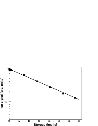
For the ion trap we determine a storage time of 16 s, which corresponds to a loss rate of 0.06 s-1. This lifetime can be compared to the evaporation limited lifetime over the rim of the trapping potential Mikosch et al. (2007): The evaporation rate is given by
| (6) |
where the trap depth V is taken from the effective potential calculation of section II. The temperature of the trapped ions is estimated to be roughly room temperature, controlled by collisions of the trapped ions with the gas injected into the trap chamber after ion formation. The pre-factor is assumed to be similar to the value obtained in the 22-pole ion trap, s-1 Mikosch et al. (2007). This yields a value of about 0.02 s-1, which is only a factor of three away from the measured storage time. This is considered a fair agreement when keeping in mind the exponential dependence of the evaporation rate on the trap depth .
V Electrostatic charging
Avoiding stray charges and investigating their effects where they can not be completely eliminated is a central issue in the design of micro trap structures where conducting and nonconducting areas are lying close to each other and to the center of the trap Seidelin et al. (2006). In our current trap design these charging effects are non-negligible and affect both trapping efficiency and storage time.
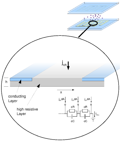
The steady-state potential of the glass surface induced by charging can be calculated assuming a constant current density that is flowing onto the surface and a resistivity-limited discharging current within the glass (see Fig. 5). The current inside the surface flows from the middle of the high-resistive region (denoted as ) to the two neighbouring electrode stripes. A surface area (with perpendicular to the stripes and parallel to the stripes) leads to a discharging current at the position inside the glass of
| (7) |
Under steady state conditions only the resistivity of the glass substrate and not the parallel capacity determines the potential (see equivalent circuit diagram in Fig. 5). This leads to a potential gradient at a position between the stripes of
| (8) |
where the discharching current flows through the area in the glass chip and denotes the specific resistance of the glass. Integration from to yields the electric potential at the center of the high-resistive region () of
| (9) |
with respect to the electrodes. For an estimation of the amount of charge needed to significantly influence storage of ions we assume that a potential of 500 mV between two rf electrodes, a value similar to the depth of the effective potential, will preclude trapping of ions. The resistivity of the glass substrate (thickness cm) is extrapolated from the material data sheet bor to . Thus, a potential of 500 mV is obtained for a charging current density of about electrons per cm2 and second. For the two entire chips with their total glass surface of cm2, this means that a charge flux of about elementary charges per second will have a significant influence on trapping and storage. At the typical repetition rate of the experiment of 10 cycles per second, this yields a maximum allowable current of charges per trap loading.
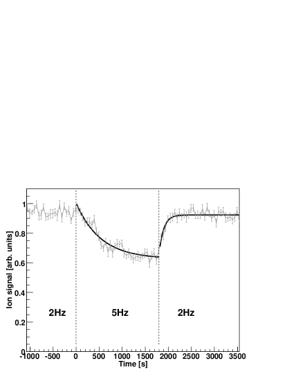
To investigate charging effects of the planar ion trap experimentally, the trapping efficiency is measured for different average currents of the electron beam used for ionization. We define the trapping efficieny as the number of ions trapped after 10 ms of storage time. This time is much shorter than the lifetime of trapped ions but is also long enough to allow for complete randomization of ion trajectories. In the experiment, charging of the chips’ surface stems from the electron beam, which is pulsed on only during loading of the trap. The average charging current can therefore be varied by changing the repetition rate of trap loading from 0.1 Hz to 20 Hz. The trapping efficiency is measured for many trapping cycles over a time span of several hours. In Fig. 6 the change in the trapping efficiency is shown when the repetition rate is changed from 2 Hz to 5 Hz and back to 2 Hz. With the higher repetition rate the charging increases and consequently the trapping efficiency decreases until the repetition rate is set back to 2 Hz and the charging is reduced again. The time constants for reaching steady-state trapping efficiencies upon increased and decreased surface charging are obtained by fitting a decay curve and a growth curve to the data (solid line in Fig. 6). The obtained values for increased and decreased charging amount to s and s, respectively. The observation of two different values may indicate that the increased charging is limited by the current whereas the decreased charging is only limited by the intrinsic capacitance and resitivity of the substrate.
To estimate the expected time constant for discharging the surface we use the equivalent circuit of the chip surface shown in Fig. 5. The time constant that determines changes of the steady-state potential depends on the resistance and the capacity . This yields the time constant
| (10) |
With for the glass substrate bor one obtains a typical time constant of about 400 s for changes of the charging potential of the glass substrate. Under the assumption that small changes of the trapping efficiency are to a first approximation proportional to small changes in the charging potential one can compare this calculated time constant to the values obtained from the measured trapping efficiency. The order of magnitude agreement that one finds provides evidence that charging of the glass surface is in fact the major cause for the observed changes in the trapping efficiency. Decreasing the resistivity of the glass substrate by an order of magnitude one can proportionally reduce the charging potentials of the substrate to an insignificant amount, while still maintaining small resistive losses for the driving rf amplitude.
VI Conclusions and outlook
We have presented a chip-based multipole ion trap based on a planar design, which features a large field free trapping volume between two glass substrates carrying stripes of radiofrequency electrodes. An analytical model has been presented that describes the effective trapping potential in good agreement with numerical calculations. Trapping of ions has been demonstrated and the measured decay rate of trapped Ar+ ions follows the expectations from evaporative losses over the rim of the confining potential. The effect of surface charging, due to the highly resistive glass substrates, on the ion trapping efficiency has been experimentally studied. The charging potential and the observed time constant for reaching steady-state conditions has been successfully modeled using an appropriate equivalent circuit, which is based on the resistivity and capacity of the glass substrate.
As a next step we will add a drift tube for the extracted ions to implement a Wiley McLaren Wiley and McLaren (1955) type time of flight mass spectrometer. To characterize the density distribution of the trapped ions, photodetachment tomography experiments Trippel et al. (2006) will be carried out. Further improvements of the design and the fabrication techniques of the trap are under development, including electrode materials with high optical transmission Kröner et al. . This will allow the combination of the chip-based multipole ion trap with a magneto optical trap for ultracold neutral atoms for experiments on interactions of trapped ions and clusters with ultracold atoms.
Acknowledgements.
This project is supported in part by a grant from the Ministry of Science, Research and Arts of Baden-Württemberg. The chips were fabricated in the Clean Room Service Center of the Department of Microsystems Engineering (IMTEK), Freiburg. N. M. acknowledges support from the RISE program of the German Academic Exchange Service (DAAD).References
- Blain et al. (2004) M. G. Blain, L. S. Riter, D. Cruz, D. E. Austin, G. Wu, W. R. Plass, and R. G. Cooks, Int. J. Mass Spectrom. 236, 91 (2004).
- Shortt et al. (2005) B. J. Shortt, M. R. Darrach, P. M. Holland, and A. Chutjian, J. Mass Spectrom. 40, 36 (2005).
- Seidelin et al. (2006) S. Seidelin, J. Chiaverini, J. J. Bollinger, D. Leibfried, J. Britton, J. H. Wesenberg, R. B. Blakestad, R. J. Epstein, D. B. Hume, W. M. Itano, et al., Phys. Rev. Lett. 96, 253003 (2006).
- Pearson et al. (2006) C. E. Pearson, D. R. Leibrandt, W. S. Bakr, W. J. Mallard, K. R. Brown, and I. L. Chuang, Phys. Rev. A 73, 032307 (2006).
- Stick et al. (2006) D. Stick, W. K. Hensinger, S. Olmschenk, M. J. Madseb, K. Schwab, and C. Monroe, Nature Physics 2, 36 (2006).
- Schulz et al. (2006) S. Schulz, U. Poschinger, K. Singer, and F. Schmidt-Kaler, Fortschr. Phys. 54, 648 (2006).
- M. Brownnutt, G. Wilpers, P. Gill, R. C. Thompson and A. G. Sinclair (2006) M. Brownnutt, G. Wilpers, P. Gill, R. C. Thompson and A. G. Sinclair, New Journal of Physics 8, 232 (2006).
- Hendricks et al. (2007) R. J. Hendricks, D. M. Grant, P. F. Herskind, A. Dantan, and M. Drewsen, Appl. Phys. B 88, 507 (2007).
- Cetina et al. (2007) M. Cetina, A. Grier, J. Campbell, I. Chuang, and V. Vuletic, Phys. Rev. A 76, 041401(R) (2007).
- Gerlich (1995) D. Gerlich, Phys. Scripta T59, 256 (1995).
- W. Paul, B. Lücke, S. Schlemmer and D. Gerlich (1995) W. Paul, B. Lücke, S. Schlemmer and D. Gerlich, Int. J. Mass Spectrom. Ion Proc. 149/150, 373 (1995).
- Gerlich and Smith (2006) D. Gerlich and M. Smith, Phys. Scripta 73, C25 (2006).
- Schlemmer et al. (2002) S. Schlemmer, E. Lescop, J. von Richthofen, D. Gerlich, and M. Smith, J. Chem. Phys. 117, 2068 (2002).
- Asvany et al. (2005) O. Asvany, P. K. P, B. Redlich, I. Hegemann, S. Schlemmer, and D. Marx, Science 309, 1219 (2005).
- Mikosch et al. (2004) J. Mikosch, H. Kreckel, R. Wester, R. Plasil, J. Glosik, D. Gerlich, D. Schwalm, and A. Wolf, J. Chem. Phys. 121, 11030 (2004).
- Trippel et al. (2006) S. Trippel, J. Mikosch, R. Berhane, R. Otto, M. Weidemüller, and R. Wester, Phys. Rev. Lett. 97, 193003 (2006).
- Dzhonson et al. (2007) A. Dzhonson, E. B. Jochnowitz, and J. P. Maier, J. Phys. Chem. A 111, 1887 (2007).
- Mikosch et al. (2007) J. Mikosch, U. Frühling, S. Trippel, D. Schwalm, M. Weidemüller, and R. Wester, Phys. Rev. Lett. 98, 223001 (2007).
- J. Glosík, P. Hlavenka, R. Plašil, F. Windisch, D. Gerlich, A. Wolf, and H. Kreckel (2006) J. Glosík, P. Hlavenka, R. Plašil, F. Windisch, D. Gerlich, A. Wolf, and H. Kreckel, Phil. Trans. R. Soc. A 364, 2931 (2006).
- S. R. Mercier, O. V. Boyarkin, A. Kamariotis, M. Guglielmi, I. Tavernelli, M. Cascella, U. Rothlisberger, and T. R. Rizzo (2006) S. R. Mercier, O. V. Boyarkin, A. Kamariotis, M. Guglielmi, I. Tavernelli, M. Cascella, U. Rothlisberger, and T. R. Rizzo, J. Am. Chem. Soc. 128, 16938 (2006).
- (21) M. Kröner, M. Debatin, J. Mikosch, S. Trippel, E. Just, M. Reetz-Lamour, R. Wester, M. Weidemüller, and P. Woias, in preparation.
- Gerlich (1992) D. Gerlich, Adv. Chem. Phys. 82, 1 (1992).
- (23) SIMION 7.0, Idaho National Engineering Laboratory.
- (24) U. Person and D. Gerlich, unpublished.
- (25) Borofloat 33, Product information and datasheet, Schott Glas, Mainz.
- Wiley and McLaren (1955) W. C. Wiley and I. H. McLaren, Rev. Sci. Instrum. 26, 1150 (1955).