Universal dynamical conductance in graphite
Abstract
We find experimentally that the optical sheet conductance of graphite per graphene layer is very close to , which is the theoretically expected value of dynamical conductance of isolated monolayer graphene. Our calculations within the Slonczewski-McClure-Weiss model explain well why the interplane hopping leaves the conductance of graphene sheets in graphite almost unchanged for photon energies between 0.1 and 0.6 eV, even though it significantly affects the band structure on the same energy scale. The f-sum rule analysis shows that the large increase of the Drude spectral weight as a function of temperature is at the expense of the removed low-energy optical spectral weight of transitions between hole and electron bands.
One of the most remarkable macroscopic manifestations of quantum mechanics is the appearance of a universal conductance , where is the elementary charge and is the Planck constant, in various physical phenomena. This value appears in the quantum Hall effect vonKlitzingPRL80 ; LaughlinPRB81 , in the superconductor-insulator transition in two dimensions JaegerPRB86 ; FisherPRL90 and in 1D ballistic transport ButtikerPRB85 ; vanWeesPRL88 ; WharamJPC88 . Notably, all of these observations were restricted so far to the DC transport. Monolayer graphene NovoselovScience04 ; GeimNM07 represents an interesting example, where the optical, or AC, conductance due to optical interband transitions is expected to be frequency independent and solely determined by the same universal value AndoJPSJ02 ; GusyninPRL06 ; FalkovskyEPJB07 in a broad range of photon energies:
| (1) |
(index ’1’ refers to the real part). Quite remarkably, does not depend on microscopic parameters that normally determine optical properties of materials. This is a consequence of the unusual low-energy electronic structure that resembles the dispersion of relativistic particles GeimNM07 . At energies considerably smaller than the bandwidth ( 2 eV), the dispersion of monolayer graphene features massless electron and hole conical bands formed by the orbitals (as shown in the inset of Fig.2c), where is the momentum of the Dirac point (there are two of them at the points K and K’ of the Brillouin zone) and m/s is the Fermi velocity. This type of dispersion is qualitatively different from more common quadratic massive bands, as has been most convincingly demonstrated by a field dependence of Landau levels NovoselovNature05 ; ZhangNature05 ; SadowskiPRL06 ; JiangPRL07 .
The absolute value of the optical conductance in graphene, the determination of which is an experimentally challenging task, has not yet been reported. However, it is legitimate to ask whether the predicted universality can already be observed in the conventional bulk graphite. Here we experimentally show that the answer is affirmative and explain it using the classical Slonczewski-Weiss-McClure (SWMcC) band model of graphite SWMcC .
It is instructive to begin with a short summary of expected optical properties of monolayer graphene. Eq.(1), apart from the numerical factor, follows from a simple dimensional analysis. When the chemical potential is zero, the conductance is given by the formula:
| (2) |
where is the velocity matrix element between the initial state with energy - and the final state with energy , is the 2D joint density of states and is the Fermi-Dirac distribution. If only the nearest neighbor hopping is present then and , where 1.42 Å is the interatomic distance and 3 eV is the hopping value. Therefore the non-universal parameters , as well as the frequency in equation (2) cancel and one obtains at zero temperature . An interesting consequence of equation (1) is that the optical transmittance of a free standing monolayer graphene sample is also frequency independent and is expressed solely via the fine structure constant :
| (3) |
as follows from the Fresnel equations in the thin-film limit. The calculated conductance of undoped graphene is shown in figure 2c for several temperatures RemarkCalculation . The depletion of the low-energy conductance with temperature is due to the gradual equilibration of the electron and hole occupation numbers close to the Fermi level. The ’removed’ optical spectral weight accumulates at zero frequency as a Drude peak (not shown), whose integrated intensity increases linearly with temperature PedersenPRB03 ; FalkovskyEPJB07 :
| (4) |

Optical measurements from 10 to 300 K were performed on highly ordered pyrolytic graphite (HOPG) of ZYA grade with a c-axis misorientation smaller than 0.4∘. Samples were cleaved right before being inserted into a cryostat. Reflectivity at near-normal incidence was measured from 2 meV to 0.8 eV using a Fourier transform spectrometer (Fig. 1). The absolute value was obtained by in-situ gold evaporation. Our reflectivity spectra are in agreement with previous measurements TaftPR65 ; GuizzettiPRL73 ; LiPRB06 . In the range 0.7 - 4.5 eV, we extracted the real and the imaginary parts of the dielectric function from ellipsometric measurements (shown in the inset). The correction for the admixture of the interplane optical component to the ellipsometry spectra was initially performed using the c-axis dielectric function found in Ref. GreenawayPR69 and refined by comparing the reflectivity and ellipsometric spectra in the range where they overlap. The uncertainty due to this procedure is the main source of the error bar shown in figure 2a. The complex in-plane conductivity in the whole range was derived using a Kramers-Kronig consistent procedure KuzmenkoRSI05 , where the phase of the complex reflectivity at low energies is anchored by ellipsometric data. The sheet conductance per graphene layer was calculated using the relation , where = 3.35 Å is the interlayer distance. Importantly, the optical measurements reflect mostly bulk material properties, since the penetration depth is several tens of .
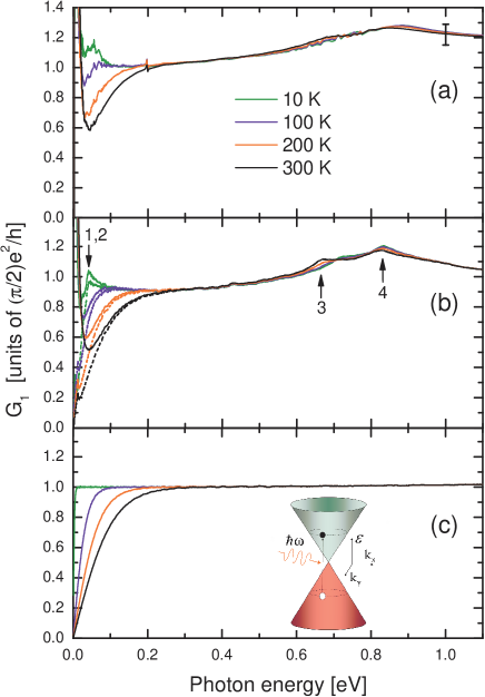
Figure 2a shows the real part of the measured conductance of HOPG normalized by . One can notice a remarkable similarity between these spectra and the calculated ones for graphene (panel c). The conductance is almost constant and close to , especially between 0.1 and 0.6 eV. The second observation is that the conductance at low energies shows a strong depletion with increasing temperature in a fashion very similar to the temperature dependence of in graphene. In contrast to the graphene spectra, the conductance of graphite shows a Drude peak below 10-20 meV, an extra structure at about 50 meV and two broad peaks at about 0.7 and 0.9 eV. The small narrow peak at 0.2 eV is an optical phonon BrillsonJPCS71 . In general, we conclude that the universality of the conductance envisaged for the isolated graphene is also present graphite in a broad energy range, in spite of the modification of the band structure by a significant c-axis hopping ( 0.3 eV) SWMcC . This result is not trivial since the universal conductance is observed at energies of the order of . For example, the calculated sheet conductance of bilayer graphene shows a strong frequency dependence caused by the interlayer hopping NilssonPRL06 ; AbergelPRB07 .
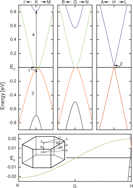
In order to understand this observation, we calculated infrared spectra of graphite with the standard AB stacking using a tight-binding Hamiltonian, which contains all hopping terms of the SWMcC model SWMcC and the on-site energy difference between the non-equivalent carbon atoms. The particular values of parameters, which were assumed to be temperature independent, were taken from Ref. PartoensPRB06 . The optical conductivity due to the direct interband transitions and the Drude (intraband) spectral weight were obtained using the standard relations, taking the temperature dependent occupation numbers into account. The integration was performed with an increased density of points near the K-H line along which the small Fermi surface is stretched, in order to improve the energy resolution at low frequencies. The four tight-binding bands of graphite in the vicinity of the K-H line are presented in figure 3. Near the H point, the bands are conical, as in monolayer graphene, while they acquire a small mass, of the order of 5 percent of the free electron mass, as in double-layer graphene as one moves towards the K point. The two bands depicted in black and blue disperse strongly along the c-axis (by about 1.5 eV), while for the other two bands (red and green) the dispersion is only 40 meV. This latter dispersion is responsible for the fact that the Fermi surface is electron like at the K point and hole like at the H point. Overall, this picture is in agreement with the recent ARPES ZhouNP06 ; GruneisCM07 and de Haas-van Alphen LukyanchukPRL04 measurements.
The in-plane conductance of graphite computed for this band structure is shown in figure 2b. One can see that the simple band calculation is sufficient to understand the survival of the universal conductance value in the mid-infrared range. There are two important factors that favor this. First, the energy of the Dirac point varies only weakly along the K-H line. We note that in doped graphene () the conductance is gapped below GusyninPRL06 . The position of the Dirac energy with respect to the chemical potential changes from about -20 meV at the H point to about 20 meV at the K point, which explains why the interband conductance precipitates dramatically below 40 meV (at =0) and forms a peak-like structure marked by 1 and 2. Importantly, this energy scale strongly depends on the type of stacking. For example, a similar calculation on a hypothetical AA-stacked graphene (not shown here) indicates that in this system the conductance would be strongly suppressed below 1.5 eV.
The second factor is a less obvious but an equally essential one. The frequency-independent conductance can be easily explained only in the case of non-split conical bands, while in graphite the bands are split and slightly parabolic, except close to the H point. In fact, a partial conductance (not shown) calculated for all momentum states with a certain value of away of the H point has a strong frequency dependence, very similar to the expected conductance of bilayer graphene NilssonPRL06 ; AbergelPRB07 . It shows a sharp double peak due to the transitions marked as 3 and 4 and a depletion at lower energies where only two bands out of four contribute to it. Essentially, the optical weight is redistributed by the c-axis hopping. However, in the total (i.e. the integrated) conductance this redistribution is almost averaged out, due to the fact that the splitting size changes continuously from the maximum value (0.7 eV for the transition 3 and 0.9 eV for the transition 4) at the K point to zero at the H point. Only close to the K point, where the bands show a van Hove singularity, these transitions make two broad conductance peaks 3 and 4 TaftPR65 ; GuizzettiPRL73 .
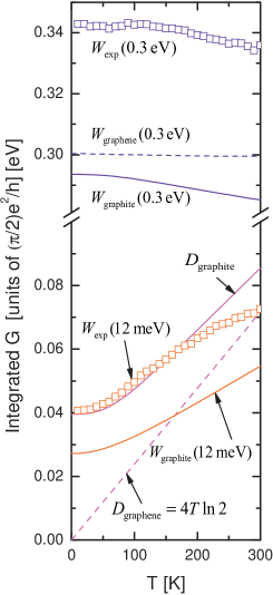
Finally, we study the redistribution of the optical spectral weight between different energy regions using the f-sum rule analysis. The red and the blue symbols in figure 4 show the measured temperature dependence of the low-energy integrated conductance for = 12 meV and 0.3 eV respectively. The first one consists mostly of the Drude (intraband) spectral weight which strongly increases as a function of temperature due to the thermally excited electron-hole pairs. The second one contains both the Drude weight and the low-energy transitions between the hole and electron bands. The fact that it is practically independent of temperature proves that the Drude spectral weight is at the expense of the suppression of the low-lying interband conductance. The observed temperature dependence agrees nicely with the described above calculations in graphite (solid lines). The absolute experimental values are somewhat higher than the theory predicts, which might be due to some underestimation of the Drude weight by the SWMcC model with the particular values of the hopping parameters used as well as due to the absolute experimental uncertainty of . For the purpose of illustration, we show on the same graph the calculated pure Drude spectral weight of graphene (described by equation 4) and of graphite, although it would not be trivial to extract this exact value from the experimental data, due to an overlap between the Drude peak and the interband transitions. One can see, however, that the calculated temperature dependence of in graphite reflects well the one of the Drude weight alone.
In conclusion, our study reveals remarkable similarities between the measured optical conductance of highly ordered pyrolytic graphite per graphene layer and theoretical predictions for the monolayer graphene. First, the optical conductance of graphite due to the transitions between hole and electron bands is very close to the universal value of between 0.1 and 0.6 eV. Second, the optical spectral weight removed from the low-energy interband conductance at finite temperatures is transferred to the Drude peak. This implies that the low-energy charge dynamics in graphite is rather non-trivial as it involves simultaneously the Drude component and the transitions between the hole and electron bands. This work was supported by the Swiss National Science Foundation through the National Center of Competence in Research Materials with Novel Electronic Properties-MaNEP . We thank N.P. Armitage, D.N. Basov and Y. Kopelevich for useful discussions.
References
- (1) K. von Klitzing, G. Dorda and M. Pepper, Phys. Rev. Lett. 45, 494 (1980).
- (2) R.B. Laughlin, Phys. Rev. B. 23, 5632 (1981).
- (3) H. M. Jaeger et al., Phys. Rev. B 34, 4920 (1986).
- (4) M.P.A. Fisher,G. Grinstein and S.M. Girvin, Phys. Rev. Lett. 64, 587 (1990).
- (5) M. Buttiker et al., Phys. Rev. B 31, 6207 (1985).
- (6) B. J. van Wees et al., Phys. Rev. Lett. 60, 848 (1988).
- (7) D. A. Wharam et al., J. Phys. C 21, L209 (1988).
- (8) K.S. Novoselov et al., Science 306, 666 (2004).
- (9) A.K. Geim and K.S. Novoselov, Nature Materials 6, 183 (2007).
- (10) T. Ando, Y. Zheng and H. Suzuura, J. Phys. Soc. Japan, 71, 1318 (2002).
- (11) V. P. Gusynin, S. G. Sharapov and J. P. Carbotte Phys. Rev. Lett. 96, 256802 (2006).
- (12) L.A. Falkovsky and A.A. Varlamov, Eur. Phys. J. B 56, 281 (2007).
- (13) K.S. Novoselov et al., Nature 438, 197 (2005).
- (14) Y. Zhang et al., Nature 438, 201 (2005).
- (15) M. L. Sadowski et al., Phys. Rev. Lett. 97, 266405 (2006).
- (16) Z. Jiang et al., Phys. Rev. Lett. 98, 197403 (2007).
- (17) J.W. McClure, Phys. Rev. 108, 612 (1957); J.C. Slonzcewski and P.R. Weiss, Phys. Rev. 109, 272 (1958).
- (18) The calculations for monolayer graphene, shown in Fig.2c and 4, take the finite bandwidth in account. However, in the shown frequency range, almost coincides with , which is the result for perfectly conical bands.
- (19) T.G. Pedersen, Phys. Rev. B 67, 113106 (2003).
- (20) E.A. Taft and H.R. Philipp, Phys. Rev. 138, 197 (1965).
- (21) G. Guizzetti et al., Phys. Rev. Lett. 31, 154 (1973).
- (22) Z.Q. Li et al., Phys. Rev. B 74, 195404 (2006). The curves of shown in Fig. 1 of this Ref. were derived incorrectly from the reflectivity spectra as will be detailed in the forthcoming publication (Z.Q. Li and D.N. Basov, private communication).
- (23) D.L. Greenaway et al., Phys. Rev. 178, 1340 (1969).
- (24) A.B. Kuzmenko, Rev. Sci. Instrum. 76, 083108 (2005).
- (25) L.J. Brillson et al., in Physics of Semimetals and Narrow-Gap Semiconductors, edited by D.L. Carter and R.T. Bate (Pergamon, New York, 1971).
- (26) D.S.L. Abergel and V. Fal’ko, Phys. Rev. B 75, 155430 (2007).
- (27) J. Nilsson et al., Phys. Rev. Lett. 97, 266801 (2006).
- (28) B. Partoens and F.M. Peeters, Phys. Rev. B 74, 075404 (2006).
- (29) S.Y. Zhou et al., Nature Physics 2, 595 (2007).
- (30) A. Grüneis et al., cond-mat/0704.2682.
- (31) I.A. Lukyanchuk and Y. Kopelevich, Phys. Rev. Lett. 93, 166402 (2004).