Tunneling conductance in - and -wave superconductor-graphene junctions: Extended Blonder-Tinkham-Klapwijk formalism
Abstract
We investigate the conductance spectra of a normal/superconductor graphene junction using the extended Blonder-Tinkham-Klapwijk formalism, considering pairing potentials that are both conventional (isotropic -wave) and unconventional (anisotropic -wave). In particular, we study the full crossover from normal to specular Andreev reflection without restricting ourselves to special limits and approximations, thus expanding results obtained in previous work. In addition, we investigate in detail how the conductance spectra are affected if it is possible to induce an unconventional pairing symmetry in graphene, for instance a -wave order parameter. We also discuss the recently reported conductance-oscillations that take place in normal/superconductor graphene junctions, providing both analytical and numerical results.
pacs:
74.45.+c, 74.78.NaI Introduction
A key issue in understanding low-energy quantum transport at the interface of a non-superconducting and superconducting material, e.g. a normal/superconductor (N/S) interface, is the process of Andreev reflection. Although the existence of a gap in the energy spectrum of a superconductor implies that no quasiparticle states may persist inside the superconductor for energies below that gap, physical transport of charge and spin is still possible at a N/S interface in this energy-regime if the incoming electron is reflected as a hole with opposite charge. The remaining charge is transferred to the superconductor in the form of a Cooper pair at Fermi level. The study of Andreev reflection and its signatures in experimentally observable quantities such as single-particle tunneling and the Josephson current has a long history (see e.g. Ref. deutscher, and references therein). Only recently, however, has this field of research been the subject of investigation in graphene N/S interfaces beenakker ; beenakkerreview .
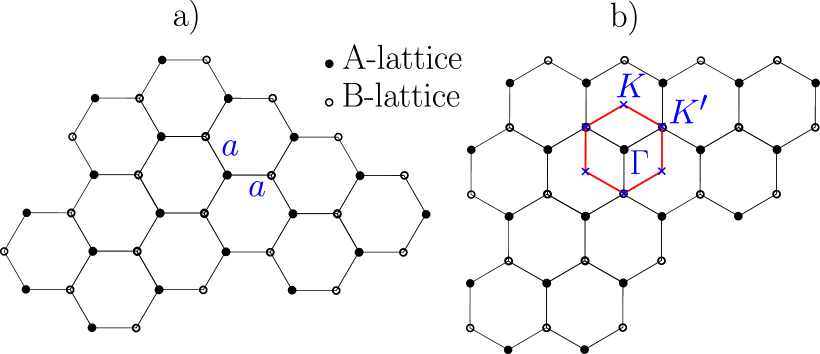
Graphene is a monoatomic layer of graphite with a honeycomb lattice structure, as shown in Fig. 1, and its recent experimental fabrication novoselov ; zhang has triggered a huge response in both the theoretical and experimental community over the last two years. The electronic properties of graphene display several intriguing features, such as the six-point Fermi surface and a Dirac-like energy dispersion, effectively leading to an energy-independent velocity and zero effective mass at the Fermi level. This obviously attracts the interest of the theorist, but graphene may also hold potential for technological applications due to its unique combination of a very robust carbon-based structural texture and its peculiar electronic features.
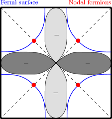
Condensed matter systems with such ‘relativistic’ electronic structure properties as graphene constitute fascinating examples of low-energy emergent symmetries; in this case, Lorentz-invariance. At half-filling, the Fermi level of graphene is exactly zero which renders the Fermi surface to be reduced to a six single points due to the linear intersection of the energy bands (see Fig. 3 and 4). The linear dispersion relation is a decent approximation even for Fermi levels as high as 1 eV, such that the fermions in graphene behave like they are massless in the low-energy regime. The fact that the fermions around Fermi level obey a Dirac-like equation at half-filling introduces Lorentz-invariance as an emergent symmetry in the low-energy sector. Another example where Lorentz-invariance appears for low-energy excitations is in one-dimensional interacting fermion systems, where phenomena like breakdown of Fermi-liquid theory and spin-charge separation take place. When Lorentz-invariance emerges in the low-energy sector of higher-dimensional condensed matter systems, it is bound to attract much interest from a fundamental physics point of view. Another interesting feature of graphene are the nodal fermions that are present at the Fermi level at half-filling. When moving away from half-filling by doping, the excitations at the Fermi level are no longer nodal. The nodal fermions of graphene hold certain similarities to, but also important differences from, the nodal Dirac fermions appearing in the low-energy sector of the pseudogap phase of -wave superconductors such as the high- cuprates. In contrast to graphene, the nodal fermions in the high- cuprates track the Fermi level when these systems are doped and thus represent a more robust feature than in graphene. For an illustration of the latter scenario, consider Fig. 2 which contains a sketch of the Fermi surface in the cuprates when including terms up to next-nearest neighbor hopping. The nodal lines of the -gap intersect the Fermi surface at exactly four points, which permits the existence of nodal fermions at those points in -space. However, in contrast to graphene, doping the system will in this case simply move the position of the Fermi arc with respect to the nodal line of the superconducting gap, such that the nodal fermions persist in the system QED3 . Nonetheless, the existence of the Dirac cones in graphene represents an important example of emergent non-trivial symmetries at long distances and low energies in higher (more than one) dimensional systems.
Although superconductivity does not appear intrinsically in graphene, it may be induced by means of the proximity effect by placing a superconducting metal electrode near a graphene layer heersche ; kasumov ; morpurgo ; buitelaar ; jariloo . Recent theoretical work beenakker ; sengupta have considered coherent quantum transport in N/S and normal/insulator/superconductor (N/I/S) graphene junctions in the case where the pairing potential is isotropic, i.e. -wave superconductivity. However, the hexagonal symmetry of the graphene lattice permits, in principle, for unconventional order parameters such as -wave or -wave (characterized by a non-zero angular momentum of the Cooper pair). A complete classification of the possible pairing symmetries on a hexagonal lattice up to -wave pairing () was given by Mazin and Johannes mazinjohannes , with the result given in Tab. 1. We underline that the notation ”insulator” in this context refers to a normal segment of graphene in which one experimentally induces an effective potential barrier . As we shall see, such a potential barrier has dramatically different impact upon the transport properties in graphene as compared to the metallic counterpart.
| Pairing | Type | Pairing | Type |
|---|---|---|---|
| 1 | |||
The intrinsic spin-orbit coupling in graphene is very weak, as dictated by the low value of the carbon atomic number, such that we will neglect it in this work. We will also disregard the electrostatic repulsion as mediated by the vector potential . At first sight, this might seem as an unphysical oversimplification since there is no metallic screening of the Coulomb interaction in graphene. In an ordinary metal, the renormalized Coulomb-potential reads , where is the Thomas-Fermi screening length and is the density of states (DOS) at Fermi level. Since pure graphene has zero DOS at Fermi level, one might quite reasonably suspect that the screening of charge vanishes, and it might seem paradoxical that Coulomb interactions can be neglected. The resolution to this is found by realizing that one may disregard the Coulomb interaction if it is weak compared to the kinetic energy in the problem. Due to the linear dispersion, the kinetic energy is governed by the Fermi velocity which formally diverges near Fermi level. The divergence is logarithmic and precisely due to the Coulomb interaction gonzales1999 ; kane2004 . The limiting velocity in graphene (due to e.g. Umklapp processes) is nevertheless of order m/s, see e.g. Ref. novoselov_nature, . This is roughly 100 times larger than in a normal metal, and it is thus safe to neglect the Coulomb interaction compared to the kinetic energy in graphene. In graphene, the Coulomb interaction self-destructs.
In this work, we will study in detail how an anisotropic order parameter induced in graphene will affect quantum transport in a N/S and N/I/S junction, extending the result of Ref. linderPRL07, . In equivalent metallic junctions, it is well-known hu that the zero bias conductance peak (ZBCP) is an experimental signature of anisotropic superconductivity in clean superconductors with nodes in the gap. This is a consequence of bound surface states with zero energy at the interface that form due to a constructive phase-interference between electron-like and hole-like transmissions into the superconductor tanaka . In graphene junctions with superconductors, as we shall see, a new phenomenology comes into play with regard to the scattering processes that take place at the N/S interface. It is therefore desirable to clarify how anisotropic superconductivity is manifested in the conductance spectra of such a junction, and in particular if the same condition for formation of a ZBCP holds for graphene junctions as well. As first shown in Ref. linderPRL07, , we will demonstrate that in N/I/S graphene junctions, novel conductance-oscillations as a function of bias voltage are present both for -wave and -wave symmetry of the superconducting condensate due to the presence of low-energy ‘relativistic’ nodal fermions on the N-side. The period of the oscillations decreases with increasing width of the insulating region, and persists even if the Fermi energy in I is strongly shifted. This contrasts sharply with metallic N/I/S junctions, where the presence of a potential barrier causes the transmittance of the junction to go to zero with increasing . The feature of conductance-oscillations is thus unique to N/I/S junctions with low-energy Dirac-fermion excitations. Moreover, we contrast the N/S or N/I/S conductance spectra for the cases where -wave and -wave superconductor constitutes the S-side. The former has no nodes in the gap and lacks Andreev bound states. The latter has line-nodes that always cross the Fermi surface in the gap, and thus features in addition to Andreev bound states, also nodal relativistic low-energy Dirac fermions. The quantum transport properties in a heterostructure of two such widely disparate systems, both featuring a particular intriguing emergent low-energy symmetry, is of considerable importance.
This paper is organized as follows. In Sec. II, we establish the theoretical framework which we shall adopt in our treatment of the N/S graphene junction. The results are given in Sec. III, where we in particular treat the role of the barrier strength and doping with respect to how the conductance is influenced by these quantities. In addition, we investigate the role of a possible unconventional pairing symmetry induced in graphene. A discussion of our findings is given in Sec. V, and we summarize in Sec. VI. We will use for matrices, and for matrices, with boldface notation for three-dimensional row vectors.
II Theoretical formulation
II.1 General considerations
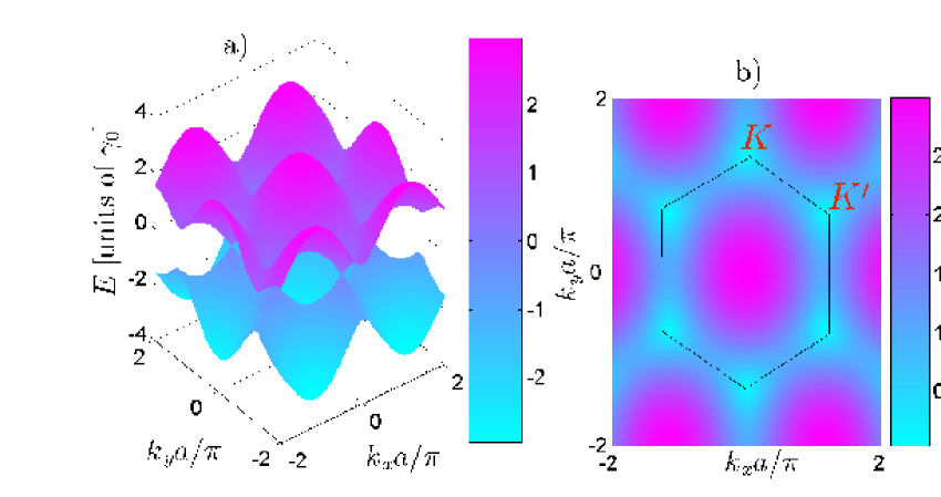
The Brillouin zone of graphene is hexagonal and the energy bands touch the Fermi level at the edges of this zone, amounting to six discrete points. Out of these, only two are inequivalent, which are conventionally dubbed and , and referred to as Dirac points. The band dispersion of graphene was first calculated by Wallace wallace , and reads
| (1) |
where eV, and the sign refers to the anti-bonding/bonding -orbital. The remaining three valence electrons are in hybridized -bonds. The energy dispersion in the Brillouin zone is plotted in Fig. 3, which reveals the conical structure of the conduction and valence bands at the six Fermi points. The cosine-like conduction and valence bands are made up by a mixture of the energy bands from the A- and B-sublattices in graphene (Fig. 1), which are linear near the Fermi level. This gives rise to the conical energy dispersion at the Dirac points and .
In order to introduce the new phenomenology of scattering processes in N/S graphene junctions, it is instructive to compare it with the metallic N/S junction. This is done in Fig. 4. In the metallic case, an incident electron with energy measured from the Fermi energy can not transmitted into the superconductor since there are no available quasiparticle states. Instead, it is reflected as a hole, represented as a quasiparticle with energy in the hole-like band, such that the leftover charge is transferred into the superconductor as a Cooper pair at Fermi level. The hole has negative mass, energy, wave-vector, and charge compared to the electron which is absent. Strictly speaking, only at are the wave-vectors exactly related through since one in general has
| (2) |
At finite energies, the electron-hole coherence will therefore be lost after the hole has propagated a distance
. At energies above the gap, Andreev reflection is severly suppressed since direct tunneling
into quasiparticle states is now possible.
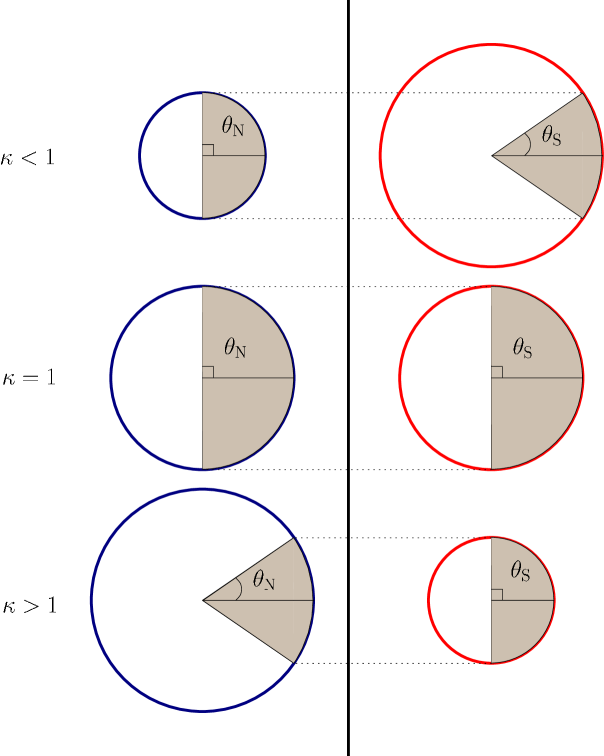
In graphene, a new phenomenology of Andreev reflection is at hand due to the band structure which effectively looks like that of a zero-gap semiconductor (see also Ref. beenakkerreview, ). Since the conduction and valence bands touch at the Fermi energy , one may distinguish between three important cases: i) undoped graphene with , ii) doped graphene with , and iii) heavily doped graphene with . These different scenarios are shown in Fig. 4.
In undoped graphene, with , an incident electron with energy is denied access as a quasiparticle into the superconductor, and physical transport across the junction is thus manifested through reflection as a hole. When Andreev reflection takes place, the transmitted Cooper pair is located at the Fermi level of the superconductor.
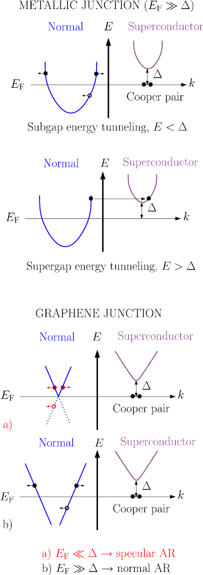
Energy conservation then demands that the missing electron in the normal region that is reflected as a hole must be located at due to the energy conservation, i.e. in the valence band. This is
different from normal Andreev reflection, since in that case both the electron and hole belong to the same band (conduction).
For specular Andreev reflection, however, they belong to different bands. The use of the term ”specular”
in order to characterize this type of Andreev reflection originates with the fact that the group velocity and momentum have the same sign for a valence band hole, while in contrast and have opposite signs for a conduction band hole. To see this, consider first a usual metallic parabolic dispersion for the electrons, such that one readily infers from
that . Therefore, a hole created at a given energy will have , since holes have
opposite group velocities of the electrons for a given wave-vector . For normal Andreev reflection, the
holes are located in the conduction band and therefore satisfy .
In the case of specular Andreev reflection for undoped graphene , a hole is generated in the valence band. Since in the valence band, the electronic dispersion reads , the group velocity of electrons is opposite to their momentum. Conversely, the group velocity for valence holes is parallell to their momentum. This is the mechanism behind specular Andreev reflection. In doped graphene (), the Andreev reflection can be normal or specular, depending on the energy of the incoming electron, as sketched in Fig. 4. In heavily doped graphene, (, only normal Andreev reflection is present for subgap energies since the distance from Fermi level to the valence band is too large for specular AR to occur. In the regime [0,], one has either normal or specular Andreev reflection, depending on the incident electron energy .
We also comment on the effect of Fermi vector mismatch (FVM). Blonder and Tinkham bt showed that in a metallic N/S junction, a FVM would act as a source for normal reflection, such that one could effectively account for it simply by choosing a higher value for the barrier strength . Interestingly, in a ferromagnet/superconductor junction the effect of a FVM could not be reproduced by simply shifting to a higher value, as discussed by Zutic and Valls zutic . In the absence of an exchange energy, however, the effect of FVM can be thought of as a reduction of the Fermi surface that participates in the scattering processes, as illustrated in Fig. 5. One may parametrize the FVM by the parameter where () is the Fermi momentum in the normal (superconducting) part of the system. In particular, it is seen that for , there is only possible transmission of quasiparticles (although these decay exponentially) up to a critical angle less than kashiwaya96 .
Having established the states that participate in the scattering at the interface, we now turn to equations that describe these quasiparticle states.
II.2 Scattering processes
Consider the case of zero external magnetic field. The full Bogoliubov-de Gennes (BdG) equation for the 2D sheet graphene normal/-wave superconductor junction in the -plane then reads beenakker ; beenakkerreview
| (3) |
where is the excitation energy, and denoting the electron-like and hole-like exictations described by the wave-function. Assuming that the superconducting region is located at and neglecting the decay of the order parameter in the vicinity of the interface bruder , we may write for the spin-singlet order parameter
| (4) |
where is the Heaviside step function, is the phase corresponding the globally broken symmetry in the superconductor, while is the angle on the Fermi surface in reciprocal space (we have adopted the weak-coupling approximation with fixed on the Fermi surface). Note that in contrast to previous work, we allow for the possibility of unconventional superconductivity in the graphene layer since now may be anisotropic. We have applied weak-coupling limit, the momentum is fixed on the Fermi surface, such that only has an angular dependence. Since we employ a spin-singlet even parity order parameter, the condition must be fulfilled. The single-particle Hamiltonian is given by
| (5) |
Here, is the energy-independent Fermi velocity for graphene, while denotes the Pauli matrices. For later use, we also define the Pauli matrix vector . These Pauli matrices operate on the sublattice space of the honeycomb structure, corresponding to the A and B atoms, while the sign refers to the two so-called valleys of and in the Brillouin zone. The Dirac points earn their sobriquet as valleys from the geometrical resemblance of the band dispersion to the aforementioned. The spin indices may be suppressed since the Hamiltonian is time-reversal invariant. In addition to the spin degeneracy, there is also a valley degeneracy, which effectively allows one to consider either the one of the set. Therefore, the matrix BdG-equation Eq. (3) reduces to a matrix BdG-equation, namely
| (6) |
where have explicitly used that . Let us then consider , such that one may write
| (7) |
In the above Hamiltonian, we have only included diagonal terms in the gap matrix, i.e. . This corresponds to exclusively intraband-pairing on each of the sublattices A and B. In recent work by Black-Schaffer and Doniach blackschaffer , it was shown that by postulating interband spin-singlet hopping between the sublattices, one could achieve dominant -wave pairing in intrinsic graphene. While an onsite attractive potential is sufficient to achieve -wave pairing, leading to a diagonal gap matrix, nearest-neighbor interactions couples the two sublattices and should yield off-diagonal elements in the gap matrix. In this work, we restrict ourselves to anisotropic superconducting pairing with diagonal elements in the gap matrix, although one would have to take into account off-diagonal elements as well for a completely general treatment. We comment more on this later.
Consider an incident electron from the normal side of the junction with energy . For positive excitation energies , the eigenvectors and corresponding momentum of the particles read
| (8) |
for a right-moving electron at angle of incidence (see Fig. 6, while a left-moving electron is described by the substitution . If Andreev-reflection takes place, a left-moving hole is generated with an energy , angle of reflection , and corresponding wave-function
| (9) |
where the superscript e (h) denotes an electron-like (hole-like) excitation. Since translational invariance in the -direction holds, the corresponding component of momentum is conserved. This condition allows for determination of the Andreev-reflection angle through From this equation, one infers that there is no Andreev-reflection (), and consequently no subgap conductance, for angles of incidence above the critical angle
| (10) |
On the superconducting side of the system (), the possible wavefunctions for transmission of a right-moving quasiparticle with a given excitation energy reads
| (11) |
The coherence factors are, as usual, given by sudbo
| (12) |
Above, we have defined , , and . The transmission angles for the electron-like (ELQ) and hole-like (HLQ) quasiparticles are given by , ie,h. Note that for subgap energies , there is a small imaginary contribution to the wavevector, which leads to exponentional damping of the wavefunctions inside the superconductor. The physical reason for this is that there can be no transmission of quasiparticles into the superconductor for subgap energies. Note that for all wavefunctions listed in the equations above, we have for clarity not included a common phase factor which corresponds to the conserved momentum in the -direction. A possible Fermi vector mismatch (FVM) between the normal and superconducting region is accounted for by allowing for . The case corresponds to a heavily doped superconducting region. It is also straight-forward to obtain the eigenfunctions for the case when the gap matrix consists of off-diagonal elements, as opposed to the gap matrix treated here with diagonal elements. In particular, for
| (13) |
the eigenfunctions may be obtained from Eq. (II.2) simply by switching the phase-factors as follows:
| (14) |
At this stage, it is appropriate to insert the restriction which will be used throughout the rest of this paper, namely . Since we are using a mean-field approach to describe the superconducting part of the Hamiltonian, it is implicitly understood that phase-fluctuations of the order parameter must be small 111It is sufficient to demand that the phase-fluctuations must be small, since it was shown by Kleinert kleinert that for any system exhibiting a second-order phase transition with a spontaneously broken O() symmetry at low temperatures, phase-fluctuations destroy order before amplitude-fluctations become important.. For this criteria to be fulfilled, the superconducting coherence length must be large compared to some characteristic length scale of the system kleinert . Following Ref. kleinert, , the critical temperature at which long-range phase-fluctuations of the order parameter destroys the ordering when approaching the critical temperature from below, is given by
| (15) |
where , is the dimensionality of the system, and is the critical temperature predicted by mean-field theory. (For an extensive treatment of the effect of phase fluctuations in extreme type-II superconductors, see Ref. phase_fluctuations, .) Thus, only for mean-field theory is a viable option for describing superconductivity in the system, corresponding to a large coherence length . Notice that the Ginzburg temperature , which describes the regime where amplitude-fluctuations of the order parameter become important , satisfies . A natural choice of characteristic length scale for the system in the normal state is obviously the Fermi wavelength , such that the criteria for validity of mean-field theory reads , or equivalently, .
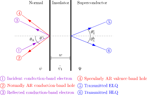
The relevant scattering processes at the N/S graphene interface are shown in Fig. 6, in the two cases of zero barrier and an insulating interface of width . In the former case, the boundary conditions dictate that , where
| (16) |
while in the latter case, one must match the wavefunctions at both interfaces:
| (17) |
where we have defined the wavefunction in the insulating region
| (18) |
The wavefunctions differ from in that the Fermi energy is greatly shifted by means of e.g. an external potential, such that where models the potential barrier (equivalent to the role of in Ref. btk, ). Also, note that the trajectories of the quasiparticles in the insulating region, defined by the angles and , differ by the same substitution, meaning
Finally, note that the subscript on the wavefunctions in the normal region indicates the direction of their group velocity, which in general is different from the direction of momentum, as discussed previously. Consequently, although the Andreev-reflected hole wavefunction carries a subscript ”” above, one should keep in mind that for normal Andreev reflection, the direction of momentum is opposite to the group velocity for the hole.
Before we go on to presenting results, we make one conceptual remark. The proximity effect means that an otherwise normal system becomes superconducting by virtue of having the superconducting wavefunction from a nearby superconductor leak into the normal system, thus making it superconducting in some region. This is a result of a boundary condition imposed on the normal system from the proximate host superconductor. The resulting wavefunction in the proximity region of the normal system is then a BCS type wavefunction. Such a wavefunction unquestionably describes a system with a gapped Fermi surface (possibly with nodes on the Fermi-surface). It matters not by what microscopic mechanism such a state was established, as long as it is there. The effective interaction giving rise to proximity induced superconductivity in graphene close to the surface in contact with an intrinsically superconducting host system, is obtained by considering the complete superconductor-graphene system and integrating out the electrons on the superconducting side. The electrons in graphene then experience an effective attractive interaction giving rise to a gap by virtue of hopping into and out of the superconducting side. We thus have, by such tunneling processes, even if . Here, is the electron-electron coupling constant giving rise to superconductivity in graphene per se. Since graphene intrinsically is a normal system, and is well approximated by non-interacting electrons, this coupling constant vanishes, . The relationship between the gap in the normal region and is thus , and this gives a nonzero gap in the vicinity of the proximate host superconductor. Here, are fermion annhilation operators, and thus represents the pair-amplitude induced in the normal graphene region. The proximity-induced gap vanishes rapidly as one goes away from the surface and into the bulk of graphene, since vanishes rapidly as we move away from the proximate host superconductor. It would in principle be incorrect to assert that in the proximity-region of graphene, we could have a non-zero anomalous Green’s function , but no gap , by using a self-consistency relation of the type with RevModPhys_2005 . Such a self-consistency relation does not exist in a normal system which does not superconduct by itself. However, in a situation where the intrinsic , it could well turn out to be the case that is small, leading to a gap which is very small bruder . In our paper, we have a thin film graphene system with a bulk superconductor in contact with the film, deposited on top of the film. If the thickness of the graphene-film is smaller than the coherence length of the bulk superconductor, one obtains a proximity-induced superconductiving gap throughout the film. As we shall see, our results are quite sensitive to the presence of even a small induced gap in graphene.
III Conductance spectra
In what follows, we describe how the conductance spectra of a N/S and N/I/S graphene junction may be obtained. According to the BTK formalism btk , the normalized conductance is given by
| (20) |
where and are the reflection coefficients for normal and Andreev reflection 222Note that in Ref. linderPRL07, , a factor was included as a prefactor of . While such a factor is present in the metallic case, it is absent for graphene junctions. Nevertheless, this does not affect the results of Ref. linderPRL07, in any manner since the case was considered there, implying ., respectively, while is a renormalization constant corresponding to the N/N metallic conductance kashiwaya96 ,
| (21) |
In this case, we have zero intrinsic barrier such that . We will apply the usual approximation , which may be shown to hold for a quite general parameter regime. For perfect normal reflection (), there is no conductance, while for perfect Andreev reflection (), the conductance is doubled compared to the N/N case. In order to obtain these coefficients, we make use of the boundary conditions described in the previous section. The analytical solution and behaviour of the conductance differs in the N/S and N/I/S case, and we proceed with a separate treatment of these scenarios.
III.1 N/S junction
Solving the boundary conditions for the wavefunctions at the interface leads to the analytical expressions for the reflection coefficients:
| (22) |
where we have defined the auxiliary quantities and The interplay between the different phases felt by the ELQ and HLQ in the superconductor in the case of an anisotropic order parameter enters above through the factor . It remains, however, to be clarified how this interplay manifests itself in the tunneling conductance. Before investigating this in more detail, let us briefly consider the isotropic -wave case first, i.e. , such that .
III.1.1 Conventional -wave pairing
For conventional superconducting pairing, Eq. (III.1) reduces to
| (23) |
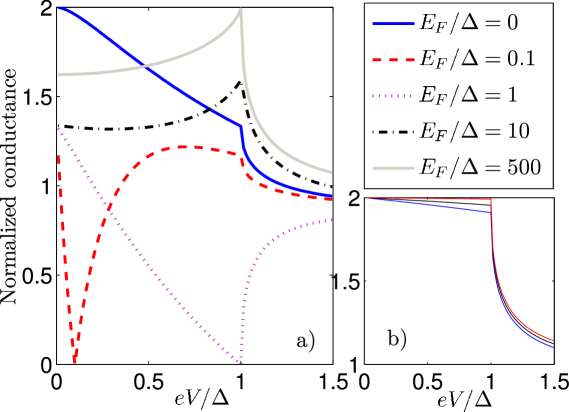
This case was first studied by Beenakker beenakker . For consistency and completeness, we reproduce the results of Ref. beenakker, [see Fig. 7a)]. We point out that Eq. (III.1.1) are valid for any parameter range, and not restricted to the heavily doped case treated in Ref. beenakker, . To illustrate the difference, we consider the regime shown in Fig. 7b). In this case, the standard situation of perfect Andreev reflection for subgap energies is recovered, with a sharp drop at the gap edge corresponding to the onset of quasiparticle transmittance into the superconductor.
III.1.2 Anisotropic -wave pairing
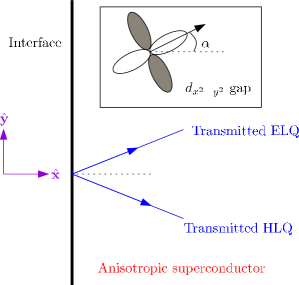
To treat an unconventional superconducting order parameter, we must revert to the general expressions in Eq. (III.1). In order to account for the effect of an anisotropic gap, we choose the -gap from Tab. 1, which in the weak-coupling approximation () reads . Here, models the relative orientation of the gap in -space with respect to the interface normal as illustrated in Fig. 8.
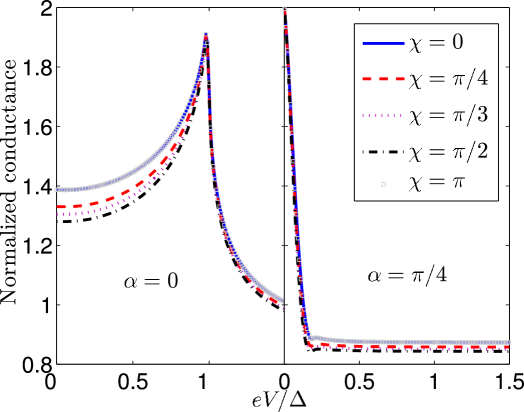
We now proceed to investigate how the conductance spectra of a N/S graphene junction change when going from a -wave to a -wave order parameter in the superconducting part of the system. Consider Fig. 9 for the case of heavily doped graphene, where the orientation of the gap is such that the condition for perfect formation of zero energy states in a metallic N/S junction is fulfilled, i.e. . As shown by Tanaka and Kashiwaya tanaka , this gives rise to a quasiparticle interference between the ELQ and HLQ since they feel different phases of the pairing potentials due to their different trajectories of transmittance into the superconductor. This results in a bound surface states with zero energy hu close to the N/S interface. For the N/S graphene junction studied here, the explicit barrier potential is zero, while FVM effectively acts as as source of normal reflection. From Fig. 9, one may infer that a peak at zero bias is present in the presence of FVM, although the ZBCP does not increase in magnitude with increasing FVM. We will later study how the presence of an intrinsic barrier in the form of a thin, insulating region separating the normal and superconducting part affects the ZBCP.
Next, we plot the conductance spectra for doped graphene to see how they evolve upon a rotation of the gap. The behaviour is quite distinct from that encountered in a N/S metallic junction. From Fig. 10a), we see that the peak of the conductance shifts from to progressively lower values as increases from to . In this respect, the conductance spectra actually mimicks a lower value of the gap than what is the case, if one were to infer the gap magnitude from the position of the singularity in the spectra. As of such, for a given FVM, determining the magnitude of the gap by the usual method of locating the characteristic feature in the conductance spectra is not as straight-forwards in N/S graphene junctions as in the metallic case. Indeed, multiple measurements with several different interface orientations would in general be required to obtain the correct value of the gap. This should be a unambigously observable feature in experiments, and provides a direct way of testing our theory. Finally, we consider graphene in Fig. 10b) with for a -wave order parameter. Upon varying from 0 to , there is now little distinction between different angles of orientation. The conductance spectra are in this case very resemblant to the metallic N/S case for zero barrier tanaka .
III.2 N/I/S junction
We now consider the conductance of an N/I/S graphene junction, where I denotes an ”insulating” (see introduction) region modelled by a very large energy potential for the quasiparticles. Solving the boundary conditions introduced in Sec. II, we obtain analytical expression for and , which is all that is required in order to calculate the conductance. However, these expressions are very large and the reader may consult Appendix A for their explicit form. In the following, we will not work exclusively in the thin barrier-limit as in Ref. sengupta, . Some aspects of including an insulation region of arbitrary width and strength were very recently discussed in Ref. sengupta2, , albeit only in the case of isotropic -wave pairing. We now treat the two cases of -wave and -wave pairing separately.
III.2.1 Conventional -wave pairing
This case was first studied by Bhattacharjee and Sengupta sengupta . To quantify the parameters in the insulating region, we will measure the width of region I in units of and the potential barrier in units of . First, we briefly show that we are able to reproduce the qualitative findings of Ref. sengupta, . As shown in Appendix A, it is convenient to introduce the parameter in the thin-barrier limit. In this case, the reflection coefficients and exhibit an interesting oscillating behaviour as a function of . To see this, consider Fig. 11 where we have plotted the voltage dependence of the normalized conductance for several values of . For , we reproduce the result of Fig. 7b). This is reasonable since the conductance of an N/I/S junction with , i.e. zero width, should be the same as an N/S junction. The -periodicity is reflected in that the curves for and are identical. For , , there is a source of normal reflection at the interfaces due to the insulating region, and consequently the subgap conductance is reduced from its ballistic value . Even in the presence of a FVM, , the spectra of Fig. 11 retain their -periodicity. However, the FVM acts as a source of normal reflection such that one does not have nearly perfect Andreev reflection at subgap energies.
Our results differ slightly from those reported in Ref. sengupta, . Although we obtain qualitatively exactly the same dependence on of the conductance, it is seen by comparing our Fig. 11 with Fig. 1 of Ref. sengupta, that our curves are phase shifted by in in comparison. As a consequence, we regain the N/S conductance result when instead of as reported in Ref. sengupta, . Physically, this seems to be more reasonable since corresponds to the case of an absent barrier, a situation where there is no source of normal reflection besides the condition that momentum in the direction parallell to the barrier must be conserved. We have also verified that our result coincides with the results obtained using the full expressions (see Appendix) without assuming a thin-barrier limit when we let both and go to zero. We believe that this minor discrepancy between our results and the results of Ref. sengupta, stems from a sign error in their Eq. (5) and also in their expression for in the text above Eq. (5).
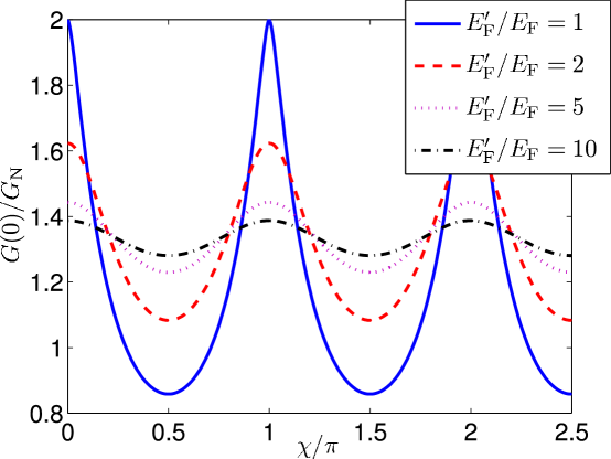
To unveil the periodicity even more clear, consider Fig. 12 for a plot of the zero-bias conductance as a function . The cases and display a striking difference. The qualitative shape of the curves is equal, but the amplitude is diminished with increasing FVM. This may in similarity to the above discussion be attributed to the increased normal reflection that takes place at zero bias voltage, thus reducing the conductance.
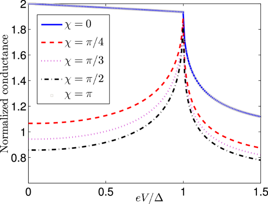
III.2.2 Anisotropic -wave pairing
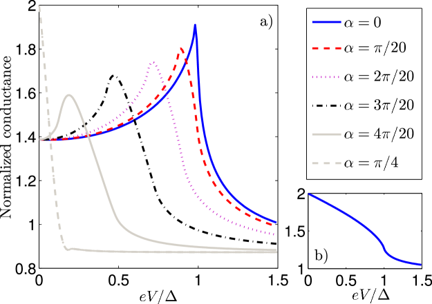
We now contrast the -wave case with an anisotropic pairing potential to see how the spectra are altered. Consider first Fig. 13 for a plot of the tunneling conductance in the undoped case. We consider the two angles and as representatives for the two types of qualitative behaviour that may be expected in a -wave superconductor/normal graphene junction. The latter corresponds to perfect formation of ZES in the metallic counterpart junction. From the spectra, one infers that for , tunneling into the nodes of the superconducting gap destroys the nearly perfect Andreev reflection for subgap energies obtained in Fig. 11. When , one observes the formation of a ZBCP which peaks at twice the normal state conductance. It is also interesting to note that the zero bias conductance remains unchanged upon increasing . Therefore, the equivalent of Fig. 12 in the present -wave case is , regardless of .
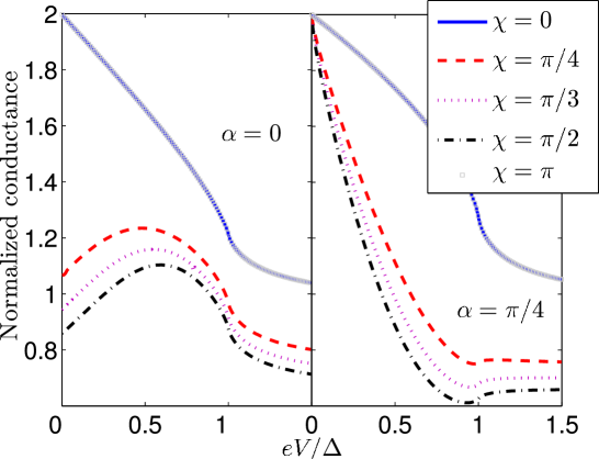
Introducing a FVM between the superconducting and normal parts of the system, the spectra are rendered less sensitive to any increase in , as seen in Fig. 14. For , the spectra are essentially identical to the doped -wave case. For , it is seen that the formation of a ZBCP becomes even more protruding, and that the zero bias conductance is still insensitive to any increase in . Therefore, one is led to conclude that the normalized zero bias conductance in the -wave case is constantly equal to nearly 2, regardless of and the magnitude of the FVM.
IV Conductance-oscillations
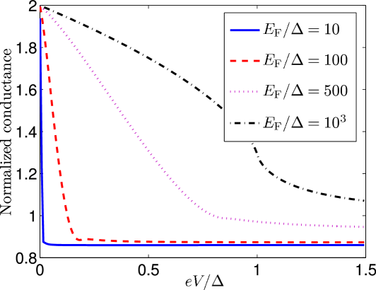
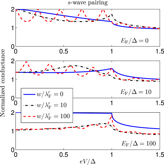
In this section, we investigate a feature of the conductance spectra that is in common for both the -wave and -wave case: an oscillatory behaviour as a function of applied bias voltage. Consider first a N/I/S graphene junction. In the thin-barrier limit defined as and with -wave pairing, Ref. sengupta, reported a -periodicity of the conductance with respect to the parameter , as discussed in the previous section. We now show that by not restricting ourselves to the thin-barrier limit, new physics emerges from the presence of a finite-width barrier. We measure the width of region I in units of and the potential barrier in units of . The linear dispersion approximation is valid wallace up to eV, and we will consider Fermi energies in graphene novoselov ranging from the undoped case meV to meV in the doped case, setting the gap value to meV. Owing to the restriction of , we fix , and also set in order to model the effective potential barrier.
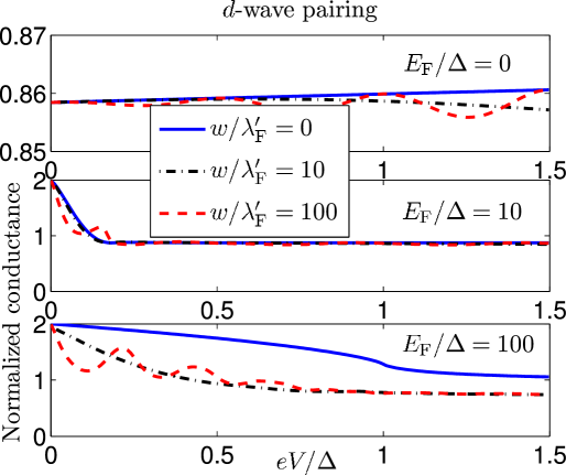
Consider Fig. 15 where we plot the normalized tunneling conductance in case of -wave pairing, for both a doped and undoped normal part of the system. The most striking new feature compared to the thin-barrier limit is the strong oscillations in the conductance as a function of . For subgap energies, we regain the N/S conductance for undoped graphene when , with nearly perfect Andreev reflection. The same oscillations are seen in the -wave pairing case, shown in Fig. 16. To model the -wave pairing, we have used the model with . The parameter effectively models different orientations of the gap in -space with regard to the interface, and corresponds to perfect formation of ZES in N/S metallic junctions. For , the -wave spectra are essentially identical to the -wave case, since the condition for formation of ZES is not fulfilled in this case tanaka . It is seen that in all cases shown in Figs. 15 and 16 the conductance exhibits a novel oscillatory behavior as a function of applied bias voltage as the width of the insulating region becomes much larger than the Fermi wavelength, i.e. .
The oscillatory behavior of the conductance may be understood as follows. Non-relativistic free electrons with energy impinging upon a potential barrier are described by an expontentially decreasing non-oscillatory wavefunction inside the barrier region if , since the dispersion essentially is . Relativistic free electrons, on the other hand, have a dispersion , such that the corresponding wavefunctions do not decay inside the barrier region. Instead, the transmittance of the junction will display an oscillatory behavior as a function of the energy of incidence . In general, a kinetic energy given by will lead to a complex momentum inside the tunneling region, and hence damped oscillatory behavior of the wave function. Relativistic massless fermions are unique in the sense that only in this case () is the momentum purely real. Hence, the undamped oscillatory behavior at sub-gap energies appears as a direct manifestation of the relativistic low-energy Dirac fermions in the problem. This observation is also linked to the so-called Klein paradox which occurs for electrons with such a relativistic dispersion relation, which has been theoretically studied in normal graphene katsnelson .
We next discuss why the illustrated conductance spectra are different for -wave and -wave symmetry, in addition to comparing the doped and undoped case. The difference in doping level between the superconducting and normal part of the system may be considered as an effective FVM, acting as a source of normal reflection in the scattering processes. This is why the subgap conductance at thin barrier limit is reduced when . Moving away from the thin barrier limit, it is seen that oscillations emerge in the conductance spectra. For -wave pairing, the amplitude of the oscillations is larger for than for the case of no FVM, but the period of oscillations remains the same. This period depends on , while the amplitude of the oscillations is governed by the wavevectors in the regions I and S. The maximum value of the oscillations occurs when equals an integer number of wavelengths, corresponding to a constructive interference between the scattered waves. Physically, the amplitude-dependence of the oscillations on the doping level originates with the fact that any FVM effectively acts as an increase in barrier strength. By making larger, one introduces a stronger source of normal reflection. When the resonance condition for the oscillations is not met, the barrier reflects the incoming particles more efficiently. This is also the reason why increasing directly and increasing the FVM has the same effect on the spectra.
We now turn to the difference between the -wave and -wave symmetries. It is seen that the conductance is reduced in the -wave case compared to the -wave case, and is actually nearly constant for . One may understand the reduction in subgap conductance in the undoped case as a consequence of tunneling into the nodes of the gap, which is not present in the -wave case. Hence, Andreev reflection which significantly contributes to the conductance, is reduced in the -wave case compared to the -wave case. Moreover, we see that a ZBCP is formed when , equivalent to a stronger barrier, and this is interpreted as the usual formation of ZES leading to a transmission at zero bias with a sharp drop for increasing voltage.
V Discussion
By means of the proximity effect, Heersche et al. successfully induced superconductivity in a graphene layer heersche (see also Ref. du, ). This achievement opens up a vista plethora of new, exciting physics due to the combination of the peculiar electronic features of graphene and the many interesting properties of superconductivity. For our theory to be properly tested experimentally, it is necessary to create N/S and N/I/S graphene junctions. Junctions involving normal graphene with insulating regions have recently been experimentally realized novoselov ; zhang . In our work, we have discussed novel conductance-oscillations in a N/I/S graphene junction that arise when moving away from the thin-barrier limit discussed in Ref. sengupta, . While reaching the thin-barrier limit might pose some difficulties from an experimental point of view, our predictions are manifested when using wide barriers, which should be technically easier to realize. In order to reach the doped regime, this could be achieved by either chemical doping or using a gate voltage to raise the Fermi level in the superconducting region katsnelson ; milton . The relevant magnitudes for the various physical quantities present in such an experimental setup has been discussed in the main text of this paper.
It is also worth mentioning that since we have assumed a homogeneous chemical potential in each of the normal, insulating, and superconducting regions, the experimental realization of the predicted effects require charge homogeneity of the graphene samples. This is a challenging criteria, since electron-hole puddles in graphene imaged by scanning single electron transistor martin suggest that such charge inhomogeneities probably play an important role in limiting the transport characteristics of graphene castro . In addition, we have neglected the spatial variation of the superconducting gap near the N/S interfaces. The suppression of the order parameter is expected to least pronounced when there is a large FVM between the two regions. However, the qualitative results presented in this work are most likely unaffected by taken into account the reduction of the gap near the interface.
VI Summary
In summary, we have studied coherent quantum transport in normal/superconductor (N/S) and normal/insulator/superconductor (N/I/S) graphene junctions, investigating also the role of -wave pairing symmetry on the tunneling conductance. We elaborate on the results obtained in Ref. linderPRL07, , namely a new oscillatory behaviour of the conductance as a function of bias voltage for insulating regions that satisfy , which is present both for - and -wave pairing. This is a unique manifestion of the Dirac-like fermions in the problem. In the -wave case, we have studied the conductance of an N/S and N/I/S junction in order to make predictions of what could be expected in experiments, providing both analytical and numerical results. We find very distinct behaviour from metallic N/S junctions in the presence of a FVM: a rotation of is accompanied by a progressive shift of the peak in the conductance, without any formation of a ZBCP except for . All of our predictions should be easily experimentally observable, which constitutes a direct way of testing our theory.
Acknowledgments
The authors are indebted to Takehito Yokoyama for very useful comments in addition to critical reading of the manuscript and the numerical code, and to Zlatko Tesanovic for helpful comunications. We have also benefited from discussions with Annica Black-Schaffer and Carlos Beenakker. This work was supported by the Norwegian Research Council Grants No. 158518/431 and No. 158547/431 (NANOMAT), and Grant No. 167498/V30 (STORFORSK). The authors also acknowledge the Center for Advanced Study at the Norwegian Academy of Science and Letters, for hospitality during the academic year 2006/2007.
Appendix A Normal- and Andreev-reflection coefficients for N/I/S junctions
Solving the boundary conditions Eq. (17), we obtain the following expressions for the normal reflection coefficient and the Andreev-reflection coefficient :
| (24) |
where the transmission coefficients read
| (25) |
with the definition
| (26) |
We have defined the auxiliary quantities
| (27) |
and similarly introduced
| (28) |
For more compact notation, we have finally defined
| (29) |
In the thin-barrier limit defined as and , one may set
| (30) |
where .
References
- (1) G. Deutscher, Rev. Mod. Phys. 77, 109 (2005).
- (2) C. W. J. Beenakker, Phys. Rev. Lett. 97, 067007 (2006).
- (3) C. Beenakker, arXiv:0710.3848v1 (2007).
- (4) K. S. Novoselov, A. K. Geim, S. V. Morozov, D. Jiang, Y. Zhang, S. V. Dubonos, I. V. Grigorieva, A.A. Firsov, Science 306, 666 (2004).
- (5) Y. Zhang, Y.-W. Tan, H. L. Stormer, P. Kim , Nature 438, 201 (2005).
- (6) In the quantum domain at low temperatures, and in the vicinity of the edge of the superconducting dome, the coupling between the nodal fermions in high- superconductors and quantum critical phase-fluctuations of the superconducting order parameter (i.e. vortices) will lead to unusual behavior. This has important ramifications for constructing a viable theory of the so-called pseudo-gap phase of these systems. See M. Franz and Z. Tesanovic, Phys. Rev. Lett. 87 257003 (2001); Z. Tesanovic, O. Vafek, and M. Franz, Phys. Rev B 65, 180511 (2002); O. Vafek and Z. Tesanovic, Phys. Rev. Lett. 91, 237001 (2003).
- (7) H. B. Heersche, P. Jarillo-Herrero, J. B. Oostinga, L. M. K. Vandersypen, A. F. Morpurgo, Nature 446, 56 (2007)
- (8) X. Du, I. Skachko, E. Y. Andrei, arXiv:0710.4984.
- (9) A. Yu. Kasumov, R. Deblock, M. Kociak, B. Reulet, H. Bouchiat, I. I. Khodos, Yu. B. Gorbatov, V. T. Volkov, C. Journet, M. Burghard, Science 284, 1508 (1999).
- (10) A. F. Morpurgo, J. Kong, C. M. Marcus, H. Dai, Science 286, 263 (1999).
- (11) M. R. Buitelaar, W. Belzig, T. Nussbaumer, B. Babic, C. Bruder, C. Schoenenberger, Phys. Rev. Lett. 91, 057005 (2003)
- (12) P. Jarillo-Herrero, J. A. van Dam, and L. P. Kouwenhoven, Nature (London) 439, 953 (2006).
- (13) S. Bhattacharjee and K. Sengupta, Phys. Rev. Lett. 97.
- (14) I. I. Mazin and M. D. Johannes, Nat. Phys. 1, 91 (2005).
- (15) J. Gonz lez, F. Guinea, M. A. H. Vozmediano, Phys. Rev. B 59, R2474 (1999).
- (16) C. L. Kane and E. J. Mele, Phys. Rev. Lett. 93, 197402 (2004).
- (17) K. S. Novoselov, A. K. Geim, S. V. Morozov, D. Jiang, M. I. Katsnelson, I. V. Grigorieva, S. V. Dubonos, and A. A. Firsov, Nature 438, 197 (2005).
- (18) J. Linder and A. Sudbø, Phys. Rev. Lett. 99, 147001 (2007).
- (19) C.-R. Hu, Phys. Rev. Lett. 72, 1526 (1994).
- (20) Y. Tanaka and S. Kashiwaya, Phys. Rev. Lett. 74, 3451 (1995).
- (21) P. R. Wallace, Phys. Rev. 71, 622 (1947).
- (22) G. E. Blonder and M. Tinkham, Phys. Rev. B 27, 112 (1983).
- (23) I. Zutic and O. T. Valls, Phys. Rev. B 61, 1555 (2000).
- (24) S. Kashiwaya, Y. Tanaka, M. Koyanagi, K. Kajimura, Phys. Rev. B 53, 2667 (1996).
- (25) C. Bruder, Phys. Rev. B 41, 4017 (1990).
- (26) A. Black-Schaffer and S. Doniach, Phys. Rev. B 75, 134512 (2007).
- (27) K. Fossheim, A. Sudbø, Superconductivity: Physics and applications, John Wiley & Sons Ltd., Ch. 5 (2004).
- (28) H. Kleinert, Phys. Rev. Lett. 84, 286 (2000).
- (29) Z. Tesanovic, Phys. Rev. B 51, 16204 (1995); ibid, B 59, 6449 (1999); A. K. Nguyen and A. Sudbø, Phys. Rev. B 57, 3123 (1998); ibid, B 58, 2802 (1998); ibid, B 60, 15307 (1999); Europhys. Lett. 46, 780 (1999).
- (30) F. S. Bergeret, A. F. Volkov, and K. B. Efetov, Rev. Mod. Phys. 77, 1321 (2005); A. I. Buzdin, Rev. Mod. Phys. 77, 935 (2005).
- (31) A. F. Volkov, P. H. C. Magnee, B. J. van Wees, and T. M. Klapwijk, Physica C 242, 261 (1995).
- (32) G. Fagas, G. Tkachov, A. Pfund, and K. Richter, Phys. Rev. B 71, 224510 (2005).
- (33) G. E. Blonder, M. Tinkham, and T. M. Klapwijk, Phys. Rev. B 25, 4515 (1982).
- (34) S. Bhattacharjee, M. Maiti, K. Sengupta, arXiv:0704.2760.
- (35) M. I. Katsnelson, K. S. Novoselov, A. K. Geim, Nature Phys. 2, 620 (2006)
- (36) J. Milton Pereira Jr., P. Vasilopoulos, and F. M. Peeters, cond-mat/0702596.
- (37) J. Martin, N. Akerman, G. Ulbricht, T. Lohmann, J. H. Smet, K. von Klitzing, and A. Yacoby, cond-mat/0705.2180 (2007).
- (38) E.-A. Kim and A. H. Castro Neto, arXiv:cond-mat/0702562 (2007).