Band Gap of CsCl Film’s as a Function of Lattice Constant.
Abstract
The manuscript reports experimental estimation of Cesium Chloride film’s band gap and compares it with theoretical simulations. The band gap shows a strong dependence on it’s lattice constant. Also, it is seen that the point defects present in the films strongly affects it’s optical properties.
I Introduction
In the past Alkali Halides (AH) were a topic of interest for crystallographers and researchers involved in energy band structure calculations. However, recently interest in AH have been renewed in connection with their optical properties for device applicationsr8 and optical wave guides.r9 Due to solubility of CsCl in its thin film state, Yoshikawa r77 did some limited amount of in situ characterization. Tsuchiya r17 have however taken advantage of CsCl’s high solubility and used its thin films as steam etch-able resists in IC fabrication. With such new applications of AH and in particular CsCl thin films and the lack of any extensive study of these materials in its thin film state, we were encouraged to study the optical properties of Cesium Chloride in thin film state for the present work. The present work consist details of structural, morphological and optical spectrum analysis done on Cesium Chloride films.
II Experimental
Thin films of Cesium Chloride were grown by thermal evaporation method using 99.98% pure starting material obtained from Loba Chemie Pvt Ltd, Mumbai. The films were grown on glass substrates kept at a distance of 12-15cm above the boat. The substrates were maintained at room temperature. Thin films were grown at vacuum better than -Torr. Films grown by this method were found to be slightly translucent with bluish to bluish-green tinge. The prelevance of color in these films were explained due to vacancies present in the films.rab ; ava Such vacancies would have resulted in the films as a result of possible dissociation of alkaline halide molecules when they are heated for evaporation.
III Results and Discussion
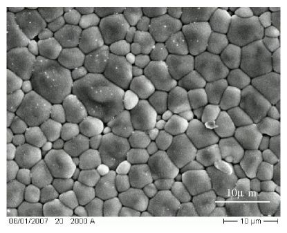
The structural studies of our films were done using Philips PW 3020 X-ray diffractometer. The as grown films of CsCl were found to be polycrystalline in nature. The peak positions match those listed in ASTM Card No.05-0607. The polycrystalline nature of the films were also confirmed by studying the surface morphology of the films (fig 1) using JEOL (JSM)-840 Scanning Electron Microscope (SEM). Optical characterization of our samples were carried out using the UV-visible spectroscope (Shimadzu’s UV 2501-PC). Since CsCl has a very large band-gap, the absorption edge lies in the UV region. The absorption data in visible range, hence can not be used to determine the energy band gap using the conventional Tauc’s methodr218 . However, indirect estimation of the band-gap can still be made from the absorption spectra in a region away from the band edge. In fact, it has been shown that the optical absorption coefficient of semiconductors and insulators vary exponentially with incident photon energy away from the band edge.Urb The behavior is called the Urbach tail and the absorption coefficient is related to the photon energy askurik
| (1) |

where is the extrapolated band-gap and , the absorption coefficient of the material at the band-gap energy. is called the Urbach energy. The values of Urbach energy can be determined from the slope of the best fit straight line
| (2) |
We have fit eqn(2) on our absorption data and have estimated the values of . Using this result, the band gap of the films were extrapolated from the intercepts obtained by fitting eqn(2) to our data. A plot of such an estimated with increasing lattice constants shows a decreasing trend (fig 2). The displacement of Cs and Cl atoms, moving away from each other with increasing lattice constant maybe the cause of decreasing band gap. Increasing atomic distances would decrease the effective lattice potentials as seen by the electrons producing appreciable change in band gap.


To substantiate this we have theoretically calculated the band structure to investigate the variation in energy band gap with varying lattice constant. For our calculations we have used the Full-Potential Linearized Augmented Plane Wave (FP-LAPW) method within the density functional theory (DFT) as implemented by the WIEN2k code. WIEN2k In fig 3, we compare the band structures of bulk CsCl with lattice parameters (a) of CsCl in single crystal state (=0.412nm) and (b) at 0.4236nm. The figure shows the region R X that forms the minimum gap. In both cases we have a direct transition band gap, located at the point. The main difference corresponds to the bottom of the conduction band at the point, since at the equilibrium lattice constant three bands forming the bottom of the conduction band are degenerated at the point, while at the higher lattice constant the degeneration is broken and a band splits down in energy, with the main difference of 0.37 eV at the point. The breaking of degeneracy is observed in all simulations where the lattice constant is considered more than 0.412nm. The variation in band gap with increasing lattice constant was theoretically simulated (see fig 4). The valence bands maintains its structure in all cases, although negligible differences can be observed for the top of the valence band in the direction.

The theoretical calculations also show a similar decreasing trend in band-gap with increasing lattice constant as our experimental results. However, fig 4 does not indicate a large variation in band-gap with lattice constant as indicated in fig 2. As stated earlier, our films were colored indicating the existence of vacancies in our films. Hence we repeated our calculations for band gap, however, in this case with one chlorine atom absent per 27 unit cells. Fig 4 compares the two results. A chlorine atom vacancy in 27 unit cell leads to a reduction of 0.3eV in the material’s band gap. This variation is nearly constant throughout the range of increase in lattice constant studied. The scattering of our data points and large variation in our band gap (fig 2) might be explained by combined effect of increasing lattice constant and unsystematically variation in number of vacancies. We believe these characterizations can be of use for controlled fabrication of optical devices or optical waveguides using CsCl.
IV Conclusions
The optical properties of thin films of CsCl are found to strongly depend on the unit cell’s lattice constant and the vacancies present in it. The vacancies give rise to energy levels within the forbidden gap which results in giving a color to the hitherto transparent film. Similarly, increasing lattice size results in larger inter-atomic distances between neighboring atoms that results in breaking of degeneracy of energy levels that in turn affects the material’s band gap.
Acknowledgment
The help in completing the spectroscopic and diffraction analysis by Mr. Dinesh Rishi (USIC), Mr. Padmakshan and Mr. Rohtash (Department of Geology, Delhi University) is also acknowledged. L.M. and E.A.A. acknowledge financial support from the Consejo Nacional de Investigaciones Científicas y Técnicas (CONICET), the Universidad Nacional de Entre Ríos (UNER), and the Agencia Nacional de Promoción Científica y Tecnológica (ANPCyT), Argentina.
References
- (1) S. Asaka, M. Itoh, M. Kamada, Phys. Rev. B, 63 (2001) 081104.
- (2) M. Cremona, J. A.M. Perira, S. Pelli, G.C. Righini, Applied Phys. Lett., 81 (2002) 4103.
- (3) G. Yoshikawa, M. Kiguchi, K. Ueno, A Koma, K.Saiki, Surfaces Science, 544 (2003) 220-226.
- (4) Shin Tsuchiya, Mino Green and R.R.A. Syms, Electrochemical and Soild State Letters, 3 (2000) 44-46.
- (5) H. Rabin and J. H. Schulman, Phys. Rev. 125 (1962) 1584.
- (6) P. Avakian and A. Smakula, Phys. Rev. 120 (1960) 2007.
- (7) J. Tauc, ”Amorphous and Liquid Semiconductors”, J. Tauc Ed. (Plenum, London, 1974).
- (8) F. Urbach, Phys Rev, 92, 1324 (1953).
- (9) M. V. Kurik, Phys. Status Solidi A, 8 9 (1971).
- (10) P. Blaha, K. Schwarz, J. Luitz, Viena University of Technology (2001). (Improved and updated version of the WIEN code, published by P. Blaha, K. Schwarz, P. Sorantin and S. B. Rickey, Comp. Phys. Commun. 59 (1990) 399.