Modeling a Schottky-barrier carbon nanotube field-effect transistor with ferromagnetic contacts
Abstract
In this study, a model of a Schottky-barrier carbon nanotube field-effect transistor (CNT-FET), with ferromagnetic contacts, has been developed. The emphasis is put on analysis of current-voltage characteristics as well as shot (and thermal) noise. The method is based on the tight-binding model and the non-equilibrium Green’s function technique. The calculations show that, at room temperature, the shot noise of the CNT FET is Poissonian in the sub-threshold region, whereas in elevated gate and drain/source voltage regions the Fano factor gets strongly reduced. Moreover, transport properties strongly depend on relative magnetization orientations in the source and drain contacts. In particular, one observes quite a large tunnel magnetoresistance, whose absolute value may exceed 50%.
pacs:
85.75.Hh, 75.47.De, 42.50.Lc, 73.63.Fg1 Introduction
In view of well-known size reduction problems of the conventional Si-based electronics, there have recently been intensive studies on new technologies based on nanostructured materials which are formed by organized growth and self-assembly methods [1]. A remarkable example of such self-organized structures are carbon nanotubes, which due to their fascinating physical properties have been studied for more than one and a half decade now and are believed to have commercial applications in the near future. In particular a nanotube-based transistor was first demonstrated in [2], and has since been studied extensively ([3]-[5]). Carbon nanotubes are also very promising for spintronic applications, they may act as magneto-resistive switches [6, 7], and can maintain spin coherence over long distances. The latter is crucial for the tunnel (giant) magnetoresistance TMR (GMR) effect to be observable. In fact the TMR effect in CNTs was first reported in [8], where the spin diffusion length of electrons flowing through a carbon tube was estimated to be on the order of routinely used contact separations in electric transport measurements. Subsequent studies confirm that the TMR effect in CNTs can be quite large, ranging typically from a few up to several tens percent ([9]-[15]). Here it is shown that also for the Schottky-barrier nanotube transistor the situation is likewise.
Shot noise is another important phenomenon of present interest. It only appears in a non-equilibrium situation (finite source/drain voltage) and originates from the discreteness of the electron charge. In spite of there being a lot of papers on shot noise in nanostructures ([16]-[19]) (see [20] for a comprehensive review of recent advances), there have hitherto been no attempts to investigate shot noise in ferromagnetically contacted Schottky-barrier nanotube transistors (to the author’s knowledge).
The paper is organized in the following way: In Sec. 2 a short discussion of the adopted approach is presented, including the way the electrostatics has been dealt with, and basic equations concerning the non-equilibrium Grean’s function method. Section 3 is devoted to main results of the paper, i.e. current and shot noise dependences on the gate and drain/source voltages, as well as the impact of ferromagnetic electrodes on the above mentioned transport characteristics. Finally, Sec. 4 concludes the papers.
2 Methodology
A nanotransistor under consideration consists of a single wall carbon nanotube (CNT), described in terms of -orbital electrons, end-contacted to s-type itinerant-electron slabs of fcc (111) crystallographical structure. The latter may be either paramagnetic or ferromagnetic. The system considered here is end-contacted, in contrast to other wide-spread geometries, like those of side-contacted or embedded ones. The device has been relaxed in order to find energetically favorable positions of interface atoms represented by big and small spheres with diameters of and , for metal and carbon, respectively [10, 11]. The studies are carried out within the framework of the tight-binding model and the non-equilibrium Green’s function technique. The basic idea of this study is to adopt the methodology known for one-dimensional transistor models [21, 22, 23], so as to make it useful for description of a Schottky-barrier nanotube transistor. This method bears much similarity to earlier methods [24, 25, 26], except that here the calculations are performed in real space for CNT of finite length, and there is no need of using any ideal nanotube energy spectra (nor the Wentzel-Kramers-Brilloin, WBK, approximation). It should be however stated in this context that there is a great deal of theoretical studies on nanotube transistors (see e.g [27]-[31]), which successfully avoid reducing the Poisson equation to the 1-D problem, and handle thereby the electrostatics on a higher level than it is done here. Nevertheless, the present approach, while benefiting enormously from the mathematical simplicity, still leads to qualitatively correct results. The one-dimensional Poisson equation and its solutions are regarded here as spin-dependent(however spin indexes are skipped for brevity), and read [21]
| (1) |
| (2) |
| (3) |
| (4) | |||||
where is the effective screening length [23], and stand for the dielectric constant and the radius of the CNT, whereas the subscript refers to the coaxial gate oxide layer ( in thickness). The other symbols have the following meaning: , , - source, drain and gate voltages; - the length of the CNT; - Fermi function at and ; - the CNT cross-sectional area.
As regards the non-equilibrium Green’s function (GF) technique, a recursive method, similar to that of [32] was used, with obvious modifications consisting in including the potential profile V(x) (Eq. 2) to the CNT Hamiltonian, and the and voltages in the contacts. This procedure corresponds to the Hartree approximation, which is sufficient for the present room-temperature model, far beyond the Coulomb blockade and Kondo regimes. With this proviso one can write down equations for spin-projected current (I), zero-frequency noise power (S) and transmission matrix (T) as follows
| (5) |
where trace () is taken over the orbital indexes, and (with S, D for source and drain, respectively). The first term of the noise power S is the thermal noise, it disappears at zero temperature, but dominates at finite temperatures and vanishing source/drain potentials. The Fano factor is defined here - assuming that both spin channels are independent (no spin relaxation processes) - in a usual way as , so that it is one for the Schottky shot noise (Poissonian limit).
Instead of a rather common wide-band type approximation, the present method uses energy-dependent self-energies () which have been expressed in terms of: (i) recursively computed surface Green functions () of infinite fcc-(111) contacts, and (ii) the CNT/contact coupling matrices (), i.e . Here the retarded, , (advanced, ) GF is a matrix of rank equal to the number of atoms in the unit cell it refers to. The density matrix is defined as in terms of the lesser GF, which can be brought into the following form: While integrating , its first term contribution is found by integral over the contour in the complex energy plane, and the second one - by integrating along the real energy axis (using the Gaussian quadrature). The so-determined integral makes it possible to get an extra (excess or deficit) electric charge per CNT atom, with respect to the charge neutrality situation (no external potentials). The procedure is self-consistent because the potential enters the diagonal of the Hamiltonian, which in turn, is present in the GF denominator. In order to make the recursive algorithm effectively work, and speed up the convergence, an additional assumption has been made, viz. the potential profile is only dependent on the unit cell number and remains constant within the given unit cell.
3 Results and discussion
Detailed computations have been carried out for a zigzag semiconducting CNT with a chiral vector (n, 0) and n=14. The radius , and the energy gap , where a=0.249 nm is the graphene lattice constant and eV is the -orbital hopping integral. Additionally, it has been set: , , nm. The CNT is unit cells long (), and the calculations are performed for (as well as for the ultra-short length ). It is well known that the Schottky-barrier at a semiconductor/metal interface depends mainly on relative work functions (WF) of materials which form the junction [30, 31, 33]. Here it is assumed that the metal WF is greater than that of the CNT, as e.g. for Pt, Au, Ni, Fe (as opposite to Ti), and locate the Fermi energies below the mid-gap. To be specific, the metal Fermi energy has been fixed at one-quarter of the band gap. On- and off-states of the FET are illustrated in Inset to Fig. 1, where the lower curves correspond to the maximum of the valence band and the upper curves correspond to the minimum of the conduction band.
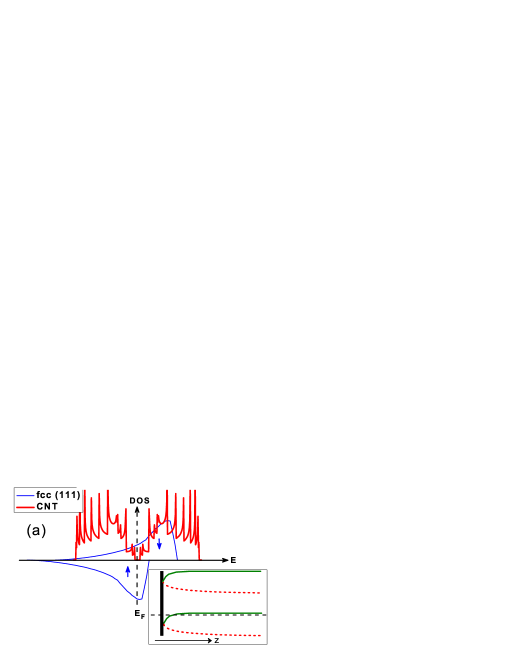
Accordingly, the present model-device represents an ” close to valence band maximum” case (cf. [4]). It is seen that, depending on the gate-voltage, the CNT-FET is either in the on-state (solid lines) or the off-state (short-dash lines). The former is due to the hole tunnelling through the Schottky-barrier, whereas the latter results from the fact that the transport energy-window falls within the energy gap. The location of beyond the mid-gap of the isolated CNT introduces the electron-hole asymmetry, as shown recently [34] a similar effect may be caused by the presence of the inner uncontacted shell in a double-walled CNT, leading essentially to similar results for current-voltage characteristics (in the non-magnetic case).
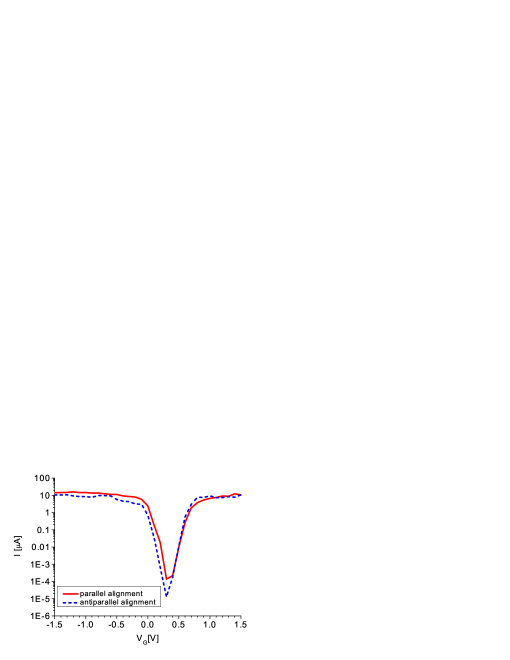
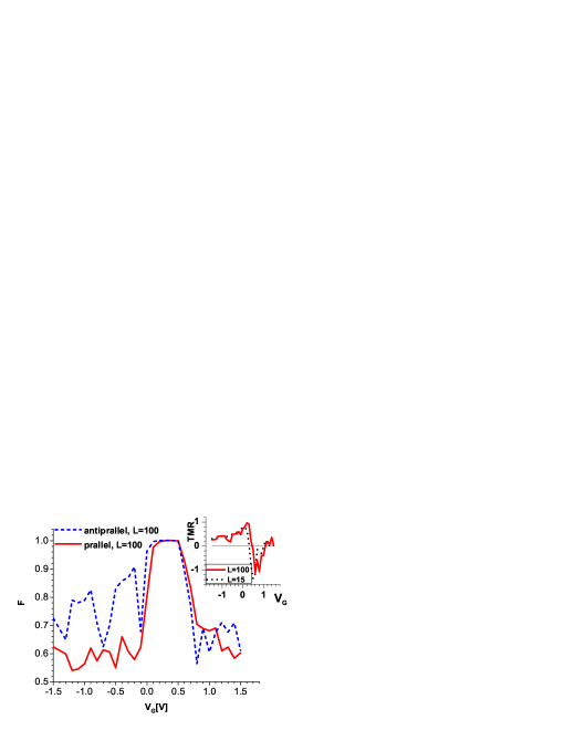
Figure 2 clearly shows that depending on boundary conditions imposed by the magnetic contacts [parallel alignment (P) vs. antiparallel alignment (AP)] the current-gate voltage characteristics differ considerably from each other. Notably, the ON/OFF current ratio is also different for both the alignments. This is because the sub-threshold region reveals a conventional (Julliere’s type [35]) behavior with clearly greater than , whereas beyond this region both the currents differ far less from each other. Within the ”non-Julliere’s” region the negative TMR apparently appears as a result of the shift of threshold for electron conduction between P and AP configurations. Figure 3 presents the corresponding Fano factors. The shot noise of the CNT FET is Poissonian (F=1) in the sub-threshold region, and gets substantially reduced for elevated and . A still stronger reduction would be possible if the transport regime e.g. was either ballistic or of electron billiard type (with a short dwell time) [16, 36]. As expected, magnetic conditions of the contacts, which strongly influence the current, have also a considerable effect on the noise. It is readily seen from Fig. 3 that the Fano factor corresponding to the P alignment, when compared to that of the AP alignment, is predominantly suppressed. The suppression takes place in a large region of the gate voltage, where current in the P configuration is greater than in the AP configuration (cf. Fig. 2), in concord with the fact that . It should be stressed that the transport regime considered here is phase coherent, although with noticeably reduced transmission due to the presence of Schottky-barriers. That is why the length effects, as shown in the Inset to Fig.3, are quite moderate, in contrast to what could be expected in the diffusive transport regime. Spin-dependent electron wave interferences are responsible for non-monotonic behavior of presented plots and accompanying sharp features. Similar features have been reported both in conductance and TMR [9, 13, 37] as well as in the differential Fano factor [19].
The TMR is defined here in a ”pessimistic” way as , where () is the current
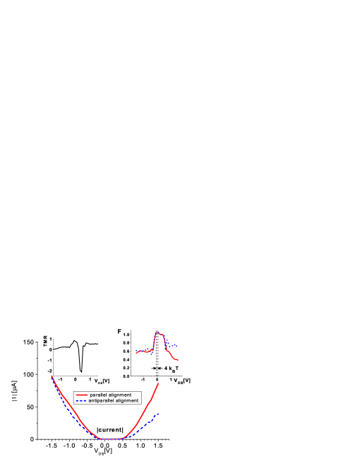
flowing through the system in the P (AP) magnetic configuration. The calculations are performed for spin polarizations in the ferromagnetic contacts equal to ( is the number of -spin electrons per atom). The results concerning TMR against and are presented in Figs. 3 and 4, respectively. The corresponding Insets clearly show that the TMR absolute value may be quite substantial and exceed several tens percent both in the sub-threshold region and at elevated voltages. Interestingly enough, TMR can assume large negative values (inverse TMR) and is strongly sensitive to both the gate- and -voltages. Another important observation is a striking asymmetry of the Fano factor and the GMR effect with respect to the sign of the voltage (-channel vs. -channel). These features are due to the aforementioned location of with respect to the mid-gap, which makes the Schottky barrier for electrons higher than that for holes, and consequently the hole current (for negative voltages) is higher than the electron current (for positive voltages). It is noteworthy, that the oscillations present in Figs. 2-4 are due to the size-dependent quantization of the CNT energy-levels, so the local maxima (minima) therein depend on to which extent the voltage-driven active channels and the transport energy-window fit together. This mechanism is also responsible for the occurrence of the inverse GMR, in fact it is similar to the mechanism based on resonant tunneling suggested in [12].
4 Conclusions
An approach has been developed to describe nanotube transistors, which combines a simplified (analytical) treatment of the electrostatics, and the state-of-the-art non-equilibrium GF technique. Unprecedented studies of electric transport through Schottky-barrier CNT transistor with ferromagnetic electrodes have been carried out. It has been shown that the tunnel ability of particles depends strongly on the alignment of contact magnetizations. Remarkably, the tunnel magnetoresistance can exceed 50%, whereas the Fano factor is usually subjected to some extra suppression when the magnetization alignment gets reoriented from the antiparallel to the parallel one, improving thereby the noise-to-signal ratio. These two findings are relevant for prospective applications of nanotubes in spintronics.
References
References
- [1] Hoenlein W et al 2006 Microelectron. Eng. 83 619
- [2] Tans S, Verschueren A, and Dekker C 1998 Nature 393 49
- [3] Léonard F and Tersoff J 1999 Phys. Rev. Lett. 83 5174
- [4] Heinze S, Tersoff J, Martel R, Derycke V, Appenzeller J and Avouris P, Phys. Rev. Lett. 2002 89 106801
- [5] Javey A, Guo J, Wang Q, Lundstrom M, and Dai H 2003 Nature 424 654
- [6] Coskun U C, Wei T-C, Vishveshwara S, Goldbart P M, and Bezryadin A 2004 Science 304 1132
- [7] Zaric S et al 2004 Science 304 1129
- [8] Tsukagoshi K, Alphenaar B W and Ago H 1999 Nature 401 572
- [9] Mehrez H, Taylor J, Guo H, Wang J and Roland C 2000 Phys. Rev. Lett. 84 2682
- [10] Krompiewski S 2006 Semicond. Sci. Technol. 21 S96
- [11] Krompiewski S 2005 physica status solidi (b) 242 226
- [12] Cottet A et al 2006 Semicond. Sci. Technol. 21 S78
- [13] Cottet A and Choi M-S 2006 Phys. Rev. B 74 235316
- [14] Jensen A, Hauptmann J R, Nygard J and Lindelof P E 2005 Phys. Rev. B 72 035419
- [15] Hueso E et al 2007 Nature 445 410
- [16] Blanter Ya M and Büttiker M 2000 Phys. Rep. 336 1
- [17] Onac E et al 2006 Phys. Rev. Lett. 96 026803
- [18] Tersoff J 2007 Nano Lett. 7 194
- [19] Wu F, Queipo P, Tsuneta T, Wang T H, Kauppinen E and Hakonen P J, cond-mat/0702332
- [20] Blanter Ya M, arXiv:cond-mat/0511478
- [21] Indlekofer K M, Knoch J and Appenzeller J 2005 Phys. Rev. B 72 125308
- [22] Pikus F G and Likharev K K 1997 Appl. Phys. Lett. 71 3661
- [23] Auth P and Plummer J D 1997 IEEE El. Dev. Lett. 18 74
- [24] Odintsov A A 2000 Phys. Rev. Lett. 85 150
- [25] Nakanishi T, Bachtold A, and Dekker C 2002 Phys. Rev. B 66 073307
- [26] Anantram M P and Léonard P 2006 Rep. Prog. Phys. 69 507
- [27] Guo J, Datta S, Lundstrom M 2004 IEEE Transactions on Electron Devices 51 (2) 172
- [28] John D, Castro L, Pereira P and Pulfrey D, in: Proceedings of the NSTI Nanotech 3, Boston, USA, 2004, pp. 65 68
- [29] Anantram M P, Lundstrom M S and Nikonov D E, cond-mat/0610247
- [30] Chen Z, Appenzeller J, Knoch J, Lin Y and Avouris P 2005 Nano Lett. 5 1497
- [31] L eonard F and Stewart D A 2006 Nanotechnology 17 4699
- [32] Krompiewski S, Martinek J and Barnaś J 2002 Phys. Rev. B 66 073412
- [33] Nosho Y, Ohno Y, Kishimoto S, and Mizutani T 2006 Nanotechnology 17 3412
- [34] Wang S and Grifoni M 2007 Phys. Rev. B 76 033413
- [35] Julliere M 1975 Phys. Lett. A 54 225
- [36] Beenakker C and Schönenberger C 2003 Physics Today (May) 37
- [37] Man H T, Wever I J W and Morpurgo A F 2006 Phys. Rev. B 73 241401