Design and Implementation of the New D0 Level-1 Calorimeter Trigger
Abstract
Increasing luminosity at the Fermilab Tevatron collider has led the D0 collaboration to make improvements to its detector beyond those already in place for Run IIa, which began in March 2001. One of the cornerstones of this Run IIb upgrade is a completely redesigned level-1 calorimeter trigger system. The new system employs novel architecture and algorithms to retain high efficiency for interesting events while substantially increasing rejection of background. We describe the design and implementation of the new level-1 calorimeter trigger hardware and discuss its performance during Run IIb data taking. In addition to strengthening the physics capabilities of D0, this trigger system will provide valuable insight into the operation of analogous devices to be used at LHC experiments.
keywords:
Fermilab, DZero, D0, trigger, calorimeterPACS:
29.40.Vj, 07.05.Hd1 Introduction
During the five year period between the end of Run I in 1996 and the beginning of Run IIa in 2001, the Fermilab Tevatron accelerator implemented an ambitious upgrade program [1] in which the proton–antiproton center of mass energy was increased from 1.8 TeV to 1.96 TeV and the instantaneous luminosity was boosted by an order of magnitude. To take advantage of the new accelerator conditions, the collider experiments, CDF and D0, also embarked on major upgrades to their detectors.
The D0 upgrade, described fully in [2], involved a complete replacement of the Run I tracking system with a new set of silicon micro-strip and scintillating fiber trackers as well as the addition of a 2 T solenoid magnet. Although the uranium and liquid argon calorimeter was left unchanged, its electronics were overhauled to match the new Tevatron bunch structure, and a series of preshower detectors was added outside of the solenoid to help measure energy of electrons, photons, and jets. Muon detection was improved with the addition of new detectors and shielding. Finally, the trigger and data acquisition systems were almost completely redesigned.
As originally proposed [1], approximately 20 times the integrated luminosity delivered in Run I was scheduled to be accumulated during Run II, for a total of 2 fb-1. To accomplish this goal major improvements were made to all aspects of the Tevatron, particularly in the areas of antiproton production. The bunch structure of the machine was also changed to accommodate 3636 bunches of protonsantiprotons, with an inter-bunch spacing of 396 ns, which is an improvement over the 66 mode of operation in Run I. Future enhancements to 132 ns inter-bunch spacing were also foreseen, motivating a Tevatron RF structure with 159 potential bunch crossings (separated by 132 ns) during the time it takes a proton or antiproton to make a single revolution, or turn around the Tevatron. Of these potential crossings, only 36 contain actual proton–antiproton collisions.
Driven by ambitious physics goals of the experiments, a series of continued Tevatron improvements was also planned [3], beyond the Run II baseline, with the aim of increasing the total integrated luminosity collected to the 4 – 8 fb-1 level. To achieve this performance, instantaneous luminosities in excess of 21032 cm-2s-1 are required. Tevatron upgrades for this period include fully commissioning the Recycler as a second stage of antiproton storage and implementing electron cooling in the Recycler. The majority of these improvements were successfully completed during a Tevatron shutdown lasting from February to May 2006, which marks the beginning of Run IIb.
The long-term effects of the Run IIb Tevatron upgrade on the D0 experiment are threefold. First, the additional integrated luminosity to be delivered to D0 during the course of Run IIb will also increase the total radiation dose accumulated by the silicon detector. Best estimates indicate that such a dose will compromise the performance of the inner layer of the detector, affecting the ability of D0 to tag -quarks – a necessary ingredient in much of the experiment’s physics program. Second, the increased instantaneous luminosity stresses the trigger system, decreasing the ability to reject background while maintaining high efficiency for signal events. And finally, the plan of having real bunch crossings separated by 132 ns, although not realized in the final Run IIb configuration, would have created problems matching calorimeter signals with their correct bunch crossing in the Run IIa calorimeter trigger system.
The first of the effects mentioned above led D0 to propose the addition of a radiation-hard inner silicon layer (Layer-0) to the tracking system [4]. The second and third effects required changes to various aspects of the trigger system [5]. These additions and modifications, collectively referred to as the D0 Run IIb Upgrade, were designed and implemented between 2002 and 2006 and were installed in the experiment during the 2006 Tevatron shutdown.
In the following we describe the Level-1 Calorimeter Trigger System (L1Cal) designed for operation during Run IIb. Section 2 contains a brief description of the Run IIa D0 calorimeter and the three-level trigger system. Section 3 discusses the motivation for replacing the L1Cal trigger, which was used in Run I and Run IIa. Algorithms used in the new system and their simulation are described in Sections 4 and 5, while the hardware designed to implement these algorithms is detailed in Sections 6, 7, 8, and 9. Mechanisms for online control and monitoring of the new L1Cal are outlined in Sections 10 and 11. This article then concludes with a discussion of early calibration and performance results in Sections 12 and 13, with a summary presented in Section 14.
2 Existing Framework
2.1 The D0 Calorimeter
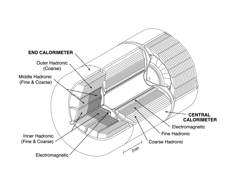
The basis of the Run IIb L1Cal trigger is the D0 calorimeter, described in more detail in [2, 6]. This detector, shown schematically in Fig. 1, consists of three sampling calorimeters (a barrel and two endcaps), in three separate cryostats, using liquid argon as the active medium and depleted uranium, uranium-niobium alloy, copper or stainless steel as the absorber. It also includes detectors in the intercryostat region (ICR), where the barrel and endcaps meet, consisting of scintillating tiles, as well as instrumented regions of the liquid argon without absorbers. The calorimeter has three longitudinal sections – electromagnetic (EM), fine hadronic (FH) and coarse hadronic (CH) – each themselves divided into several layers. It is segmented laterally into cells of size 0.10.1 [7] arranged in pseudo-projective towers (except for one layer in the EM section, which has 0.050.05). The calorimeter system provides coverage out to 4.
Charge collected in the calorimeter is transmitted via impedance-matched coaxial cables of 10 m length to charge sensitive preamplifiers located on the detector. The charge integrated output of these preamplifiers has a rise time of 450 ns, corresponding to the electron drift time across a liquid-argon gap, and a fall time of 15 s. The single-ended preamplifier signals are sent over 25 m of twisted pair cable to Baseline Subtractor (BLS) cards.

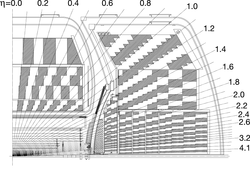
On the 1152 BLS cards, the preamplifier signals are split into two paths: the precision readout and the trigger sum pickoff. Precision readout path signals for each calorimeter cell are shaped, baseline subtracted, and stored in a set of switched capacitor arrays awaiting Level-1 and Level-2 trigger decisions. Signals on the trigger sum pickoff path, shown in Fig. 2 are shaped to a triangular pulse with a fast rise and a linear fall over 400 ns. They are then passed to analog summers that add signals in different cells, weighted appropriately for the sampling fraction and capacitance of each cell to form EM and HD trigger towers (TT). EM TTs contain all cells (typically 28) in 0.20.2 regions of the EM section of the calorimeter, while HD TTs use (typically 12) cells in the FH section of the calorimeter to form 0.20.2 regions. This granularity leads to 1280 EM and 1280 HD TTs forming a 4032 grid in space, which covers the entire azimuthal region for 4.0. Due mainly to overlapping collisions, which complicate the forward environment, however, only the region 3.2 is used for triggering.
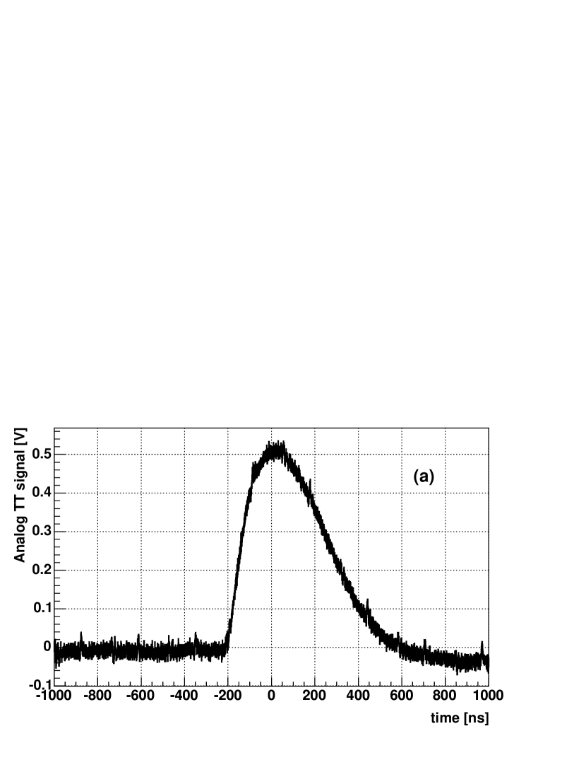
The EM and HD TT signals are transmitted differentially to the Level-1 Calorimeter Trigger electronics on two separate miniature coaxial cables. Although the signal characteristics of these cables are quite good, some degradation occurs in the transmission, yielding L1Cal input signals with a rise time of 250 ns and a total duration of up to 700 ns. Typical EM and HD TT signals are shown in Fig. 3.
2.2 Overview of the D0 Trigger System
The D0 experiment uses a three level trigger system, shown schematically in Fig. 4 and described in more detail in [2], to select interesting events from the 1.7 MHz of bunch crossings seen in the detector. Individual elements contributing to the Level-1 (L1) and Level-2 (L2) systems, as used in Run IIb, are shown in Fig. 5.

The L1 trigger system, implemented in custom hardware, examines data from the detector for every bunch crossing. It consists of separate elements for calorimeter (L1Cal), scintillating fiber tracking (L1CTT), muon (L1Muon), and forward proton (L1FPD) data. New for Run IIb is an element that matches tracks and calorimeter clusters at L1 (L1CalTrk), which is functionally similar to L1Muon. Each L1 trigger element sends its decisions on a set of criteria (for example, the presence of two jets with transverse energy above a threshold) to the trigger framework (TFW). The TFW uses these decisions, referred to as the and/or terms to decide whether the event should be accepted for further processing or rejected. Because of the depth of data pipelines in the detector’s front end electronics, L1 decisions from each of the trigger elements must arrive at the TFW within 3.7 s of the bunch crossing producing their data. This pipeline depth was increased from its Run IIa value of 3.3 s in order to accomodate the extra latency induced by the L1CalTrk system. After an L1 accept, data are transferred off of the pipelines, inducing deadtime in the system. The maximum allowable L1 accept rate, generally around 2 kHz, is set by the desire to limit this deadtime to the 5% level.
The L2 system receives data from the detector and from the L1 trigger elements on each L1 accept. It consists of detector-specific pre-processor engines for calorimeter (L2Cal); preshower (L2PS); scintillating fiber (L2CTT) and silicon (L2STT) tracking; and muon (L2Muon) data. Processed data from each of these elements is transmitted to a global processor (L2Global) that selects events based on detector-wide correlations between its input elements. The L2 trigger operates at a maximum input rate of 2 kHz and provides L2 accepts at a rate of up to 1 kHz.
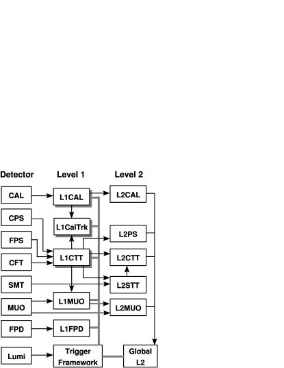
The final stage in the D0 trigger system, Level-3 (L3), consists of a farm of PCs that have access to the full detector readout on L2 accepts. These processors run a simplified version of the offline event reconstruction and make decisions based on physics objects and the relationships between them. L3 accepts events for permanent storage at a rate of up to 150 Hz (typically, 100 Hz).
The configuration of the entire D0 trigger system is accomplished under the direction of the central coordination program (COOR), which is also used for detector configuration and run control.
3 Motivation for the L1Cal Upgrade
By the time of the start of Run IIa in 2001, there was already a tentative plan in place for an extension to the run with accompanying upgrades to the accelerator complex [3], leading to an additional 2–6 fb-1 of integrated luminosity beyond the original goal of 2 fb-1. This large increase in statistical power opens new possibilities for physics at the Tevatron such as greater precision in critical measurements like the top quark mass and W boson mass, the possibility of detecting or excluding very rare Standard Model processes (including production of the Higgs boson), and greater sensitivity for beyond the Standard Model processes like supersymmetry.
At a hadron collider like the Tevatron, however, only a small fraction of the collisions can be recorded, and it is the trigger that dictates what physics processes can be studied and what is left unexplored. The trigger for the D0 experiment in Run IIa had been designed for a maximum luminosity of 11032 cm-2s-1, while the peak luminosities in Run IIb are expected to go as high as 31032 cm-2s-1. In the three-level trigger system employed by D0, only the L3 trigger can be modified to increase its throughput; the maximum output rates at L1 and L2 are imposed by fundamental features of the subdetector electronics. Thus, fitting L1 and L2 triggers into the bandwidth limitations of the system can only be accomplished by increasing their rejection power. While an increase in the transverse energy thresholds at L1 would have been a simple way to achieve higher rejection, such a threshold increase would be too costly in efficiency for the physics processes of interest. For example, raising the thresholds on the two jet triggers used in the search for events to yield acceptable rates would have resulted in a decrease in signal efficiency of more than 20%. The D0 Run IIb Trigger Upgrade [5] was designed to achieve the necessary rate reduction through greater selectivity, particularly at the level of individual L1 trigger elements.
The L1Cal trigger used in Run I and in Run IIa [8] was based on counting individual trigger towers above thresholds in transverse energy (). Because the energy from electrons/photons and especially from jets tends to spread over multiple TTs, the thresholds on tower had to be set low relative to the desired electron or jet . For example, an EM trigger tower threshold of 5 GeV is fully efficient only for electrons with greater than about 10 GeV, and a 5 GeV threshold for EM+HD tower only becomes 90% efficient for jet transverse energies above 50 GeV.
The primary strategy of the Run IIb upgrade of L1Cal is therefore to improve the sharpness of the thresholds for electrons, photons and jets by forming clusters of TTs and comparing the transverse energies of these clusters, rather than individual tower s, to thresholds.
The design of clustering using sliding windows (see Section 4) in Field Programmable Gate Arrays (FPGAs) meets the requirements of this strategy, and also opens new possibilities for L1Cal, including sophisticated use of shower shape and isolation; algorithms to find hadronic decays of tau leptons through their characteristic transverse profile; and requirements on the topology of the electrons, jets, taus, and missing transverse energy in an event.
4 Algorithms for the Run IIb L1Cal
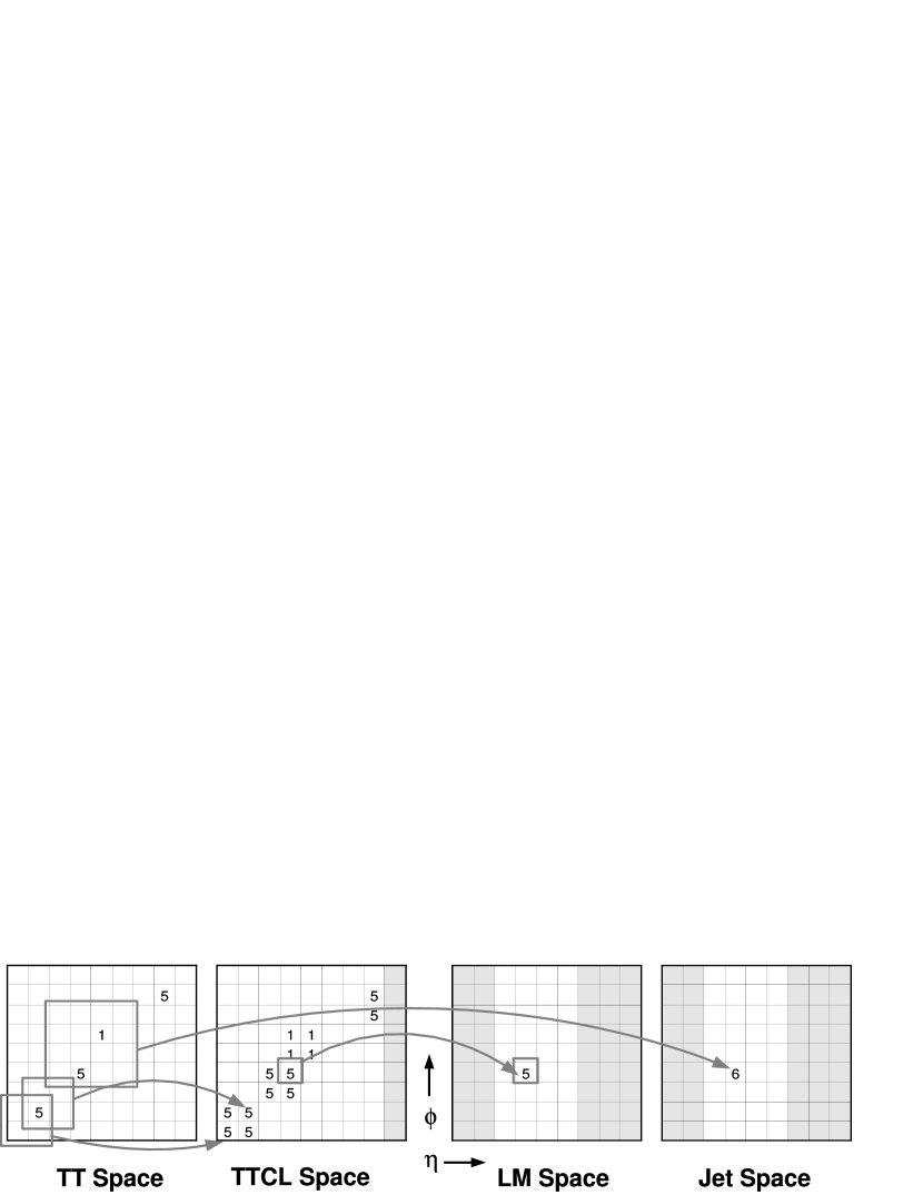
Clustering of individual TTs into EM and Jet objects is accomplished in the Run IIb L1Cal by the use of a sliding windows (SW) algorithm. This algorithm performs a highly parallel cluster search in which groups of contiguous TTs are compared to nearby groups to determine the location of local maxima in deposition. Variants of the SW algorithm have been studied extensively at different HEP experiments [9], and have been found to be highly efficient at triggering on EM and Jet objects, while not having the latency drawbacks of iterative clustering algorithms. For a full discussion of the merits of the sliding windows algorithm, see [10].
The implementation of the sliding windows algorithm in the D0 calorimeter trigger occurs in three phases. In the first phase, the digitized transverse energies of several TTs are summed into Trigger Tower Clusters (TTCL). These TTCL sums, based on the size of the EM or Jet sliding window, are constructed for every point in trigger tower space, and are indexed by the coordinate of one of the contributing TTs, with different conventions being used for different algorithms (see Sections 4.1 and 4.2). This process, which yields a grid of TTCLs that share energy with their close neighbors, is shown in the first and second panels of Fig. 6.
In the second phase, the TTCLs are analyzed to determine locations of large energy deposits called local maxima (LM). These LM are chosen based on a comparison of the magnitude of the of a TTCL with that of its adjacent TTCLs. Multiple counting of Jet or EM objects is avoided by requiring a spatial separation between adjacent local maxima as illustrated in the third panel of Fig. 6.
In the third phase, additional information is added to define an output object. In the case of Jet objects, shown in the fourth panel of Fig. 6, energy of surrounding TTs is added to the TTCL energy to give the total Jet object energy. EM and Tau objects are also refined in this phase using isolation information (see Sections 4.2 and 4.3).
Results for the entire calorimeter can be obtained very quickly using this type of algorithm by performing the LM finding and object refinement phases of the algorithm in parallel for each TTCL.
4.1 Jets
Jets at the Tevatron have lateral sizes of order one unit in space and deposit energy in both the electromagnetic and hadronic portions of the calorimeter. Therefore, Jet objects in the D0 L1Cal are defined using the sum of the EM and HD energies as the input to the TTCL-sums. The TTCLs are 22 in trigger tower units, corresponding to a region 0.40.4 in space on the inner face of the calorimeter. Local maxima are required to be separated by one trigger tower and the final energy sums are 44 in TT space, corresponding to a region 0.80.8 in space.
The values of these clustering parameters were determined by optimizing Jet object energy and position resolution.
4.2 EM Objects
EM objects (electrons or photons) have lateral shower profiles that are much smaller than the TT size, and tend not to deposit energy in the hadronic calorimeter. For this reason, EM TTs are input directly to the local maximum finding algorithm (the TTCL size is 11 in TT units). Because electrons or photons may deposit energy close to the boundary between TTs, the final EM object, as shown in Fig. 7, is comprised of two adjacent trigger towers, oriented horizontally (containing two TTs in ) or vertically (containing two TTs in ), where the first tower is the LM and the second is the neighboring tower with the highest . Cuts can also be applied on the electromagnetic fraction (EM/HD) and isolation of the candidate EM object. The former is determined using the ratio of the EM TT energies making up the EM object and the corresponding two HD TTs directly behind it. The isolation region is composed of the four EM TTs adjacent to the EM object; cuts are placed on the ratio of the total in the EM-isolation region and the EM object . In both cases, the ratio cut value is constrained to be a power of two in order to reduce latency in the divide operation as implemented in digital logic.
This algorithm was chosen based on an optimization of the efficiency for triggering on electrons from and decays.

4.3 Taus
Tau leptons that decay hadronically look similar to jets, but have narrow, energetic cores. This allows extra efficiency for processes containing taus to be obtained by relaxing threshold requirements on these objects (compared to Jet thresholds) but additionally requiring that only small amounts of energy surround the tau candidate. The Run IIb L1Cal uses the results of the Jet algorithm as a basis for Tau objects but also calculates the ratio of the 22 TT TTCL to the 44 total Jet object . Large values of this isolation ratio, as well as large , are required in the definition of a Tau object. Because of data transfer constraints in the system, however, the associated with the Tau object is taken from the Jet object closest in to the LM passing the Tau isolation cut.
4.4 Sum and missing
Scalar and vector sums are computed for the EM+HD TTs. In constructing these sums, the range of the contributing TTs can be restricted and an threshold can be applied to the TTs entering the sums to avoid noise contamination.
4.5 Use of the Intercryostat Detectors
Object and sum energies in the Run IIb L1Cal can be configured to include energies seen in the ICR. Because of complicated calibrations and relatively poor resolution in these regions, however, this option is currently not in use.
4.6 Topological Triggers
Because of its increased processing capabilities, the Run IIb L1Cal can require spatial correlations between some of its objects to create topological trigger terms. These triggers can be used to distinguish signals that have numbers of objects identical to those observed in large backgrounds but whose event topologies are much rarer. An example of such a topology occurs in associated Higgs production in which the decay yields two jets acoplanar with respect to the beam axis, and large missing transverse energy. Since the only visible energy in such an event is reflected in the jets, it is difficult to distinguish this process from the overwhelming dijet QCD background. The Run IIb L1Cal contains a trigger that specifically selects dijet events in which the two jets are required to be acolinear in the transverse plane. Other topological triggers that have been studied are back-to-back (in the transverse plane) EM object triggers to select events containing mesons, and triggers that select events with jet-free regions of the calorimeter containing small energy deposits, for triggering on mono-jet events.
5 Simulation and Predictions
Two independent methods of simulating the performance of the L1Cal algorithms have been developed: a module included in the overall D0 trigger simulation for use with Monte Carlo or real data events (TrigSim), and a tool developed to estimate and extrapolate trigger rates based on real data accumulated during special low-bias runs (Trigger Rate Tool). Both of these methods were used to develop a new Run IIb trigger list that will collect data efficiently up to the highest luminosities foreseen in Run IIb.
5.1 Monte Carlo based Simulation
A C++ simulation of the Run IIb L1Cal trigger has been developed, as part of the full D0 trigger simulation (TrigSim) – a single executable program that provides a standard framework for including code that simulates each individual D0 trigger element. This framework allows the specification of the format of the data transferred between trigger elements, the simulation of the time ordering of the trigger levels and the simulation of the data transfers. The L1Cal portion of TrigSim emulates all aspects of the L1Cal algorithms. It can be run either as part of the full D0 trigger simulation or in a stand-alone mode on both Monte Carlo simulated data and real D0 data, allowing checks on hardware performance, as well as estimates of signal efficiencies and background rates, as part of algorithm optimization.
5.2 Trigger Rate Tool
A great benefit in designing and testing the algorithms for L1Cal in Run IIb was the availability of real collision data from Run IIa. In every event recorded in Run IIa, the transverse energy of every trigger tower was saved. These energies serve as input to a stand-alone emulation of the Run IIb algorithms (the Trigger Rate Tool) used to estimate rates and object-level efficiencies from actual data. Special data runs were taken with low tower thresholds, and the Trigger Rate Tool was applied to these runs to predict the rates for any list of emulated triggers with a proper treatment of the correlations among triggers in the list. The Trigger Rate Tool was also used to compare the Run IIa and Run IIb trigger lists and to extrapolate rates from the relatively low luminosities existing when the Run IIa data was taken to the much higher values anticipated in Run IIb. Predictions based on results obtained from this tool indicated that the upgraded trigger would reduce the overall Level 1 rates by about a factor of two while maintaining equal or improved efficiency for signal processes at the highest instantaneous luminosities foreseen in Run IIb.
5.3 Predictions
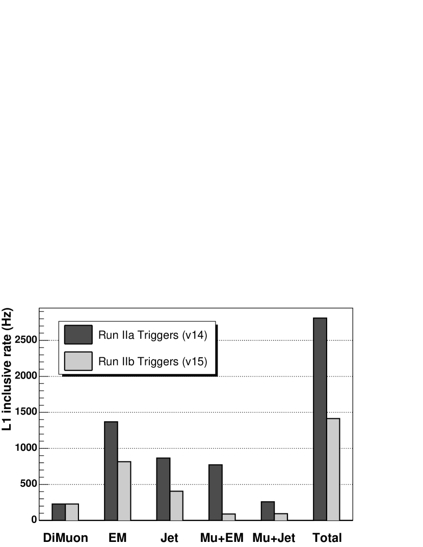
Predictions of the impact of the new L1Cal sliding windows algorithms on the L1 trigger rates and efficiencies were obtained using simulations of dijet events and various physics processes of interest in Run IIb. After trying different configurations that gave the same rate as those experienced during Run IIa, the most efficient configurations were chosen and put in an overall trigger list to check the total rate.
Figure 8 shows the predicted rates at a luminosity of 21032 cm-2s-1, estimated using the Trigger Rate Tool, for trigger lists based on Run IIa algorithms (v14) and their Run IIb equivalents (v15). Both trigger lists were designed to give similar efficiencies for physics objects of interest in Run IIb. However, the Run IIb trigger list yields a rate approximately a factor of two smaller than that achievable using Run IIa algorithms.
6 Hardware Overview
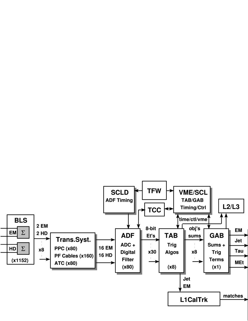
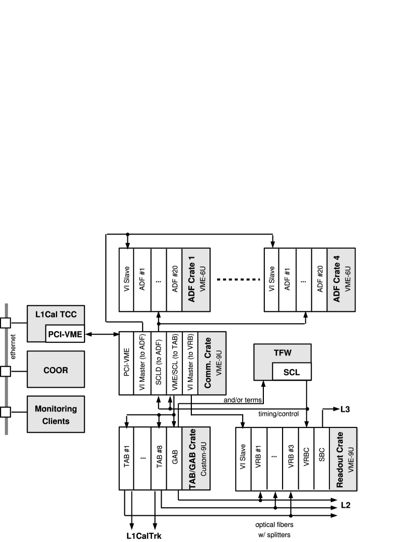
The algorithms described previously are implemented in several custom electronics boards designed for the new L1Cal. An overview of the main hardware elements of the Run IIb L1Cal system is given in Fig. 9. Broadly, these elements are divided into three groups.
-
1.
The ADF System, containing those elements that receive and digitize analog TT signals from the BLS cards, and perform TT-based signal processing.
-
2.
The TAB/GAB System, where algorithms are run on the digitized TT signals to produce trigger terms.
-
3.
The Readout System, which inserts L1Cal information into the D0 data path for permanent storage.
The L1Cal also communicates with other elements of the D0 trigger and data acquisition (DAQ) system, including the following.
-
•
The Trigger Framework (TFW), which delivers trigger decisions and synchronizes the entire D0 DAQ. From the L1Cal point of view, the TFW sends global timing and control signals (see Table 1) to the system over Serial Command Links (SCL) and receives the L1Cal and/or terms.
-
•
The L1Cal Trigger Control Computer (L1Cal TCC), which configures and monitors the system.
-
•
The Level-1 Cal-Track Match trigger system (L1CalTrk), another L1 trigger system that performs azimuthal matching between L1CTT tracks and L1Cal EM and Jet objects.
| SCL | ADF | TAB/GAB | Description |
| INIT | — | yes | initialize the system |
| CLK7 | yes | yes | 132 ns Tevatron RF clock |
| TURN | yes | yes | marks the first crossing of an accelerator turn |
| REALBX | yes | — | flags clock periods containing real beam crossings |
| BX_NO | — | yes | counts the 159 bunch crossings in a turn |
| L1ACCEPT | yes | yes | indicates that an L1 Accept has been issued by the TFW |
| MONITOR | yes | — | initiates collection of ADF monitoring data |
| L1ERROR | — | yes | a TAB/GAB error condition transmitted to the SCL hub |
| L1BUSY | — | yes | asserted by the TABs/GAB until an observed error is cleared |
| — | ADF_MON | — | allows TCC to freeze ADF circular buffers |
| — | ADF_TRIG | — | allows TCC to fake a MONITOR signal on the next L1 Accept |
| — | — | TAB_RUN | TAB/GAB data path synchronization signal |
| — | — | TAB_TRIG | pulse to force writing to TAB/GAB diagnostic memories |
| — | — | TAB_FRM | used for synchronization of TAB/GAB VME data under VME/SCL control |
| — | — | TAB_ADDR | internal address for TAB/GAB VME read/write operations |
| — | — | TAB_DATA | data for TAB/GAB VME read/write operations |
Within the L1Cal, the ADF system consists of the Transition System, the Analog and Digital Filter cards (ADF), and the Serial Command Link Distributor (SCLD). The Transition System, consisting of Patch Panels, Patch Panel Cards (PPC), ADF Transition Cards (ATC), and connecting cables, adapts the incoming BLS signal cables to the higher density required by the ADFs. These ADF cards, which reside in four 6U VME-64x crates [11], filter, digitize and process individual TT signals, forming the building blocks of all further algorithms. They receive timing and control signals from the SCL via a Serial Command Link Distributor card (SCLD).
Trigger algorithms are implemented in the L1Cal in two sets of cards: the Trigger Algorithm Boards (TAB) and the Global Algorithm Board (GAB), which are housed in a single 9U crate with a custom backplane. The TABs identify EM, Jet and Tau objects in specific regions of the calorimeter using the algorithms described in Section 4 and also calculate partial global energy sums. The GAB uses these objects and energy sums to calculate and/or terms, which the TFW uses to make trigger decisions. Finally, the VME/SCL card, located in the L1Cal Control Crate, distributes timing and control signals to the TABs and GAB and provides a communication path for their readout.
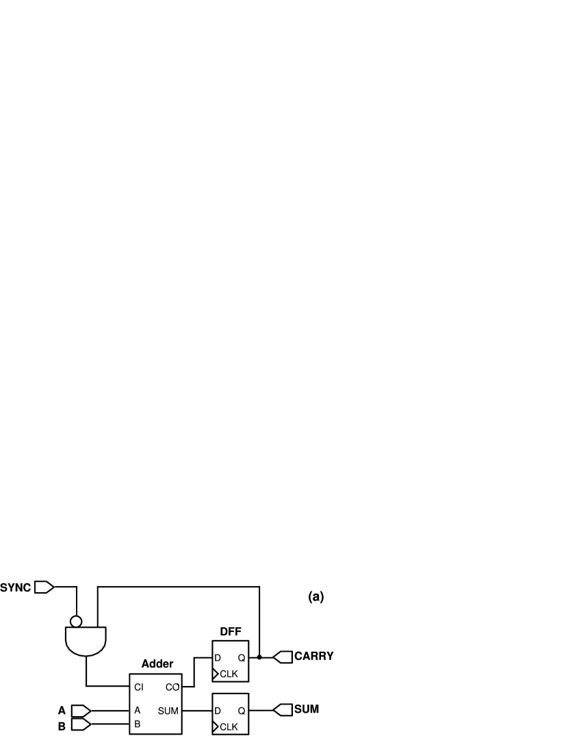
The architecture of the L1Cal system and the number of custom elements required, summarized in Table 2, is driven by the large amount of overlapping data required by the sliding windows algorithm. In total, more than 700 Gbits of data per second are transmitted within the system. Of this, each local maximum calculation requires 4.4 Gbits/s from 72 separate TTs. The most cost effective solution to this problem, which still results in acceptable trigger decision latency, is to deal with all data as serial bit-streams. Thus, all intra-system data transmission is done bit-serially using the Low Voltage Differential Signal (LVDS) protocol and nearly all algorithm arithmetic is performed bit-serially as well, at clock speeds such that all bits of a data word are examined in the 132 ns Tevatron bunch crossing interval. Examples of a bit-serial adder and comparator are shown in Fig. 10. The only exception to this bit-serial arithmetic rule is in the calculation of Tau object isolation, which requires a true divide operation (see Section 4) and thus introduces an extra 132 ns of latency to the trigger term calculation. Even with this extra latency, the L1Cal results arrive at the TFW well within the global L1 decision time budget.
| Board | Input TT Region | Output TT Region | Total Number |
| PPC | 44 | 44 | 80 |
| ATC | 44 | 44 | 80 |
| ADF | 44 | 44 | 80 |
| SCLD | all | all | 1 |
| TAB | 4012 | 314 | 8 |
| GAB | all | all | 1 |
| VME/SCL | all | all | 1 |

7 The ADF System
7.1 Transition System
Trigger pick-off signals from the BLS cards of the EM and HD calorimeters are transmitted to the L1Cal trigger system, located in the Movable Counting House (MCH), through 40–50 m long coaxial ribbon cables. Four adjacent coaxial cables in a ribbon carry the differential signals from the EM and HD components of a single TT. Since there are 1280 BLS trigger cables distributed among ten racks of the original L1Cal trigger electronics, the L1Cal upgrade was constrained to reuse these cables. However, because the ADF input signal density is much larger than that in the old system (only four crates are used to house the ADFs as opposed to 10 racks for the old system’s electronics) the cables could not be plugged directly into the upgraded L1Cal trigger electronics; a transition system was needed.
The transition system is composed of passive electronics cards and cables that route signals from the BLS trigger cables to the backplane of the ADF crates (see Section 7.2). It was designed to allow the trigger cables to remain within the same Run I/IIa rack locations. It consists of the following elements.
-
•
Patch Panels and Patch Panel Cards (PPC): A PPC receives the input signals from 16 BLS trigger cables and transmits the output through a pair of Pleated Foil Cables. A PPC also contains four connectors which allow the monitoring of the signals. Eight PPCs are mounted two to a Patch Panel in each of the 10 racks originally used for Run I/IIa L1Cal electronics.
-
•
Pleated Foil Cables: Three meter long Pleated Foil Shielded Cables (PFC), made by the 3M corporation [12], are used to transfer the analog TT output signals from the PPC to the ADF cards via the ADF Transition Card. There are two PFCs for each PPC for a total of 160 cables. The unbalanced characteristic impedance specification of the PFC is 72 , which provides a good impedance match to the BLS trigger cables.
-
•
ADF Transition Card (ATC): The ATCs are passive cards connected to the ADF crate backplane. These cards receive the analog TT signals from two PFCs and transmit them to the ADF card. There are 80 ATCs that correspond to the 80 ADF cards. Each ATC also transmits the three output LVDS cables of an ADF card to the TAB crate – a total of 240 LVDS cables.
7.2 ADF Cards
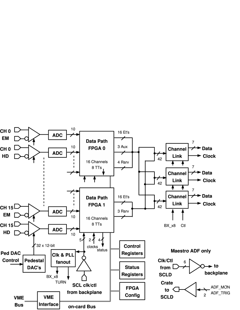
The Analog and Digital Filter cards (ADF) are responsible for sending the best estimate of the transverse energy () in the EM and HD sections of each of the 1280 TTs to the eight TAB cards for each Tevatron beam crossing. The calculation of these values by the 80 ADF cards is based upon the 2560 analog trigger signals that the ADF cards receive from the BLS cards, and upon the timing and control signals that are distributed throughout the D0 data acquisition system by the Serial Command Links (SCL). The ADF cards themselves are 6U 160 mm, 12-layer boards designed to connect to a VME64x backplane using P0, P1 and P2 connectors. The ADF system is set up and monitored, over VME, by a Trigger Control Computer (TCC), described in Section 10.
7.3 Signal Processing in the ADFs
Each ADF card, as shown schematically in Fig. 11, uses 32 analog trigger signals corresponding to the EM and HD components of a 44 array of Trigger Towers. Each differential, AC coupled analog trigger signal is received by a passive circuit that terminates and compensates for some of the characteristics of the long cable that brought the signal out of the collision hall. Following this passive circuit the active part of the analog receiver circuit rejects common mode noise on the differential trigger signal, provides filtering to select the frequency range of the signal caused by a real Tevatron energy deposit in the Calorimeter, and provides additional scaling and a level shift to match the subsequent ADC circuit.
The analog level shift in the trigger signal receiver circuit is controlled, separately for each of the 32 channels on an ADF card, by a 12 bit pedestal control DAC, which can swing the output of the ADC that follows it from slightly below zero to approximately the middle of its full range. This DAC is used both to set the pedestal of the signal coming out of the ADC that follows the receiver circuit and as an independent way to test the full signal path on the ADF card. During normal operation, we set the pedestal at the ADC output to 50 counts which is a little less than 5% of its full scale range. This offset allows us to accommodate negative fluctuations in the response of the BLS circuit to a zero-energy signal.
The 10 bit sampling ADCs [13] that follow the receiver circuit make conversions every 33 ns – four times faster than the Tevatron BX period of 132 ns. This conversion rate is used to reduce the latency going through the pipeline ADCs and to provide the raw data necessary to associate the rather slow rise-time trigger signals (250 ns typical rise-time) with the correct Tevatron beam crossing. Although associating energy deposits in the Calorimeter with the correct beam crossing is not currently an issue since actual proton-antiproton collisions only occur every 396 ns, rather than every 132 ns as originally planned, the oversampling feature has been retained for the flexibility it provides in digital filtering.
On each ADF card the 10 bit outputs from the 32 ADCs flow into a pair of FPGAs [14], called the Data Path FPGAs, where the bulk of the signal processing takes place. This signal processing task, shown schematically in Fig. 12, is split over two FPGAs with each FPGA handling all of the steps in the signal processing for 16 channels. Two FPGAs were used because it simplified the circuit board layout and provided an economical way to obtain the required number of I/O pins.

The first step in the signal processing is to align in time all of the 2560 trigger signals. The peak of the trigger signals from a given beam crossing arrive at the L1Cal at different times because of different cable lengths and different channel capacitances. These signals are made isochronous using variable length shift registers that can be set individually for each channel by the TCC. Once the trigger signals have been aligned in time, they are sent to both the Raw ADC Data Circular Buffers where monitoring data are recorded and to the input of the Digital Filter stage.
The Raw ADC Data Circular Buffers are typically set up to record all 636 of the ADC samples registered in a full turn of the accelerator. This writing operation can be stopped by a signal from the TCC, when an L1 Accept flagged with a special Collect Status flag is received by the system on the SCL, or in a self-trigger mode where any TT above a programmable threshold causes writing of all Circular Buffers to stop. Once writing has stopped, all data in the buffers can be read out using the TCC, providing valuable monitoring information on the system’s input signals. The Raw ADC Data Circular Buffers can also be loaded by the TCC with simulated data, which can be inserted into the ADF data path instead of real signals for testing purposes.
The Digital Filter in the signal processing path can be used to remove high frequency noise from the trigger signals and to remove low frequency shifts in the baseline. This filter is currently configured to select the ADC sample at the peak of each analog TT signal. This mode of operation allows the most direct comparison with data taken with the previous L1Cal and appears to be adequate for the physics goals of the experiment.
The 10 bit output from the Digital Filter stage has the same scale and offset as the output from the ADCs. It is used as an address to an E to Lookup Memory, the output of which is an eight bit data word corresponding to the seen in that TT. This to conversion is normally programmed such that one output count corresponds to 0.25 GeV of and includes an eight count pedestal, corresponding to zero from that TT.
The eight bit TT is one of four sources of data that can be sent from the ADF to the TABs under control of a multiplexer (on a channel by channel and cycle by cycle basis). The other three multiplexer inputs are a fixed eight-bit value read from a programmable register, simulation data from the Output Data Circular Buffer, and data from a pseudo-random number generator.
The latter two of these sources are used for system testing purposes. During normal operation, the multiplexers are set up such that TT data are sent to the TABs on those bunch crossing corresponding to real proton-antiproton collisions, while the fixed pedestal value (eight counts) is sent on all other accelerator clock periods. If noise on a channel reaches a level where it significantly impacts the D0 trigger rate, then this channel can be disabled, until the problem can be resolved, by forcing it to send the fixed pedestal on all accelerator clock periods, regardless of whether they contain a real crossing or not. Typically, less than 10 (of 2560) TTs are excluded in this manner at any time.
Data are sent from the ADF system to the TAB cards using a National Semiconductor Channel Link chip set with LVDS signal levels between the transmitter and receiver [15]. Each Channel Link output from an ADF card carries the data for all 32 channels serviced by that card. A new frame of data is sent every 132 ns. All 80 ADF cards begin sending their frame of data for a given Tevatron beam crossing at the same point in time. Each ADF card sends out three identical copies of its data to three separate TABs, accommodating the data sharing requirements of the sliding windows algorithm.
7.4 Timing and Control in the ADF System
The ADF system receives timing and control signals listed in Table 1 over one of the SCLs [2]. Distribution of these signals from the SCL to the 80 ADF cards is accomplished by the SCL Distributor (SCLD) card. The SCLD card receives a copy of the SCL information using a D0-standard SCL Receiver mezzanine card and fans out the signals mentioned in Table 1 to the four VME-64x crates that hold the 80 ADF cards using LVDS level signals. In addition, each ADF crate sends two LVDS level signals (ADF_MON and ADF_TRIG) back to the SCLD card, allowing the TCC to cause synchronous readout of the ADFs.
Within an ADF crate, the ADF card at the mid-point of the backplane (referred to as the Maestro) receives the SCLD signals and places them onto spare, bused VME-64x backplane lines at TTL open collector signal levels. All 20 of the ADF cards in a crate pick up their timing and control signals from these backplane lines. To ensure a clean clock, the CLK7 signal is sent differentially across the backplane and is used as the reference for a PLL on the ADFs. This PLL provides the jitter-free clock signal needed for LVDS data transmission to the TABs and for ADC sampling timing.
7.5 Configuring and Programming the ADF System
The ADF cards are controlled over a VME bus using a VME-slave interface implemented in a PAL that is automatically configured at power-up. Once the VME interface is running, the TCC simultaneously loads identical logic files into the two data path FPGAs on each card. Since each data path FPGA uses slightly different logic (e.g., the output check sum generation), the FPGA flavor is chosen by a single ID pin. After TCC has configured all of the data path FPGAs, it then programs all control-status registers and memory blocks in the ADFs. Information that is held on the ADF cards that is critical to their physics triggering operation is protected by making those programmable features “read only” during normal operation. TCC must explicitly unlock the write access to these features to change their control values. In this way no single failed or mis-addressed VME cycle can overwrite these critical data.
8 ADF to TAB Data Transfer
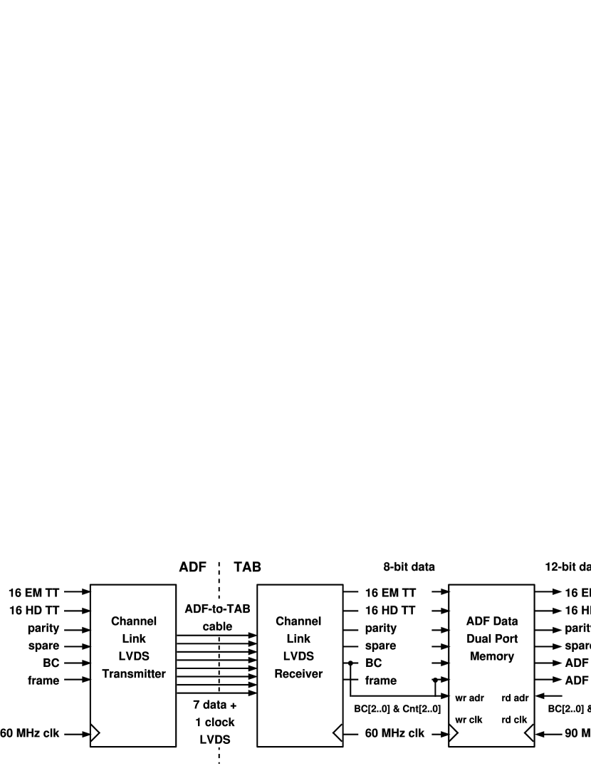
Digitized TT data from each ADF’s 44, region are sent to the TABs for further processing, as shown in Fig. 13. To accommodate the high density of input on the TABs, the 8-bit serial trigger-tower data are transmitted using the channel-link LVDS chipset [15], which serializes 48 CMOS/TTL inputs and the transmission clock onto seven LVDS channels plus a clock channel. In the L1Cal system, the input to the transmitter is 60 MHz TTL (eight times the bunch crossing rate), which is stepped up to 420 MHz for LVDS transmission.
Each ADF sends three identical copies of 36 8-bit words to three different TABs on each bunch crossing. This data transmission uses eight LVDS channels – seven data channels containing six serialized data words each, and one clock – on Gore cables with 2mm HM connectors [16]. The 36 data words consist of the digitized of 16 EM and 16 HD TTs and four control words. The bunch crossing number control word indicates which accelerator crossing produced the ADF data being transmitted, and is used throughout the system for synchronization. The frame-bit control word is used to help align the least significant bits of the other data words. The parity control word is the logical XOR of every other word and is used to check the integrity of the data transmission. Finally, one control word is reserved for future use.
While the ADF logic is 8-bit serial (60 MHz) the TAB logic is 12-bit serial (90 MHz). To cross the clock domains, the data passes through a dual-port memory with the upper four bits padded with zeros. The additional bit space is required to accommodate the sliding windows algorithm sums.
The dual port memory write address is calculated from the frame and bunch crossing words of the ADF data. The least significant address bits are a data word bit count, which is reset by the frame signal, while the most significant address bits are the first three-bits of the bunch crossing number. This means that the memory is large enough to contain eight events of eight-bit serial data.
By calculating the read address in the same fashion, but from the TAB frame and bunch crossing words, the dual-port memory crosses 60 MHz/90 MHz clock domains, maintains the correct phase of the data, and synchronizes the data to within eight crossings all at the same time. This means the TAB timing can range between a minimal latency setting where the data are retrieved just after they are written and a maximal latency setting where the data are retrieved just before they are overwritten. If the TAB timing is outside this range, the data from eight previous or following crossings will be retrieved.
Although off-the-shelf components were used within their specifications, operating 240 such links reliably was found to be challenging. Several techniques were employed to stabilize the data transmission. Different cable lengths (between 2.5 and 5.0 m) were used to match the different distances between ADF crates and the TAB/GAB crate. The DC-balance and pre-emphasis features of the channel-link chipset [15] were also used, but deskewing, which was found to be unreliable, was not.
9 The TAB/GAB System
9.1 Trigger Algorithm Board
The Trigger Algorithm Boards (TABs) find EM, Jet and Tau candidates using the sliding windows algorithm and perform preliminary sums for total and missing calculations. Each TAB is a double-wide 9U 400 mm, 12-layer card designed for a custom backplane. The main functional elements of the TAB are shown in Fig. 14.
In the TAB’s main trigger data path, LVDS cables from 30 ADFs are received at the back of the card using feedthrough connectors on the backplane. The data from these cables are extracted using Channel Link receivers[15] and sent, as individual bit-streams for each TT, to ten TAB sliding windows algorithm (SWA) FPGAs [17] for processing. These chips also pass some of their data to their nearest neighbors to accommodate the data sharing requirements of the sliding windows algorithms. The algorithm output from each SWA is sent to a single TAB global FPGA [17]. The global FPGA calculates regional sums and sends the results out the front of the board to the GAB, over the same type of cables used for ADF to TAB data transmission (see Section 8) using embedded LVDS functionality in the FPGA. This data transmission occurs at a clock rate of 636 MHz.
The global FPGA also sends three copies of Jet and EM object information for each bunch crossing to the L1CalTrk system for processing using Gbit/s serial link transmitter daughter cards (MUON SLDB) [2]. Upon receiving an L1 accept from the D0 TFW, the TAB global chip also sends data out on a serial fiber-optic link [18] for use by the L2 trigger and for inclusion in the D0 event data written to permanent storage on an L3 accept.
Low-level board services are provided by the TAB Cyclone chip [19], which is configured by an on-board serial configuration device [20] on TAB power-up. These services include providing the path for power-up and configuration of the other FPGAs on the board, under the direction of the VME/SCL card; communicating with VME and the D0 SCL over the specialized VME/SCL serial link; and fanning out the 132 ns detector clock using an on-board clock distribution device [21].
9.2 Global Algorithm Board

The global algorithm board (GAB) receives data containing regional counts of Jet, EM, and Tau physics objects calculated by the TABs and produces a menu of and/or terms, which is sent to the D0 trigger framework. Like the TAB, the GAB is a double-wide 9U 400 mm, 12-layer circuit board designed for a custom backplane. Its main functional elements are shown in Fig. 15.
LVDS receivers, embedded in four Altera Stratix FPGAs (LVDS FPGAs) [17] each receive the output of two TABs, synchronizing the data to the GAB 90 MHz clock using a dual-port memory. The synchronized TAB data from all four LVDS FPGAs is sent to a single GAB S30 FPGA [17], which calculates and/or terms, and sends them to the trigger framework through TTL-to-ECL converters [22]. There are five 16-bit outputs on the GAB, although only four are used by the framework.
9.3 VME/SCL Board and the TAB/GAB Control Path
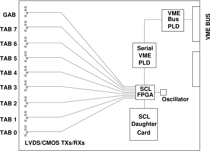
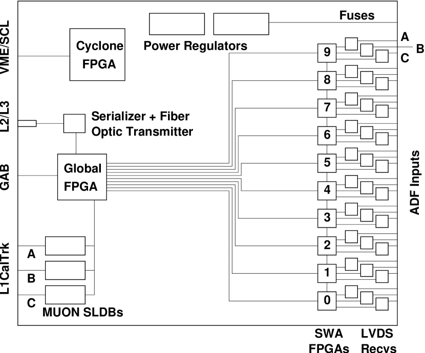
Because of the high-density of inputs to the TAB and GAB modules, direct connections of these cards to a VME bus is impossible. A custom control path for these boards is provided by the VME/SCL module, a double-wide 9U 400 mm, 8-layer board. A block diagram of the main elements of this card can be found in Fig. 16. SCL signals arrive at the VME/SCL board via an SCL receiver daughter card and those signals used by the TAB/GAB system are selected for fanout by the SCL FPGA [25], which also handles transmission/reception of serialized VME communications with the TABs and GAB. Any VME communication, directed to (from) a card in the TAB/GAB system, is received by (transmitted from) the VME Bus PLD, which implements the VME protocol. Those commands whose destination (source) is one of the TAB or GAB boards are translated to (from) the custom serial protocol listed in Table 1 by the Serial VME PLD, which connects to the SCL FPGA for signal transmission (reception). Serial communications between the VME/SCL card and the TABs and GAB is accomplished using LVDS protocol [23], on nine cables – one for each TAB and GAB.
9.4 TAB/GAB Trigger Data Path
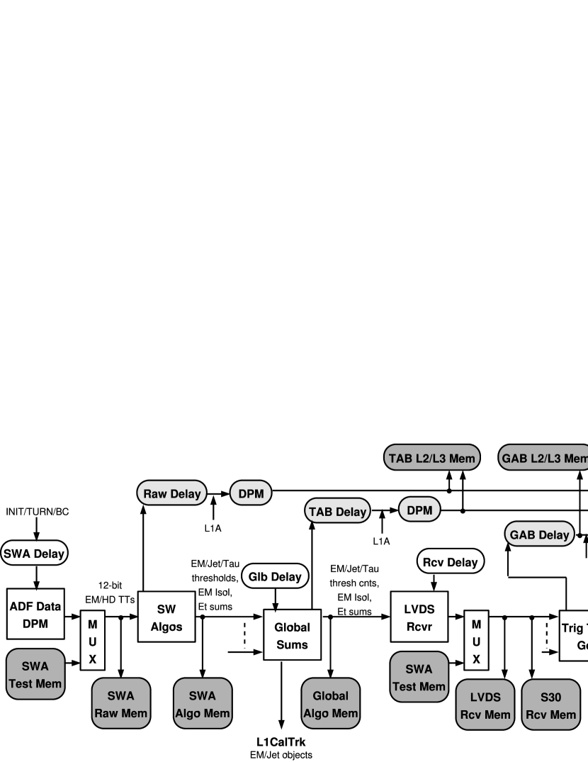
The path of trigger data through the TAB/GAB system is shown in Fig. 17. Each of the eight TABs receives data from 30 ADF cards, covering a 4012 region in space. Eight-bit TT data are translated to 12-bit words in the ADF Data DPM and are transmitted serially to the SWA FPGAs where EM, Jet and Tau objects are found. Each of the ten TAB SWA chips finds objects in a 44, grid, for which it requires a 99 region of input TTs. This TT data comes from the three LVDS receivers (A,B,C in Fig. 14) attached directly to the chip and also, indirectly, from its nearest neighbor SWA chips. A map of the TT inputs to a single SWA chip is given in Table 3. In this table and the following discussion, we use global indices ( and ) when referring to the entire grid but switch to local indices ([2,6] and [2,6]) for single SWA chips. The translation between the two systems is given below.
| (1) |
Note that data for indices 0, 1, 38, and 39, at all positions, correspond to signals from the ICR detectors, which can be added to the relevant calorimeter TTs if desired.
| cable: | C | B | A | chip | ||||||
| / | 2 | 1 | 0 | 1 | 2 | 3 | 4 | 5 | 6 | |
| 6 | 72 | 73 | 74 | 75 | 76 | 77 | 78 | 79 | 80 | |
| 5 | 63 | 64 | 65 | 66 | 67 | 68 | 69 | 70 | 71 | SWA 1 |
| 4 | 54 | 55 | 56 | 57 | 58 | 59 | 60 | 61 | 62 | |
| 3 | 45 | 46 | 47 | 48 | 49 | 50 | 51 | 52 | 53 | |
| 2 | 36 | 37 | 38 | 39 | 40 | 41 | 42 | 43 | 44 | SWA |
| 1 | 27 | 28 | 29 | 30 | 31 | 32 | 33 | 34 | 35 | |
| 0 | 18 | 19 | 20 | 21 | 22 | 23 | 24 | 25 | 26 | |
| 1 | 9 | 10 | 11 | 12 | 13 | 14 | 15 | 16 | 17 | SWA 1 |
| 2 | 0 | 1 | 2 | 3 | 4 | 5 | 6 | 7 | 8 | |
Each SWA chip sends the results of its algorithms to the Global Chip as 12-bit serial data on 25 lines. The data transmitted consists of the following.
-
•
The highest of seven possible thresholds passed by EM and Jet objects at each of the 44, positions considered by this chip, or zero if the object is below all thresholds. This information (three bits for each position and object) is packed into a total of eight, 12-bit words, with each word containing data from the four locations at a specific for one object type.
-
•
The highest of seven possible Tau isolation ratio thresholds (see Section 4.3) passed by Tau objects at each of the 44, positions considered by this chip, or zero if the ratio is below all thresholds. This information is packed in the same way as the EM and Jet object data above.
-
•
The results of the EM isolation and EM fraction calculations (see Section 4.2) for each of the 44 locations considered in this chip. A single bit, corresponding to a specific , location is set if the EM object at that location passes both the EM isolation and EM fraction cuts.
-
•
Sums over four locations of EM+HD for each position considered in this chip.
-
•
Four-bit counts of the number of TTs in the chip with EM+HD greater than three programmable thresholds. This information is used to aid in the identification of noisy channels.
-
•
Raw TT ’s for transmission to the L2 and L3 systems (only transmitted on those BCs marked as L1ACCEPT).
-
•
The bunch crossing number and a flag indicating if there was a bunch crossing number mismatch between the ADF data and the TAB’s local BX .
-
•
Status information.
-
•
Two spare lines.
The Global Chip receives these data from the ten SWA Chips and constructs object counts in a 314 region, as well as sums. The reduced number of positions available for TAB object output comes from edge effects in the sliding windows algorithms and from the use of TTs at indices 0, 1, 38, and 39 for ICR energies. The TABs further concentrate their data by summing object counts in three ranges – North (N), Central (C), and South (S) [24] – before sending their results to the GAB.
A total of 48 12-bit data words are transmitted from each TAB to the GAB. These data include the following.
-
•
Two-bit counts of the number of EM and Jet objects over each of six possible thresholds in the N, C, and S regions for each of the four positions considered by the TAB. Each 12-bit word contains counts for all six thresholds for a specific object in an region and position.
-
•
Two-bit counts of the number of Tau objects over each of six possible Tau ratio thresholds in the same format as the EM and Jet information above.
-
•
Single bits indicating that at least one EM object passed the isolation criteria in an region (S,C,N) at a specific position. Since not enough data lines were available to transmit isolation information for each possible EM object, this grouping represents a compromise that allows the GAB to construct isolated EM triggers if any EM object in an region is found to be isolated.
-
•
Sums of EM+HD , , and scalar over the 404 region belonging to the TAB. and are calculated using sine and cosine look-ups appropriate for each TT’s position.
-
•
Eight-bit counts of the number of TTs with EM+HD greater than three thresholds.
-
•
Bunch Crossing, status, synchronization and parity information.
At the GAB, TAB data are received and transmitted unchanged to the S30 Chip where and/or trigger terms are constructed as described in Section 13.1. A total of 64 and/or terms are sent from the GAB to the Trigger Framework.
9.5 TAB/GAB Timing and Readout
The timing and readout of the TAB and GAB modules, shown in Fig. 17, are interrelated. Both data traveling on the trigger path and on the readout path to the L2 and L3 systems on L1ACCEPT must be synchronized so that they correspond to a single, known bunch crossing number. This synchronization is accomplished by setting adjustable Delay FIFOs in the TABs and GAB such that the BX_NO stamp on the data at each stage in processing corresponds to the BX_NO being transmitted to the TAB/GAB system by the VME/SCL card. Errors are stored in status registers if a mismatch between these numbers is detected at any point in the chain.
Readout of TAB/GAB data for further processing in the L2 and L3 trigger systems is accomplished by storing data, at various stages of the processing, in pipelines (Raw Delay, TAB Delay, and GAB Delay), whose depth is adjusted so that the data appears at the end of the pipeline when the L1 trigger decision arrives at the boards. If the decision is L1ACCEPT, then the relevant data are moved to Dual Port Memory buffers for transmission, via optical fiber, to the L2 and L3 systems.
Identical data are sent to L2 and L3 by optically splitting the output signals. These data consist of the following:
-
•
The raw eight-bit EM and EM+HD values for each TT (Raw).
-
•
A bit-mask with each bit corresponding to a possible EM, Jet or Tau object either set or not depending on whether the object has passed a L2 threshold (TAB).
-
•
The set of 64 and/or terms transmitted from the GAB and the total , , and sums (GAB).
-
•
A set of control, status and data integrity checksum words.
9.6 TAB/GAB data to L1CalTrk
The L1CalTrk system receives EM and Jet object data for each position from the TAB Global Chips [26]. Each TAB sends three identical copies of its data (to eliminate cracks in the acceptance) to the L1CalTrk system using three Muon Serial Link Daughter cards. These daughter cards serialize seven 16-bit words per bunch crossing period and transmit them to Muon Serial Link Receiver Daughter cards in the L1CalTrk electronics. Four of these words contain EM and Jet information for each of the regions considered by the TAB. Each word is broken into seven-bit EM and Jet parts, where bit is set in each part if any object of that type above threshold is found in the full range. A parity word and two spare words are also transmitted.
9.7 TAB/GAB diagnostic memories
The TAB and GAB modules have a series of VME-readable diagnostic memories (see Fig. 17) designed to capture data from each step of the algorithm calculation. Their contents are snapshots of data transfered between elements of the TAB/GAB system and are generally capable of holding data for 32 consecutive bunch crossing periods, although the L2/L3 Memories and the S30 Trig Memory are limited to one event’s worth of data. These memories are normally written when a TAB_TRIG signal is sent from the VME/SCL board under user control. Both the TABs and GAB also have VME-writable test input memories, which allow arbitrary patterns to be used in the place of the incoming data from the ADF or TAB cards.
10 Online Control
Most components of the D0 trigger and data acquisition system are programmable. The Online System allows this large set of resources and parameters to be configured to support diverse operational modes – broadly speaking, those used during proton-antiproton collisions in the Tevatron (physics modes) and those used in the absence of colliding beams (calibration/testing modes), forming a large set of resources and parameters needing to be configured before collecting data.
The L1Cal fits seamlessly into this Online System, with its online control software hiding the complexity of the underlying hardware, while making the run time programming of the L1Cal Trigger accessible to all D0 users in simple and logical terms. A diagram of the L1Cal, from an online data and control point of view, is shown in Fig. 18. The main elements of L1Cal online control are listed below, with those aspects specific to L1Cal described in more detail in the following sections. For more information on D0-wide components see [2].
-
•
The Trigger Framework (TFW) delivers global D0 timing and control signals to the L1Cal and collects and/or terms from the GAB as described in Section 6.
-
•
COOR [2], a central D0 application, coordinates all trigger configuration and programming requests. Global trigger lists, containing requirements and parameters for all triggers used by the experiment, are specified using this application as are more specific trigger configurations (several of which may operate simultaneously) used for calibration and testing.
-
•
The L1Cal Trigger Control Computer (TCC), a PC running the Linux operating system, provides a high level interface between COOR and the L1Cal hardware and allows independent expert control of the system.
-
•
The Communication Crate contains cards that provide an interface between the L1Cal custom hardware in the ADF and TAB/GAB crates, and the L1Cal TCC and SCL.
-
•
The L1Cal Readout Crate allows transmission of L1Cal data to the L3 trigger system.
-
•
Monitoring Clients, consisting of software that may run on a number of local or remote computers, display information useful for tracking L1Cal operational status.
10.1 L1Cal Control Path
The L1Cal Trigger Control Computer needs to access the 80 ADF cards in their four 6U VME crates; the eight TAB and one GAB cards in one 9U custom crate; and the readout support cards in one 9U VME crate. It uses a commercial interface to the VME bus architecture – the model 618 PCI-VME bus adapter [27]. This adapter consists of one PCI module located in the TCC PC and one VME card located in the Communication Crate, linked by an optical cable pair.
To access the four ADF crates, the L1Cal system uses a set of Vertical Interconnect (VI) modules built by Fermilab [28]. One VI Master Card is located in the Communication Crate, and is connected to four VI Slaves, one in each ADF Crate. The VI Master maps the VME A24 address space of each remote ADF crate onto four contiguous segments of VME A32 addresses in the Communication Crate. User software running on the L1Cal TCC generates VME A32/D16 cycles in the Communication Crate, and A24/D16 in the ADF crate, via the VI Master-Slave interface. The Communication crate also hosts one additional VI Master to access a VI Slave located in the L1Cal Readout Crate.
As discussed in Section 9.3, VME transactions with the TAB/GAB crate are accomplished via the VME/SCL card, housed in the Communication Crate. User software running on L1Cal TCC generates VME A24/D32 cycles to the VME/SCL, which in turn generates a serialized transaction directly to the targeted TAB or GAB module.
10.2 L1Cal Control Software
The functionality required from the control software on the L1Cal TCC is defined by three interfaces: the COOR Interface, the L1Cal Expert Interface, and the Monitoring Interface. The first two of these are used to configure and control L1Cal operations globally (COOR) or locally when performing tests (Expert). The Monitoring Interface collects monitoring information from the hardware for use by Monitoring Clients (see Section 11).
The L1Cal online code itself is divided into two parts: the Trigger Control Software (TCS), written in C++ and C, where the main functionality of the above three interfaces is implemented; and the L1Cal Graphical User Interface (GUI), written in Python [29] with TkInter [30], which allows experts to interact directly with the TCS.
While the GUI normally runs on the L1Cal TCC computer, it can also be launched from a different computer located at D0 or at a remote institution. Since it is a non-critical part of the control software, the GUI does not need to run all the time, but several instances of it can be started and stopped as desired, independently from the TCS. Once started, an instance of the GUI communicates with the TCS by exchanging XML (Extensible Markup Language) [31] text strings.
For communications across each of its three interfaces the TCS uses the ITC (Inter Task Communication) package developed by D0 and based on the open-source ACE (Adaptive Communication Environment) software [32]. ITC provides high level management of client-server connections where communication between separate processes, which may be running on separate computers, is dynamically buffered in message queues. The TCS uses ITC to: receive text commands from COOR and send acknowledgments back with the command completion status; receive XML string commands from the GUI application and send XML strings back to the GUI; and receive fixed format binary monitoring requests from the monitoring clients and send the requested fixed format binary block of data.
10.3 Main Control Operations
Control operations in the L1Cal online software fall into three main categories: configuration, initialization and run-time programming. Configuration consists of loading pre-synthesized firmware into all the FPGAs in the system. Initialization then brings the system into a well-defined idle state. During initialization, all control registers, geometric constants, lookup tables, calibration parameters, etc. are overwritten with their desired values. It is also at this stage that problematic TTs are excluded from consideration by programming their corresponding ADF cards to always report zero for the TTs in question. The most IO intensive part of the initialization is in the programming and verification of the 2,560 ADF Lookup Memories, which takes approximately five seconds. After initialization, COOR performs the run time programming step, where the specific meaning of each L1Cal trigger output signal (the and/or terms) is defined. This involves loading threshold values and other algorithm parameters into the TABs as well as associating combinations of objects and selection criteria in the GAB with individual output and/or bits. Once these tasks have been accomplished, the system runs largely without external intervention, except for monitoring data collection.
11 Managing Monitoring Information
The monitoring resources available in the ADF, TAB and GAB cards are described in Sections 7.3 and 9.7. This information is collected by the TCC Control Software and is made available to Monitoring Clients via the Monitoring Interface as outlined in Section 10.2. During normal operation, monitoring data are collected approximately every five seconds when the Collect Status qualifier is asserted on the SCL along with L1ACCEPT. If data flow has stopped, monitoring data are still collected from the L1Cal, initiated by the TCS, which times out after six seconds of inactivity.
Monitored data include the following.
-
•
The ADF output of all TTs for all 36 active bunch crossings of the accelerator turn containing the L1ACCEPT for which the Collect Status signal is asserted.
-
•
The bunch crossing number within this turn that identifies the L1ACCEPT.
-
•
The contents of all error and status registers in the TABs and GAB (associated with each SWA and Global chip on the TABs and with the LVDS and S30 chips on the GAB). These registers indicate, among other information, synchronization errors on data transfer links, parity errors on each transfer, and bunch crossing number mismatches at various points in the TAB/GAB signal processing chain.
Monitoring information is displayed in the D0 control room and remotely using Monitoring Client GUIs. This application, written in Python [29] with Tkinter [30], requests and receives data from the TCS via calls to ITC. It displays average pedestal values and RMSs for each TT, to aid in the identification of noisy or dead channels, as well as system status information.
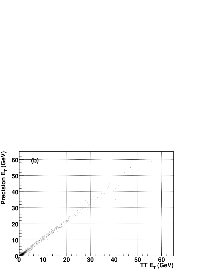
Another tool for monitoring data quality in the control room is a suite of ROOT-based [33] software packages called Examine. The L1Cal Examine package receives a stream of data from L3 and displays histograms of various quantities related to L1Cal performance, including comparisons between L1Cal and calorimeter precision readout estimates of TT energies. Data distributions can be compared directly to reference curves provided on the plots, which can be obtained either from an earlier sample of data or from simulation.
12 Calibration of the L1Cal
Several methods are employed to ensure that the of individual trigger towers, used in the system, is correctly calibrated – i.e., that one output count corresponds to 0.25 GeV of and that the zero- baseline is set to eight counts.
12.1 Online Pedestal Adjustment and Noise
The most frequently used of these procedures is a tool, run as part of the TCS, which samples ADC-level data from the ADFs when no true energy is expected to be deposited in the calorimeter. Based on this data, corrections to the DAC values used to set each channel’s zero-energy baseline are calculated and can be downloaded to the system.
This online pedestal adjustment is performed every few days because of periodic pedestal shifts that occur in a small number of channels – typically less than ten. These pedestal shifts arise because of synchronous noise, with a period of 132 ns, observed in the system due largely to pickup from the readout of other, nearby detector systems. Although the amplitude of this noise varies from channel to channel (it is largest in only a handful of TTs), its phase is stable over periods of several stores of particle beams in the Tevatron, which sets the timescale for pedestal readjustment.
12.2 Calorimeter Pulser
The calorimeter pulser system [2], which injects carefully calibrated charge pulses onto the calorimeter preamps, is also used by the L1Cal to aid in the identification of dead and noisy channels. Special software compares values observed in the ADFs with expectations based on the pattern of preamps pulsed and the pulse amplitudes used. Results are displayed graphically to allow easy identification of problematic channels. In addition to its utility in flagging bad channels, this system also provides a quick way to check that the L1Cal signal path is properly cabled.
12.3 Offline Gain Calibration

The desired TT response of the L1Cal, 0.25 GeV per output count, is determined by comparing offline TT ’s to the corresponding sums of precision readout channels in the calorimeter, which have already been calibrated against physics signals. For this purpose, data taken during normal physics running of the detector are used. An example can be seen in Fig. 19. Gain calibration constants, for use in the ADF Lookup Memories, are derived from the means of distributions of the ratio of TT to precision readout channel sums for each EM and HD TT.
Gain coefficients derived in this way have been determined to be stable to within 2% over periods of months. Thus, this type of calibration is normally performed only after extended Tevatron shutdown periods.
13 Results
13.1 Run IIb Trigger List
The trigger list for Run IIb was designed, with the help of the simulation tools described in Section 5, to select all physics processes of interest for the high luminosity running period, and to run unprescaled at all instantaneous luminosities below 31032 cm-2s-1. The entire Run IIb L1 trigger menu normally produces an accept rate of up to 1800 Hz. It includes a total of 256 and/or terms, of which 64 come from L1Cal, falling into the following broad categories:
-
•
one- two- and three-jet terms with higher jet multiplicity triggers requiring looser cuts;
-
•
single- and di-EM terms without isolation requirements capturing high energy electrons;
-
•
single- and di-EM terms with isolation constraints (which currently consist of requiring that both the EM/HD and the EM-isolation ratios, described in Section 4.2, be greater than eight) designed for low energy electrons;
-
•
tau terms, which select jets with three different isolation criteria;
-
•
topological terms, such as a jet with no other jet directly opposite to it in , targeting specific signals that are difficult to trigger using the basic jet, EM and tau objects; and
-
•
missing terms.
These terms can be used individually, or combined using logical ands, to form D0 L1 triggers in the TFW.
13.2 Algorithm Performance and Rates
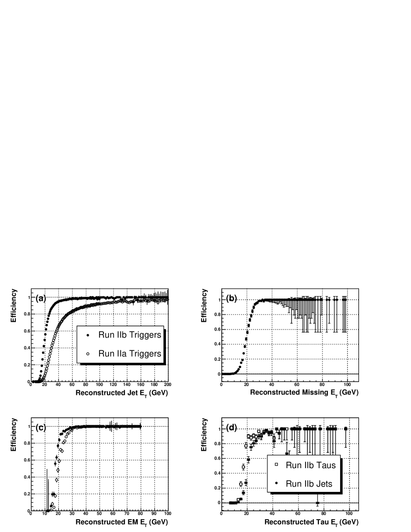
L1Cal algorithm performance has been measured relative to unbiased offline reconstruction of jets, electrons, taus, and missing using runs taken at luminosities greater than 11032 cm-2s-1, with a special “low threshold” trigger list designed to minimize trigger bias in the data. Some of these results are summarized in Fig. 20. In Fig. 20(a), turn-on curves (efficiency vs. reconstructed jet ) are shown for single jet triggers using Run IIb (with a jet-object threshold of 15 GeV) and Run IIa (requiring two TTs with 5 GeV) trigger algorithms. The significantly steeper transition between low and high efficiency for the Run IIb algorithm is evident here. The turn-on curve for the Run IIb 20 GeV threshold missing trigger is shown in Fig. 20(b). The performance of this trigger is comparable to, or better than that observed in Run IIa. EM trigger performance is summarized in Fig. 20(c), for a sample of events, collected using unbiased triggers. The plot shows the efficiency vs. reconstructed EM object for the logical OR of two separate trigger terms, representative of trigger combinations used in electron-based analyses at D0. The Run IIb terms used are a single EM trigger term with a threshold of 19 GeV, or an isolated single EM trigger with a threshold of 16 GeV; while for Run IIa, the requirements are a single TT with EM 16.5 GeV or two TTs with 8.25 GeV. Both of these triggers produce rates of 370–380 Hz at a luminosity of 31032 cm-2s-1. However, the Run IIb trigger combination gives a sharper turn-on and allows for a lower effective threshold, yielding a significantly higher efficiency for selecting decays than that achievable using the Run IIa system. Finally, results using the new Run IIb Tau algorithm are summarized in Fig. 20(d). In this plot, trigger turn-on curves are shown for single tau and single jet triggers using a sample of candidates, selected offline from events collected using unbiased (muon) triggers. The L1Cal tau algorithm allows lower object thresholds to be used (15 GeV taus compared to 20 GeV jets) yielding higher signal selection efficiencies for the same trigger rate.
Measured trigger rates using the new algorithms and trigger list are consistent with those based on extrapolations of Run IIa data to Run IIb instantaneous luminosities, shown in Fig. 8. As can be seen, the total trigger rate observed using the new Run IIb list, to which L1Cal contributes more than 50% of the events, fits into the bandwidth limitations of the experiment. A Run IIa trigger list, designed to give the same selection efficiency as the Run IIb list above, would have exceeded these limits by a factor of two or more.
14 Conclusions
The new D0 Run IIb L1Cal trigger system was designed to cope efficiently with the highest instantaneous luminosities foreseen during the Run IIb operating period of the Tevatron at Fermilab. To accomplish this goal clustering algorithms have been developed using a novel hardware architecture that uses bit-serial data transmission and arithmetic to produce a compact, cost-effective system built using commercially available FPGAs. Although data transmission rates in the system approach one tera-bit per second, the system has been remarkably stable since it began to operate at the beginning of Run IIb.
With the Tevatron regularly producing instantaneous luminosities in excess of 21032 cm-2s-1, the new trigger system has been tested extensively at its design limits. So far it has performed exceptionally well, achieving background rejection factors sufficient to fit within the bandwidth limitations of the experiment while retaining the same or better efficiencies as observed in Run IIa for interesting physics processes.
15 Acknowledgments
We gratefully acknowledge the guidance of George Ginther, Jon Kotcher, Vivian O’Dell, and Paul Padley as managers of the Run IIb project, as well as the technical advice of Dean Schamberger. We would also like to thank Samuel Calvet, Kayle DeVaughan, Ken Herner, Marc Hohlfeld, Bertrand Martin, and Thomas Millet for analyzing L1Cal data and for producing the performance plots shown in this paper. Finally, we thank the staffs at Fermilab and the collaborating institutions, and acknowledge support from the DOE and NSF (USA); CEA (France); and the CRC Program, CFI and NSERC (Canada).
References
-
[1]
Tevatron Run II Handbook.
http://www-bd.fnal.gov/lug/ - [2] V.M. Abazov, et al., Nucl. Instrum. and Methods A 565, 463 (2006).
-
[3]
The Tevatron Run II Upgrade Project.
http://www-bd.fnal.gov/run2upgrade/ - [4] R. Lipton, Nucl. Instrum. and Methods A 566, 104 (2006); M. Weber, Nucl. Instrum. and Methods A 566, 182 (2006).
- [5] M. Abolins, et al., IEEE Trans. on Nucl. Sci. 51, 340 (2004).
- [6] S. Abachi, et al., Nucl. Instrum. and Methods A 338, 185 (1994).
- [7] The right-handed D0 coordinate system is defined with the -axis in the direction of the proton beam, with measuring the azimuthal angle in the plane transverse to the beam direction, with measuring the polar angle, and with the pseudo-rapidity, .
- [8] M. Abolins, D. Edmunds, P. Laurens and B. Pi , Nucl. Instrum. and Methods A 289, 543 (1990).
-
[9]
See for example:
The ATLAS Level-1 Trigger Group, ATLAS Level-1 Trigger Technical Design Report, http://atlas.web.cern.ch/Atlas/GROUPS/DAQTRIG/TDR/tdr.html ATLAS TDR-12 (1998).
The CMS Collaboration, The TriDAS Project Technical Design Report,
Vol. 1: The Trigger Systems,
http://cmsdoc.cern.ch/cms/TDR/TRIGGER-public/trigger.html, CERN/LHCC 2000-38 (2000).
J. Alitti, et al., Z. Phys. C49, 17 (1991). - [10] The D0 collaboration, Run IIb Upgrade Technical Design Report, Fermilab-Pub-02/327-E (2002).
-
[11]
WIENER, Plein & Bauss Ltd.
http://www.wiener-us.com/ -
[12]
3M Corporation, Pleated foil shielded cable (90211 Series)
http://www.3m.com -
[13]
Analog Devices, 10-Bit 40 MSPS 3 V Dual A/D Converter (AD9218BST-40)
http://www.analog.com -
[14]
Xilinx, Virtex-II FPGA (XC2V1000-4FG456C)
http://www.xilinx.com/ -
[15]
National Semiconductor, 48-bit Channel Link SER/DES (DS90CR483/4)
http://www.national.com -
[16]
W. L. Gore & Associates, Inc., Eye-Opener Millipacs 2 / Z-Pack 2mm HM
Cable Connector (2MMS02xx)
http://www.gore.com -
[17]
Altera, Stratix Device Family (EP1Sxx)
http://www.altera.com
(EP1S20F780C7, EP1S20F780C6, EP1S10F780C6, and EP1S30F1020C6 devices are used for the TAB SWA, TAB global, GAB LVDS and GAB S30 FPGAs, respectively.) -
[18]
Agilent Technologies, Transmit/Receive Chip
Set (HDMP-1022)
http://www.agilent.com
Stratos Optical Technologies, Optical Gbit Dual Transmitter (M2T-25-4-1-L)
http://www.stratoslightwave.com -
[19]
Altera, Cyclone Device Family (EP1C6Q240C7)
http://www.altera.com -
[20]
Altera, Serial Configuration Device (EPCS4SI8)
http://www.altera.com -
[21]
Cypress Semiconductor Corporation, Clock Distribution Buffer (CY29948AI)
http://www.cypress.com -
[22]
Fairchild Semiconductor, TTL to ECL Converter (FDLL4148)
http://www.fairchildsemi.com - [23] National Semiconductor, Differential Line Drivers/Receivers (DS90LV047/8 ATMTC) http://www.national.com
- [24] As currently implemented the North, Central and South regions correspond to , , and , respectively.
-
[25]
Altera, ACEX 1K Series FPGA (EP1K50QC208-2)
http://www.altera.com - [26] Because of the extra latency involved in the divide operation necessary for the calculation of the Tau algorithm isolation, this information is not available in time for transmission to the L1CalTrk system.
-
[27]
GE Fanuc Embedded Systems, PCI to VME bus adapter (Model 618)
http://www.gefanucembedded.com -
[28]
Vertical Interface Board Documentation.
http://www-linac.fnal.gov/LINAC/hardware/vmesys/boards/vi/ viInfo.html -
[29]
Python Programming Language – Official Website.
http://www.python.org -
[30]
TkInter Documentation Website.
http://wiki.python.org/moin/TkInter -
[31]
W3C: Extensible Markup Language Website.
http://www.w3.org/XML/ -
[32]
The ADAPTIVE Communication Environment Website.
http://www.cs.wustl.edu/schmidt/ACE.html -
[33]
R. Brun, et al.,
ROOT: An Object-Oriented Data Analysis Framework.
http://root.cern.ch/root/