Ab initio study of misfit dislocations at the SiC/Si(001) interface
Abstract
The high lattice mismatched SiC/Si(001) interface was investigated by means of combined classical and ab initio molecular dynamics. Among the several configurations analyzed, a dislocation network pinned at the interface was found to be the most efficient mechanism for strain relief. A detailed description of the dislocation core, and the related electronic properties, are discussed for the most stable geometry: we found interface states localized in the gap that may be source of failure of electronic devices.
pacs:
68.35.-p, 81.05.Hd, 81.15.AaIn recent years the development of several sophisticated epitaxial growth techniques has allowed to produce new interesting materials and heterostructures, even in the presence of high lattice mismatch between the constituent phases. Furthermore, high-resolution electron microscopy (HREM) and other similar techniques deepened the characterization of such systems, providing a description of the interface quality and epitaxial relations of the sublattices. Nevertheless, the atomic structure and the chemical environment at the interface, which deeply affect its physical properties, still remain hardly accessible to any experimental technique.
Atomistic simulations represent a powerful tool to complement the experimental data. Though recent theoretical works appeared on the study of lattice mismatched interfaces for some specific system involving ceramic materials benedek , the ab initio study of a mismatched semiconductor/semiconductor interface, where the complex covalent bonding requires an accurate description of charge transfer ref14 , is far to be complete inas . Among all the possible high misfit heterostructures, we focussed on the (001) interface between cubic silicon carbide (-SiC) and silicon (Si) without lacking of generality. This system, characterized by a peculiar 20 difference in lattice parameters between the two constituents, can be considered as a template of high lattice mismatched heterojunctions, where an ab initio approach is still affordable. Furthermore, it is technologically interesting, because of the outstanding physical properties of -SiC, a possible candidate for applications in harsh environment devices capano . Some recent results on the study of this heterostructure exp evidenced that the interface can be prepared so to be locally abrupt, with a network of pure edge misfit dislocations localized at the interface to accommodate the extreme lattice mismatch. The formation of a dislocation network as an efficient mechanism of strain release usually occurs in heterostructures with a mismatch larger than 10 trampert .
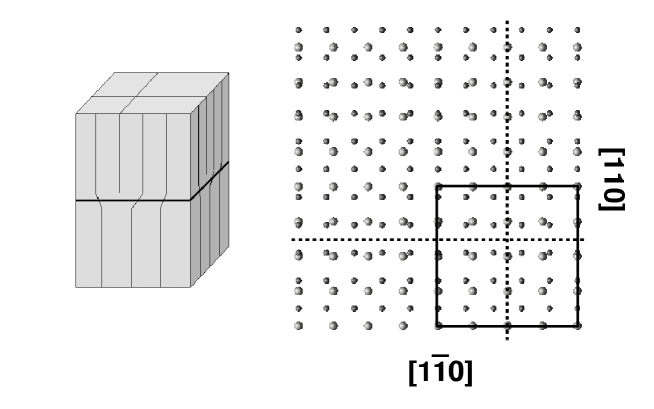
The occurrence of edge dislocations can be treated in the frame of the well established near coincidence lattice model epi , which asserts that the lowest interfacial energy configurations are obtained when a perfect coincidence site between two dissimilar structures is realized. Given two materials with lattice parameters and , a perfect coincidence site occurs when =m/n, with m and n positive integers. For the -SiC/Si(001) system, m=5 and n=4 respectively: since m=n+1, only one extra lattice plane is needed along each of the two primitive directions of the coincidence lattice cell to release almost all the misfit strain, in agreement with HREM images exp ; oldapl . A network of misfit dislocations will thus be generated in the SiC film starting at the interface.
In order to characterize the heterostructure and provide an accurate description of its structural and electronic properties, we performed a combined classical and ab initio molecular dynamics study of different dislocation core structures: the minimum energy system, i.e. the most efficient way for strain release, is obtained for dislocations pinned at the SiC/Si interface, originating at a sub-stoichiometric, C terminated layer.
To reproduce the experimental situation, we considered a periodically repeated multilayer: the interface was built by matching a p(4x4)-Si(001) with a p(5x5)-SiC(001) slab, at the Si lattice parameter optimized for bulk calculations with the chosen potentials (either classical or ab-initio). This model contains two edge dislocations in the supercell, one along each of the two directions perpendicular to the interface, and the periodicity experimentally observed is thus respected. In Fig. 1 the interface structure is schematically represented and the coincidence lattice supercell, which we considered in our calculations, is evidenced. At the interface, the dislocation directions are not equivalent, because of the zincblende stacking: this renders inequivalent the dislocation cores.
We have performed a structural optimization for several possible interface configurations, varying both geometry and stoichiometry, via classical and ab initio Molecular Dynamics (MD) methods in order to get the most stable structure. The relative energy of systems containing different numbers of atoms has been discussed in the grand canonical scheme chempot .
Classical MD for several interface configurations allowed us to select the core dislocation structures and slab size for the ab initio simulations. The Si-Si, Si-C and C-C interactions were modelled by means of the empirical Tersoff’s potentials tersoff2 . It has recently been demonstrated that these potentials give formation energies and properties of native defects in -SiC(001) in good agreement with ab initio calculations nuclear . We performed tests varying the stoichiometry at the interface and the core dislocation distance from the interface. In order to prevent the interaction between the interface and the slab surfaces, we considered thick slabs (36 SiC layers on top of 36 Si layers: in the following, we will indicate the systems as N/M, where N (M) stems for the number of SiC (Si) layers, thus the slab described above will be labelled as 36/36). All the atoms were allowed to move, except those belonging to the outermost layers, which were constrained to relax in a collective way. Our results indicate that configurations with C atoms at the interface are always more stable. A pseudomorphic SiC layer on top of Si, before the dislocations start, is unfavorable. In agreement with experimental results exp , the favored core structures are those with the dislocations pinned at the interface nota . Among all the considered geometries, we focussed on the most meaningful ones: the stoichiometric interface and the one which is lowest in energy. The latter is obtained from the stoichiometric solution by removal of all the C atoms along the two core dislocation lines (13 atoms per supercell): this configuration gives an energy gain E of 1.12 J/m2 (16.43 eV/cell-area) and 0.48 J/m2 (7.07 eV/cell-area) for C-poor and C-rich conditions respectively chempot , in classical MD and for a 36/36 slab.
In order to determine the minimum size required to get accurate results via ab initio techniques, we analyzed how the relative energies and atomic structures of these two systems vary as a function of the slab thickness, in classical MD calculations. We observed that the relative atomic distortion is less than 2 after the 4th layer, when considering a 5/5 or a 36/36 layer slab; furthermore, the value obtained for E for the two configurations described above in a 7/7 slab reproduces correctly the asymptotic value of an infinite (36/36) system. When a 5/5 slab is considered, E decreases by in C-poor conditions (i.e. E = 12.75 eV/cell-area), due to a stronger surface-interface interaction obtained in the non-stoichiometric structure. These results, that provide a good estimate for the system stability, allowed us to consider only the 5/5 slab in ab initio calculations.
The ab initio MD hamann simulations were performed in the frame of density functional theory (DFT), in the local density approximation (LDA) LDA . The electronic wavefunctions (charge density) were expanded in plane waves with an energy cutoff of 40 (160) Ry; only the point was included for the integration in the supercell Brillouin Zone (BZ). The electron-ion interaction was described by fully non local pseudopotentials hamann . Surface atoms at both sides were saturated with hydrogen, at a distance optimized via preliminary surface calculations nota1 . All the atoms of the slab were allowed to move except the hydrogens and the Si (C) in the outermost layers, which were relaxed along the direction perpendicular to the surface only. In a subsequent test, this constrain has been released in order to evaluate the interaction between surfaces and interfaces. Structures were considered converged when forces acting on atoms were less than 10-4 a.u. (0.005 eV/Å) and energy varied by 10-5 eV/atom.
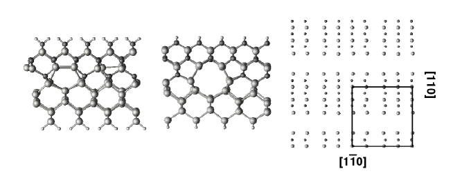
We observed that the classical simulations give good initial guess geometries for ab initio calculations, though lacking of accuracy in predicting structures where dangling bonds are present. In particular, at variance with the empirical simulation, the stoichiometric system reconstructs around the two dislocation cores, where dangling bonds are localized, if relaxed by the ab initio technique. The core structures are thus characterized by 5- and 7-membered rings with C-C and Si-Si dimers at the SiC and Si interface layers respectively nota2 . The same energy ordering was however found in the two different methods: the sub-stoichiometric solution is the most stable in the full physical range of variability of the C chemical potential. The ab initio energy gain for this geometry is E = 14.9 (5.6) eV/cell-area, in C-poor (C-rich) conditions.
The relaxed structure for the lowest energy interface is reported in Fig. 2. The interplanar distance at the interface is lower (-13) than the one obtained in bulk SiC: the deformation optimizes the SiC cell volume and bond distances at this high lattice mismatch. We observed that both Si-Si (in Si) and Si-C bonds (in SiC and at the SiC/Si interface) are stretched at the dislocation cores, compared to the bulk bond lengths, being elongated up to 2.5 Å and 2.0 Å, respectively. The tetrahedral configuration is distorted too, with some Si-C-Si bond angles close to 120∘. The bulk structure is quickly recovered when moving away from the interface and at the third atomic layer the residual distortions are already small (3 in bond distances, interplanar spacing and angles). The deformation induced by the interface and the dislocation cores has been also analyzed in terms of warping of the atomic layers (see right panel in Fig. 2). We found that the major deformations are localized in Si, since it has smaller elastic constants than SiC. The layer puckering decreases when moving aside the interface: this is in nice agreement with some recent experimental results warp on the structural characterization of SiC films grown on a Si(001) substrate, which evidenced an internal roughness of individual SiC planes fading away from the Si substrate. As noticed in Fig. 2, the sub-stoichiometric structure does not present any dangling bond: the Si atoms in the second SiC layer, which would have an unsaturated bond, reconstruct and form dimers 2.4-2.5 Å long; this is also evidenced by the analysis of the electronic structure (see below) which proves the presence of bonding charge density localized between interfacial Si atoms. The removal of C atoms and stretched C dimers in the core allows to better accommodate the misfit strain, although maintaining an abrupt SiC/Si interface: this stabilizes the system with respect to the stoichiometric one.
In order to have a qualitative indication of the interface/surface interaction, we performed further calculations on the 5/5 slab, relaxing the surface atoms at both sides. The results of these simulations indicate that already for the 5/5 system the interface is well described, and the interaction with the surface is small: the bond lengths around the dislocation cores change less than 3 and the energy difference between the stoichiometric and sub-stoichiometric slabs is modified by 18 for C-poor conditions. The major distortions obviously occurs at surface layers, that bent to accommodate the residual elastic strain (z = 0.9Å).
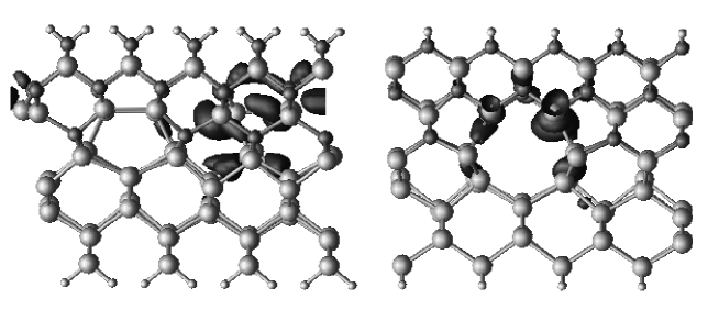
The interface structure determines the electronic properties of the heterojunction. In particular, the presence of defects such as misfit dislocations can induce interface states, also called interface trapped charges, localized in the band gap, that may be responsible for device failure. We have analyzed the electronic structure for the most stable dislocation network at the -SiC/Si(001) interface. Although the number of dangling bonds is minimized in this system, the Highest Occupied (HO) and Lowest Unoccupied (LU) states are localized in the core of the edge dislocations, as a result of the large difference in charge transfer between Si-C and Si-Si bonds. These states lay in the interface band-gap, at 0.8 and 1.3 eV above the valence band top at nota3 , thus they may be a perturbation to the electron mobility and optical properties of the SiC/Si heterostructure. In Fig. 3, the charge density plot of the HO state along the two dislocation directions is represented. The charge density is mainly localized on atoms of the [10] core dislocation, while no density is observed around the core in the perpendicular direction. The opposite situation is found in other bonding states localized in the system forbidden gap and for the LU state (not shown) which charge densities pertain to the dislocation core existing along the [110] direction.
In conclusions, using classical and first-principles calculations, we have presented a comparative analysis of the structural and electronic properties of edge dislocation networks at a high lattice mismatched semiconductor/semiconductor interface. For the studied case, -SiC/Si(001), the core dislocations which were found as most stable, and which are thus responsible for strain relief in the heterostructure, are pinned at the interface, and occur at sub-stoichiometric C layers. The presence of these extended defects is responsible for occupied and unoccupied states, laying in the forbidden gap, which can severely affect the electronic properties of the system.
One of us (LP) acknowledges INFM support for his stay in Italy as visiting professor. GC acknowledges Demichelis Foundation for his PhD fellowship. We also wish to thank Alexis Baratoff for fruitful discussions. Calculations performed in CINECA (IT) through the INFM Parallel Computing Initiative and at CSCS (Manno, CH). This work was partially supported by INFM-PRA:1MESS.
References
- (1) R. Benedek, et al., Phys. Rev. Lett. 84, 3362 (2000); R. Benedek, et al., Phys. Rev. B 60, 16094 (1999).
- (2) G. Galli, F. Gygi, and A. Catellani, Phys. Rev. Lett. 82, 3476 (1999).
- (3) N. Oyama, et al., Surf. Sci. 433-435, 900 (1999).
- (4) See, e.g., M. A. Capano, and R. J. Trew, Mater. Res. Bull. 22, 19 (1997).
- (5) C. Long, S. A. Ustin, and W. Ho, J. Appl. Phys. 86, 2509 (1999).
- (6) S. R. Nutt, et al., Appl. Phys. Lett. 50, 203 (1987).
- (7) A. Trampert, and K. H. Ploog, Cryst. Res. Technol. 35, 793 (2000).
- (8) N. H. Fletcher, and K. W. Lodge, Epitaxial Growth, Part B, in J. W. Matthews (ed.), Academic Press, New York, 529 (1975).
- (9) G. X. Qian, R. M. Martin and D. J. Chadi, Phys. Rev. B 38, 7649 (1988). We varied the chemical potential between the total energy of bulk Si (as obtained consistently) and that of bulk Si minus the heat of formation of the SiC crystal (the experimental value is Hf = 0.72 eV). The equation = + holds in the full physical range: this defines C-poor and C-rich conditions respectively as the two extrema mentioned above.
- (10) J. Tersoff, Phys. Rev. B 39, 5566 (1989).
- (11) F. Gao, et al., Nucl. Instr. and Meth. B 180, 286 (2001).
- (12) This corresponds to a vanishing critical thickness for SiC overlayers on Si.
- (13) We used the first principles molecular dynamics programs BASIC96 and JEEP (G. Galli and F. Gygi). For a review see, e.g., G. Galli and A. Pasquarello, in Computer Simulation in Chemical Physics, Edited by M.P.Allen and D.J.Tildesley, p. 261, Kluwer, Dordrecht (1993); and M. C. Payne, et al., Rev. Mod. Phys. 64, 1045 (1993). Pseudopotentials generated as in D.R. Hamann, Phys. Rev. B 40, 2980 (1989). (We used s and p nonlocality for Si and s nonlocality for C).
- (14) W. Kohn, and L. Sham, Phys. Rev. A 140, 1133 (1965).
- (15) These tests were performed with symmetric slabs of 13 layers, plus a H terminating overlayer at both surfaces. In this case, a surface periodicity was considered (4 atoms/layer) and all the atoms were allowed to move.
- (16) A full description of the energetics, the structural and electronic properties of the investigated systems, along with a detailed analysis of the strain field within elasticity theory will be presented in a forthcoming publication.
- (17) G. Xu, and Z. C. Feng, Phys. Rev. Lett. 84, 1926 (2000).
- (18) The valence band widths of Si- and SiC-derived bulk states compare fairly well for relaxed and unrelaxed surfaces, although underestimate the respective bulk calculations. Furthermore they change by when increasing the slab thickness to 7/7. We were thus able to estimate an error of 0.2 eV on LDA eigenvalues. The energy positions of HO and LU states, with respect to the valence band top of the bulk constituents, as obtained in this work, are beyond these limits.