Auger recombination and carrier multiplication in embedded silicon and germanium nanocrystals
Abstract
For Si and Ge nanocrystals (NCs) embedded in wide band-gap matrices, Auger recombination (AR) and carrier multiplication (CM) lifetimes are computed exactly in a three-dimensional real space grid using empirical pseudopotential wave functions. Our results in support of recent experimental data offer new predictions. We extract simple Auger constants valid for NCs. We show that both Si and Ge NCs can benefit from photovoltaic efficiency improvement via CM due to the fact that under an optical excitation exceeding twice the band gap energy, the electrons gain lion’s share from the total excess energy and can cause a CM. We predict that CM becomes especially efficient for hot electrons with an excess energy of about 1 eV above the CM threshold.
pacs:
72.20.Jv, 73.22.-fI Introduction
The Group IV semiconductor, Si and to a lesser extend, Ge have been indispensable for the electronics and photovoltaics industry. The recent research efforts have shown that their nanocrystals (NCs) bring new features which fortify their stands. For instance, NCs can turn these indirect band-gap bulk materials into light emitters ossicini or offer increased efficiencies in solar cells. nozik-jap The latter has been demonstrated in a very recent experimental study nozik-nl by significantly increasing the solar cell efficiency in colloidal Si NCs due to carrier multiplication (CM) which enables multiple exciton generation in response to a single absorbed photon. schaller ; ellingson Similarly, the inverse process, Auger recombination (AR) is also operational and it introduces a competing mechanism to CM which can potentially diminish the solar cell efficiency and in the case of light sources it degrades the performance by inflating the nonradiative carrier relaxation rate. klimov-rev
The utilization and full control of both CM and AR require a rigorous theoretical understanding. The pioneering series of theory publications on the AR in Si NCs belong to a single group based on an atomistic tight binding approach. mihalcescu ; delerue1 ; delerue2 Unfortunately, they only considered hydrogen passivated Si NCs without addressing the shape effects. Moreover, their results do not reveal a size-scaling for AR but rather a scattered behavior over a wide band of lifetimes in the range from few picoseconds to few nanoseconds as the NC diameter changes from 2 to 4 nm. In the past decade, no further theoretical assessment of AR in Si NCs was put forward. In this context, the Ge NCs have not received any attention although with their narrower effective band gap, they can benefit more from the low-energy part of the solar spectrum in conjunction with CM for increasing the efficiency.
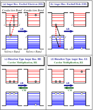
In this work we provide a theoretical account of AR and CM in Si and Ge NCs which reveals their size, shape and energy dependence. Another important feature of this work, unlike commonly studied hydrogen-passivated NCs is that we consider NCs embedded in a wide band-gap matrix which is essential for the solid-state device realizations. Similar to the classification of Wang et al. in their theoretical work on Coulombic excitations in CdSe NCs, wang03 we consider different possibilities of AR as shown in Fig. 1. We use the type of the exicted carrier as the discriminating label, hence we have the excited electron (Fig. 1(a)) and the excited hole (Fig. 1(b)) AR and their biexciton variants (Fig. 1(c) and (d)). All of these have corresponding CM processes taking place in the reverse direction but only the CM in Fig. 1(c) and (d) are studied as they can be optically induced.
II Theoretical Details
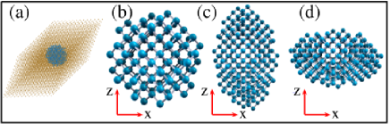
Both AR and CM require an accurate electronic structure over a wide energy band extending up to at least 3-4 eV below (above) the highest occupied molecular orbital-HOMO (lowest unoccupied molecular orbital-LUMO). Another constraint is to incorporate several thousands of core and host matrix atoms within a supercell (see Fig. 2 (a)). To meet these requirements we have employed the linear combination of bulk bands basis within the empirical pseudopotential framework which can handle thousands-of-atom systems both with sufficient accuracy and efficiency over a large energy window. wang97 Details regarding its performance and the implementation such as the wide band-gap host matrix can be found in Ref. bulutay07, . We should mention that Califano et al. have successfully employed a very similar theoretical approach in order to explain the hole relaxation in CdSe NCs. califano
After solving the atomistic empirical pseudopotential Hamiltonian for the energy levels and the wave functions, the AR and CM probability can be extracted using the Fermi’s golden rule,
| (1) |
where and are respective initial and final configurations with the corresponding energies and , respectively, and is the level broadening parameter which is taken as 10 meV. However sensitivity to this parameter is also considered in this work. The spin-conserving screened Coulomb potential is given by . The subject of screened Coulomb interaction in NCs is an active source of debate; recent publications predict reduced screening ogut03 ; trani06 whereas, other theoretical investigations allan ; wang03 have concluded that the inverse dielectric function is bulklike inside the NC. Therefore, we follow wang03 and use
| (2) |
as the inverse dielectric function, where, the so-called mask function is set to 1 when inside of the NC and 0 when outside of the NC.
Expressing the initial and final states of the AR shown in Fig. 1 (a) or (b) by using the Slater determinant, the matrix elements () can be calculated as
| (3) | |||||
here the labels , and and refer respectively to the initial and final states which also include the spin and is volume of the supercell.
These matrix elements, are computed exactly in a three-dimensional real space grid without resorting to any envelope approximation. The number of final states are determined setting the final state window to around the exact conserved energy . For the initial states and , Boltzmann average is taken into account due to thermal excitations. The same should apply to the other initial state , however, as a safe but computationally very rewarding simplification it is kept fixed at LUMO for the excited electron (EE), and at HOMO for the excited hole (EH) type AR.
III Results and Discussions
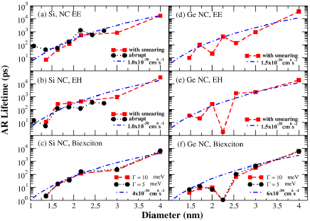
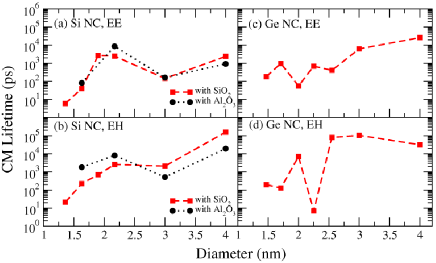
We first apply this formalism to spherical NCs (see Fig. 2(b)) having abrupt interfaces. The corresponding AR lifetimes for EE and EH processes are plotted as a function of NC diameter in Fig. 3 (a) and (b). The point symmetry of the NCs in the case of abrupt interface between NC core and the matrix causes oscillations in the physical quantities such as the state splittings and the density of states with respect to NC diameter. bulutay07 When we account for the interface transition region between the NC and host matrix, daldosso we observe that these strong oscillations in the size dependence of AR are highly reduced for Si and Ge NCs (cf. Fig. 3). The interface region especially affects the excited state wave functions and the final state density of states and it makes our model more realistic for both Si and Ge NCs. As an observation of practical importance, we can reproduce our data remarkably well (cf. Fig. 3) using the simple expression , with an Auger coefficient of cm6s-1 for Si NCs and cm6s-1 for Ge NCs, where is the carrier density within the NC such that there should be two electrons or holes to initiate an AR.
The other two types of AR shown in Fig. 3 (c) and (f) refer to biexciton recombinations. This process becomes particularly important under high carrier densities such as in NC lasers or in solar cells under concentrated sunlight. Its probability can be expressed in terms of EE and EH type AR as, wang03 where and are EE and EH lifetimes. Fig. 3 (c) and (f) compares the computed biexciton type AR for Si and Ge NCs with the expression where the value cm6s-1 and cm6s-1 are used which are obtained from the previous values extracted for EE and EH processes together with the expression. For Si NC case, our calculated value at 3 nm diameter agrees reasonably well with the experimental photoluminescense decay time of about 105 ps which was attributed to AR. troje In Fig. 3 (c) and (f), we also demonstrate the fact that a choice of meV does not introduce any marked deviation from the case of meV as used in this work for both Si and Ge NCs. This parameter test automatically checks the sensitivity to the final state energy window chosen as 7.
| Spherical | Prolate | Oblate | ||||
|---|---|---|---|---|---|---|
| (nm) | 1.63 | 2.16 | 1.63 | 2.16 | 1.63 | 2.16 |
| EE (ps) | 40 | 541 | 32 | 103 | 36 | 121 |
| EH (ps) | 267 | 430 | 74 | 76 | 26 | 139 |
Next, we demonstrate the effects of deviation from sphericity on Si NCs. We consider both oblate (Fig. 2(c)) and prolate (Fig. 2(d)) ellipsoidal Si NCs described by the ellipticity value of =0.85. For the comparison purposes, we preserve the same number of atoms used in spherical NCs of diameters 1.63 and 2.16 nm. The results listed in Table 1 indicate that the spherical NC has a lower Auger rate than the aspherical shapes. This can be reconciled as follows: in the case of either prolate or oblate NC, the electronic structure is modified in such a way that the number of final states is increased, furthermore, a coalescence of the states around the HOMO and LUMO occurs. A similar effect was also observed in the asphericity-induced enhancement of Auger thermalization of holes in CdSe NCs. califano However, we should note that the shape effects are not pronounced.
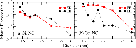
In their work on the CM in PbSe NCs, Allan and Delerue have deduced that such Coulombic interactions are primarily governed by the state-density function. allan06 Even though we agree on the importance of the density of states, we would like to emphasize the significant role of the Coulomb matrix elements. We illustrate our point by Fig. 4, where the average matrix element for Si and Ge NCs are shown. The strong size dependence leading to a variation over several orders of magnitude indicates their nontrivial role.
Regarding the CM, we first consider the inverse Auger process (cf., Fig. 1 (c) and (d)) for different diameters of the Si and Ge NCs. Therefore, we consider the impacting electron (hole) to have an energy of above (below) the conduction (valence) band edge i.e., just at the threshold energy to initiate a CM event. As seen in Fig. 5, EE and EH type CM lifetimes for Si and Ge NCs decrease from the few ns to few ps as the NC diameter decreases. However, for EE (EH) type CM, the small number of final states at the bottom of the CB (top of the VB) cause a nonmonotonic dependence of CM on size of the NC.
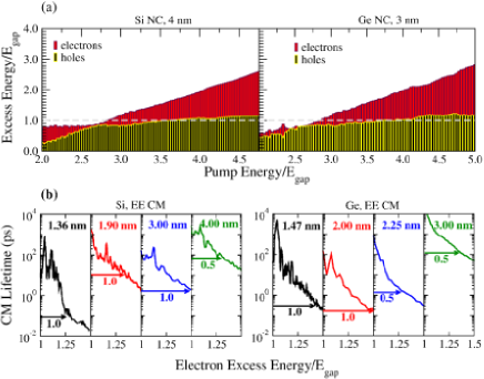
From the practical point of view, the investigation of the effect of excess energy on the CM under an optical excitation above the effective gap, is even more important. Here, the correct placement of excited electron and hole after optical excitation is critical. We assign the excited electron and hole to their final states by accounting for all interband transitions with the given energy difference as weighted by the dipole oscillator strength of each transition which is a direct measure of the probability of that particular event. In Fig. 6 (a) we observe that the electrons receive the lion’s share of the total excess energy which is the desired case for the high efficiency utilization of CM in photovoltaic applications. werner Our threshold value of 2.8 for Si NCs is somewhat higher than the recent experimental data. nozik-nl In Fig. 6 (b) we show the corresponding electron-initiated CM lifetimes as a function of excess energy. It can be observed that CM is enhanced by more than two orders of magnitude within an excess energy of 1 eV beyond the CM threshold reaching a lifetime of few picoseconds.
IV Conclusions
To summarize, we offer a theoretical assessment of the two most important Coulombic excitations, AR and CM, in Si and Ge NCs. The Auger coefficients that we extracted can serve for the practical needs in the utilization of this process. For the efficiency enhancement via CM in Si and Ge NCs, the prospects look positive as the hot electrons receive most of the excess energy and they can undergo a CM within few picoseconds.
Acknowledgements.
This work has been supported by the European FP6 Project SEMINANO with the Contract No. NMP4 CT2004 505285 and by the Turkish Scientific and Technical Council TÜBİTAK with the Project No. 106T048. The computational resources are supplied in part by TÜBİTAK through TR-Grid e-Infrastructure Project.References
- (1) S. Ossicini, L. Pavesi, and F. Priolo, Light Emitting Silicon for Microphotonics, Springer-Verlag, Berlin, (2004).
- (2) M. C. Hanna and A. J. Nozik, J. Appl. Phys. 100, 074510 (2006).
- (3) M. C. Beard, K. P. Knutsen, P. Yu, J. M. Luther, Q. Song,W. K. Metzger, R. J. Ellingson, and A. J. Nozik, Nano Lett. 7, 2506 (2007).
- (4) R. D. Schaller and V. I. Klimov, Phys. Rev. Lett. 92, 186601 (2004).
- (5) R. J. Ellingson, M. C. Beard, J. C. Johnson, P. Yu, O. I. Micic, A. J. Nozik, A. Shabaev, A. L. Efros, Nano Lett. 5, 865 (2005).
- (6) V. I. Klimov, J. Phys. Chem. B 110, 16827 (2006).
- (7) I. Mihalcescu, J. C. Vial, A. Bsiesy, F. Muller, R. Romestain, E. Martin, C. Delerue, M. Lannoo, and G. Allan, Phys. Rev. B 51, 17605 (1995).
- (8) C. Delerue, M. Lannoo, G. Allan, E. Martin, I. Mihalcescu, J. C. Vial, R. Romestain, F. Muller and A. Bsiesy, Phys. Rev. Lett. 75, 2228 (1995).
- (9) M. Lannoo, C. Delerue, and G. Allan, J. Lumin. 70, 170 (1996).
- (10) L. W. Wang, M. Califano, A. Zunger, and A. Franceschetti, Phys. Rev. Lett. 91, 056404 (2003).
- (11) L. W. Wang, A. Franceschetti, A. Zunger, Phys. Rev. Lett. 78, 2819 (1997).
- (12) C. Bulutay, Phys. Rev. B 76, 205321 (2007).
- (13) M. Califano, G. Bester, and A. Zunger, Nano Lett. 3, 1197 (2003).
- (14) S. Öğüt, R. Burdick, Y. Saad, and J. R. Chelikowsky, Phys. Rev. Lett. 90, 127401 (2006).
- (15) F. Trani, D. Ninno, G. Cantele, G. Iadonisi, K. Hameeuw, E. Degoli and S. Ossicini, Phys. Rev. B 73, 245430 (2006).
- (16) G. Allan, C. Delerue, M. Lannoo, and E. Martin, Phys. Rev. B 52, 11982 (1995).
- (17) N. Daldosso, M. Luppi, S. Ossicini, E. Degoli, R. Magri, G. Dalba, P. Fornasini, R. Grisenti, F. Rocca, L. Pavesi, S. Boninelli, F. Priolo, C. Spinella, and F. Iacona, Phys. Rev. B 68, 085327 (2003).
- (18) F. Trojánek, K. Neudert, M. Bittner, and P. Malý, Phys. Rev. B, 72, 75365 (2005).
- (19) G. Allan and C. Delerue, Phys. Rev. B 73, 205423 (2006).
- (20) J. H. Werner, S. Kolodinski, and H. J. Queisser, Phys. Rev. Lett. 72, 3851 (1994).