Ti-rich and Cu-poor grain-boundary layers of CaCu3Ti4O12 detected by x-ray photoelectron spectroscopy
Abstract
Cleaved and polished surfaces of CaCu3Ti4O12 ceramics have been investigated by x-ray photoelectron spectroscopy (XPS) and energy dispersive x-ray spectroscopy (EDX), respectively. While EDX technique shows the identical CaCu3Ti4O12 stoichiometry for the two surfaces, XPS indicates that the cleaved surface with grain-boundary layers is remarkably Ti-rich and Cu-poor. The core-level spectrum of Cu 2 unambiguously shows the existence of monovalent copper only for the cleaved surface. Possible grain-boundary structure and its formation are discussed.
pacs:
79.60.-i, 61.72.Mm, 77.84.DyCaCu3Ti4O12 (CCTO) has recently attracted considerable interest due to its extraordinarily high dielectric permittivity () at low frequencies over a wide temperature range (100 K 400 K).Subramanian ; Homes The giant dielectric phenomenon has been primarily elucidated as an extrinsic effect in terms of an internal-barrier-layer-capacitor mechanism. Sinclair It was suggested Sinclair and then confirmed Chung that grain boundary (GB) was the internal barrier for CCTO ceramics. As for CCTO crystals which show even larger dielectric permittivity, Homes internal barriers were still inferred from impedance spectroscopy measurement. Li In fact, CCTO ceramics contains domain boundaries as well as grain boundaries, revealed by scanning electron microscopy and high-resolution transmission electron microscopy. Fang As a result, the detailed dielectric responses of CCTO ceramics can be well interpreted by using a double-barrier-layer-capacitor model. Cao
So far, however, the structure of the internal barriers (grain boundaries and domain boundaries) remains unclear. It was initially suggested that twin boundary was the possible barrier layer. Subramanian A structural model of planar defects due to a twining parallel to planes was recently proposed, Whangbo yet it needs further experimental support. According to a detailed TEM investigation, Wu such twin domains could not be detected in single crystals or polycrystallines, instead, high density of dislocations and cation-disorder-induced planar defects were observed. Very recently, x-ray diffraction under extremely high hydrostatic and uniaxial compression suggested that CCTO ceramics was composed of grains with stiffer shells and softer cores. Ma If so, the GB layers should be different from the grain interiors in structure and composition. However, another recent reportMLi on Mn-doping effect proposed that the grain and GB regions in CCTO ceramics might consist of the same phase but with slightly different compositions.
In this Letter, x-ray photoelectron spectroscopy (XPS) and energy dispersive x-ray spectroscopy (EDX) were employed to detect the possible differences between a polished surface (PS) and a cleaved surface (CS) of CCTO ceramic samples. For a CS, GB layers remain on the surface because of the relatively weak linkage between grains. In the case of a PS, on the other hand, grain interiors are exposed on the surface. Because the detecting depth of XPS is 1 nm in most cases, Tanuma XPS actually reveals the information of ultra-thin surface layers. In comparison, the information depth of EDX is commonly at the micron scale, thus EDX measures the bulk composition. By examining the CS and PS layers with the two techniques, one may obtain the compositional and structural information, especially for the GB layers.
The CCTO ceramic samples were prepared by conventional solid-state reaction using the powdered chemicals of TiO2 (99.99%), CaCO3 (99.99%), and CuO (99.99%). The starting materials were weighed according to the stoichiometric ratio and mixed thoroughly in an agate mortar. The mixed powder was calcined at 1273 K for 12 h in air. This procedure was repeated for three times to ensure that the samples were in single CCTO phase. Then the calcined powder was pressed into a disk (12 mm2 mm) and a rod (12 mm15 mm) respectively. The pressed specimens were finally sintered in air at 1353 K for 24 h followed by furnace-cooling to room temperature. X-ray diffraction identified single phase for the two specimens. Dielectric measurement with an Agilent 4284A precision LCR meter confirmed that the samples showed the property of giant dielectric permittivity as reported elsewhere. Subramanian ; Cao
Prior to the XPS and EDX measurements, the as-prepared CCTO samples were treated to make a PS and a CS, respectively. For the PS sample, the sintered disk was polished by using CeO2 fine powder, followed by removing the remaining CeO2 with a mixture of nitric acid and hydrogen peroxide. Then it was in turn cleaned in distilled water, ethanol, and acetone with a ultrasonic cleaner. The CS sample was obtained simply by cleaving the rod. As soon as the surface was made, the specimen (mounted on a sample holder) was transferred into the ultra-high vacuum system equipped with an x-ray generator (Mg K, 1253.6 eV) and an Omicron EAC2000-125 analyzer. The shift of core-level spectra due to the charging effect was calibrated using the contaminated C peak located at 284.6 eV. Dobler The XPS intensity was calculated based on the areas of the related peaks. After the XPS experiment, the identical samples were also examined by employing a field-emission scanning electron microscope (SEM, SIRION FEI, Netherlands) equipped with a Phoenix (EDAX) x-ray spectrometer. The samples were coated with very thin layer of gold before they were placed into the SEM chamber.
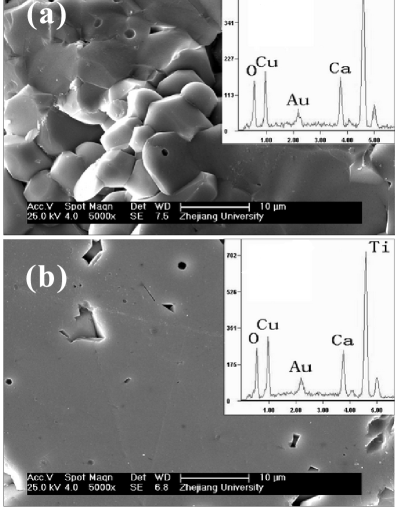
Fig. 1 shows the SEM images of the cleaved and polished surfaces of CCTO ceramics. The CS image shows grain-packed morphology with the grain size of 6 m. One can see that the cleaving takes place mostly at the grain boundaries. For the PS image, a flat surface is shown except for some cavities. This indicates that grain interiors show up due to the polishing. It is also noted that both surfaces have very similar EDX spectra, as shown in the insets of Fig. 1. Quantitative analysis indicates that the atomic ratios (Ca:Cu:Ti) for CS and PS are 1.0:3.1:4.0 and 1.0:3.0:3.8, respectively, consistent with the stoichiometric ratio of CCTO within the experimental errors ( 5%).
Fig. 2 shows the core-level spectra of the cleaved and polished surfaces of CCTO ceramics. Although there is no obvious shift for the positions of the core-level peaks, the relative intensities vary remarkably. As can be seen in the panel (a), the intensities of Ca peaks are similar for the two surfaces. In comparison, the intensity of Cu Auger peak is remarkably weaker for the CS. Accordingly, the intensity of Cu peaks in the panel (b) is also proportionally weaker for the CS. For the Ti peaks in the panel (c), however, the intensity is substantially higher for the CS. In the case of O peak, it is difficult to make a comparison because of the disturbance of surface contamination, especially for the PS sample.

Here we make a quantitative comparing analysis so that the element-specific and instrumental parameters do not need to be concerned. The cation ratio of the PS is assumed to be , because the grain interiors were exposed adequately. Consequently, with the XPS data of the PS as a reference, the composition of the CS was easily determined as (the measurement error, mainly coming from the determination of the peak area, is no more than 5%). Since the information depth is only about 1 nm, the XPS result of the CS reveals the information of the GB layers. Therefore, we conclude that the GB layers are Ti-rich and Cu-poor, compared with the CCTO stoichiometry.
Fig. 3 separately shows the Cu core-level spectra of CCTO ceramics. As can be seen, there is a shoulder at lower energy side of the main peak of only for the CS specimen. By separating the peaks one obtained a small peak at 932.2 eV, suggesting the existence of Cu(I) at GB (similar peak separating for the PS specimen was unsuccessful). Another evidence for the existence of Cu(I) comes from the intensities of the Cu shake-up peaks. The CS sample shows relatively weak shake-up peaks, because Cu(I) has no such component.
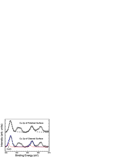
One notes that the amount of excessive Ti is almost equal to the amount of the missing Cu for the CS. This result suggests that some Ti may replace Cu in the GB layers. In fact, evidence of Ti on the Cu site was given in nonstoichiometric Sr0.946(Cu2.946Ti0.054)Ti4O12 Li2 and Na(Cu2.5Ti0.5)Ti4O12. Avdeev In CCTO, however, the Ti on the Cu site is far too small to be detected by refining site occupancies from neutron diffraction data. Li2 Nevertheless, there is a possibility for the GB in which significant amount of Ti occupies the Cu site. The Ti-for-Cu substitution results in monovalent copper due to the charge neutrality, in agreement with the existence of Cu(I) only for the GB layers.
With the clue of Ti on Cu site, Li et al.Li2 proposed an convincing explanation of how CCTO develops conducting regions. At high temperature, Cu(II) reduces to Cu(I) accompanying with a charge compensation via a slight substitution of Ti(IV) on Cu site, forming Ca(CuCuTi)3TiO12. Upon cooling, the Cu(I) converts to Cu(II), liberating electrons into the Ti 3 conduction band. Although this mechanism explains the conductivity of CCTO grains, one could not understand the formation of internal barriers. We notice that the above mechanism ignores the cation migrations during the cooling process. It is possible that the Ti at Cu site migrates to GB layers and domain-boundary layers when cooling down, which forms a Ti-rich and Cu-poor barrier layer.
It is also noted that the structure model proposed by Wu et al. Wu is consistent with the result of Ti-for-Cu substitution in GB layers. The planar defect model involves a lattice shift .Note Such a lattice shift naturally results in cation disorder in Ca/Cu site, accommodating the Ti-for-Cu substitution. The planar defect may give rise to remarkable strain at the boundary, which explains the thermal etching effect within the grains. Fang Furthermore, such a domain-boundary may serves as a stiffer layer as suggested by the high-pressure x-ray diffraction result Ma . Finally, due to the lattice discontinuity, ion-disorder and/or ion displacement, the interface may become a barrier layer against the electron conduction.
In summary, we have revealed the subtle differences in composition of the bulk and grain boundary regions in CCTO ceramics by comparing the core-level spectra of cleaved and polished surfaces. The grain boundary contains remarkably more Ti and less Cu than the grain interior does. Moreover, only the grain boundary layer contains monovalent copper. These results provide crucial insight for the origin of the special giant dielectric phenomenon as well as the grain-boundary structure in CCTO system.
This work was supported by National Science Foundation of China (Grant No. 10274070).
References
- (1) M. A. Subramanian, D. Li, N. Duan, B. A. Reisner, and A. W. Sleight, J. Solid State Chem. 151, 323 (2000).
- (2) C. C. Homes, T. Vogt, S. M. Shapiro, S. Wakimoto, and A. P. Ramirez, Science 293, 673 (2001).
- (3) Derek C. Sinclair, Timothy B. Adams, Finlay D. Morrison, and Anthony R. West, Appl. Phys. Lett. 80, 2153 (2002).
- (4) S. Y. Chung, I. D. Kim, and S. J. L. Kang, Nature Mater. 3, 774 (2004).
- (5) J. Li, A. W. Sleight, and M. A. Subramanian, Solid State Communications 135, 260 (2005).
- (6) T. T. Fang, and C. P. Liu, Chem. Mater. 17, 5167 (2005).
- (7) Guanghan Cao, Lixin Feng, and Cao Wang, J. Phys. D: Appl. Phys. 40, 2899 (2007).
- (8) M.-H.Whangbo and M. A. Subramanian, Chem. Mater. 18, 3257 (2006).
- (9) L. Wu, Y. Zhu, S. Park, S. Shapiro, G. Shirane, and J. Tafto, Phys. Rev. B 71, 014118 (2005).
- (10) Yanzhang Ma, Jianjun Liu, Chunxiao Gao, W. N. Mei, Allen D. White and Jahan Rasty, Appl. Phys. Lett. 88, 191903 (2006).
- (11) Ming Li, Antonio Feteira, Derek C. Sinclair, and Anthony R. West, Appl. Phys. Lett. 88, 232903 (2006).
- (12) S. Tanuma, C.J. Powell and D. R. Penn, Surface and Interface Analysis. 17, 911 (1991).
- (13) D. Dobler, S. Oswald and K. Wetzig, Anal. Bioanal. Chem. 374, 646 (2002).
- (14) J. Li, M. A. Subramanian, H. D. Rosenfeld, C. Y. Jones, B. H. Toby and A. W. Sleight, Chem. Mater. 16, 5223 (2004).
- (15) M. Avdeev and V. B. Nalbandyan, Inorg. Chem. 45, 2217 (2006).
- (16) The original model contains an extra oxygen atom at the interface, what is more, two oxygen atoms are too much close. A more reasonable structure for the planar defect can be simply viewed as shear planes, involving edge-sharing TiO6 octahedra.