Conceptual Design of a Micron-Scale Atomic Clock
Abstract
A theoretical proposal for reducing an entire atomic clock to micron dimensions. A phosphorus or nitrogen atom is introduced into a fullerene cage. This endohedral fullerene is then coated with an insulating shell and a number of them are deposited as a thin layer on a silicon chip. Next to this layer a GMR sensor is fabricated which is close to the endohedral fullerenes. This GMR sensor measures oscillating magnetic fields on the order of micro-gauss from the nuclear spins varying at the frequency of the hyperfine transition (413 MHz frequency). Given the micron scale and simplicity of this system only a few transistors are needed to control the waveforms and to perform digital clocking. This new form of atomic clock exhibits extremely low power (nano watts), high vibration and shock resistance, stability on the order of , and is compatible with MEMS fabrication and chip integration. As GMR sensors continue to improve in sensitivity the stability of this form of atomic clock will increase proportionately.
pacs:
PACSI Background
Atomic clocks have been in existence since 1949. The basic time keeping element is the hyperfine interaction between outer electron(s) and the nuclear spin. Thus embodiments typically use atomic hydrogen, the alkali metals, and ions that have a single outer orbital electron remaining; however hyperfine splitting is present in more general atomic and molecular species and can be used for time keeping. The hyperfine interaction is robust against perturbations from vibration or temperature since it only involves the density and spin of the electron wave function at the nucleus. High quality atomic clocks have time precision of better than 1 part in . Atomic clocks have been reduced to a few cubic millimeters in size. There is a great deal of interest by DARPA and the electronics industry in reducing the size, complexity, and power requirements of atomic clocks. A precise and stable time base that can fit within the packaging and power envelope of modern devices will greatly increase the efficiency and robustness of mobile computing and sensor elements. Spectral bandwidth allocation is fundamentally limited by the accuracy and stability of the reference frequency used to define the clock period. One of the fundamental limits to reducing the size of electronic wireless sensors (motes) is the fact that crystal oscillators cannot be shrunk beyond the current package size[4]. A MEMS-scale atomic clock could replace complex clock synchronization methods within computers and improve arbitration protocols between chips by supplying precise local clocks.
I.1 Atomic Clock Principles
Currently atomic clocks operate by using vapors of Cs or Rb coming off an oven at 80 ∘C. This results in about 1 atom per cubic micron. In some optical clocks buffer gas is used to slow the collision rate of the atoms with the wall where spin flipping occurs – broadening the hyperfine line width. Each atom produces a magnetic field due to the spin of the nucleus – gauss at 1 micron distance. When the atomic system has been excited, the magnetic field oscillates at the hyperfine transition frequency: 100 MHz to 20 GHz – depending upon the atomic species in use. The best current systems use stabilized lasers to interact with the atomic system by means of optical transitions. Thus they do not directly sense the nuclear magnetic field. This method is costly in size and power.
II Endohedral Fullerenes
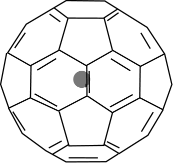
Buckyballs (C60 and C70, each about 1 nanometer in diameter) have been developed that contain a single atomic passenger and even simple molecules[16, 7, 21, 12, 15]. Figure 1 shows a simple model. For most of these endohedral fullerenes a charge transfer of the enclosed atom to the fullerene cage occurs resulting in a chemical bond and distorted structure. In the case of group V atoms the trapped atom is confined by a harmonic-like potential to the center of the cage. The atom is trapped within the covalent bonds of the Buckyball with its outer electrons symmetrically repelled away from the walls of the cage. In almost all respects the atom behaves as a ‘free’ (unbonded) atom, though spatially restricted to be within the fullerene cage. The distributed bonding electrons also act as an almost perfect Faraday cage. The inner atom is fully capable of entering into magnetic interactions since the Buckyball cage is spin neutral (it is desirable to use C12 to remove nuclear spins within the cage walls). Two useful compounds are N@C60 and P@C60, i.e., nitrogen and phosphorus inside C60. Group V atoms are paramagnetic due to their half-filled p-orbitals. Electron Spin Resonance experiments have demonstrated that the trapped electrons for group V atoms have very long spin relaxation times[18].
Group V atoms can be implanted into fullerenes by simultaneous ion bombardment and fullerene evaporation onto a target[18]. The resulting endohedrals are themally[13] and chemically stable[9] at ambient conditions but do show disintegration between 400K and 600K[14]. In low-energy implanted samples only a small fraction are actually filled, typically 1 in 10,000. It is possible to enrich and purify the fraction of filled molecules by high-pressure chromatography[8]. Recent work has shown that nuclear implantation techniques (using 18 MeV ions) can convert almost 6% of a thick fullerene layer (40 m) into endohedral compounds [6]. A Buckyball with an atom trapped within has a nominal diameter of 1 nanometer.
II.1 Endohedral Fullerenes Hyperfine Interactions
Phosphorus comes in one stable isotope: , spin/parity = +. Its electronic ground state, , is split by the hyperfine interaction. Nitrogen comes in two stable isotopes: , spin/parity = 1+ and , spin/parity = -. Both isotopes have their ground state split by the hyperfine interaction. For the sake of concreteness we focus on phosphorous. Nitrogen may require isotopic separation for use in an atomic clock, or, we could accept a double resonance mode of operation.
The contact part of the hyperfine interaction is
| (1) |
where I is the nuclear spin in units of (S is the electon spin). Typical values of the hyperfine frequency are in the microwave range.
One important effect is the increase in electron density at the nucleus due to confinement inside the fullerene. Recent experimental research shows an enhanced electron capture decay rate in when it is encapsulated inside C60[17] .
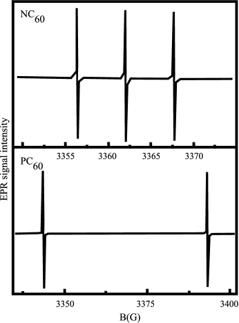
Figure 2 shows EPR experimental data[14] on the P@C60 ground state splitting due to the hyperfine interaction. The doublet splitting (=49.2 G) in the lower panel is due to the hyperfine interaction of the electron spin with the nuclear spin I= of . The EPR spin-magnetic field interaction energy is
| (2) |
This implies a hyperfine frequency of 413 MHz. This is a fairly low hyperfine frequency but reflects that fact that the outer electrons have finite angular momentum, consequently they have zero spatial overlap at the nucleus. The hyperfine interaction in paramagnetic atoms or ions is entirely determined by the admixture of electronic s-orbitals from excited configurations which result from atomic interactions such as electron repulsion and correlation[1].
II.2 Atomic Transitions

Given that P@C60 is a paramagnetic atom the most straightforward method for measuring the hyperfine energy is to polarize the atom in a large static magnetic field. Figure 3 shows the atomic energy levels when the electron spin - magnetic field interaction energy exceeds the hyperfine energy splitting. In the absence of EPR pumping the vast majority of atomic systems will be in the lowest energy state. The polarized outer electron spins will define a spatial direction for the nuclear spin and will define its energy transitions. Usually hyperfine transitions inside paramagnetic atoms and ions have a poorly defined line width – due to the vast number of perturbations acting on the valence electrons, which are directly relayed to the nucleus through the hyperfine interaction. In the case of P@C60 the exceptionally long electron spin relaxation times and the nearly ideal conditions of isolation give us relief from these problems.
II.3 Interactions Between Endohedral Fullerenes
One issue in the use of a packed array of P@C60 molecules for an atomic frequency standard is the perturbation nearby spins apply to each other. Nearby electron spins will contribute varying magnetic energy terms to the nuclear spin. As each nuclear spin will see a slightly different electron spin neighborhood this will broaden the hyperfine frequency of the ensemble. The magnitude of the shift for each electron-nucleus pair is
| (3) |
Table 1 shows this interaction for an electron-nuclear pair as a function of separation.
| Distance [nm] | Frequency Shift |
|---|---|
| 1 | 10 KHz |
| 10 | 10 Hz |
| 100 | 10 mHz |
| 1000 | 10 Hz |
This implies that a close-packed solid of endohedral fullerenes (diameter = 1nm) will exhibit a fractional frequency shift on the order of . In itself this is not a problem as this is a constant shift. The problem stems from the variability of the packing. Randomness in the distances to nearby endohedral fullerenes will modulate the perturbation. This random perturbation will broaden the absorption line of the system resulting in poor short-time frequency control. Assuming stable packing the long term frequency control of the system will still be exemplary.
Since the perturbation term varies as a simple solution could be to dilute the endohedral fullerenes inside a neutral carrier material. The issue now is to estimate the effect of random spacing between endohedral fullerenes and the corresponding perturbation effects so that the net line width of the system meets the short-time frequency requirement. The main problem is the variance in the frequency. Appendix A calculates this effect with the results in Table 2.
| Density of fullerenes [] | [Hz] |
|---|---|
| 5 | |
| 17 | |
| 55 | |
| 172 | |
| 545 | |
| 1,721 | |
| 5,384 | |
| 16,086 | |
| 39,288 | |
| 62,452 |
The conclusion from this calculation is that the divergent interaction amplifies the effect of statistical fluctuations inside a homogenous mixture. While the effects of randomness in fullerene locations limit the ultimate precision of an atomic clock, for less demanding uses, e.g., crystal clock replacement, a simple layer of doped with P by nuclear implantation techniques should prove an attractive option.
A random mixture of endohedral fullerenes is not the best spatial organization for a frequency standard. The best arrangement is a uniform grid with a few 10’s of nm spacing between occupancy sites.
II.4 Glassification of Endohedral Fullerenes
It is possible to separate each endohedral fullerene from its neighbors by coating it with a glass shell. Silica gel, an inorganic polymer, has a three-dimensional network and can easily be synthesized via the sol-gel route. Fullerenes cannot be incorporated into sol-gel glasses homogeneously due to low solubility. This problem can be overcome by functionalization of the fullerenes with such groups as will form some kind of bond (hydrogen, van der Waals, or covalent) with the growing silica network[19]. The synthesis of silica-fullerene hybrid materials is done in the following manner. Silica precursor is mixed with alcohol and water. Acid is added as a catalyst. Functionalized fullerene is added to this mixture directly or by dissolving in toluene. The mixture is allowed to gel over a period of time at elevated temperature. Coatings of single fullerene molecules can be accomplished by performing the above steps in a micro-fluidic mixing chamber where the timed release of materials results in small globules of glass-encased single fullerene.
Fullerene functionalization consists of covalently bonding side groups mainly consisting of nitrogen or Si-O-R (R= Me, Et) or even hydroxyl groups. The molecular carbon allotrope readily adds nucleophiles and carbenes and participates as the electron-deficient dienophile component in many thermal cycloaddition reactions such as the Diels-Alder addition. In all mono-adducts formed by 1,2-addition the fullerene preserves the favorable -electron system of C60[5], however, we can expect a loss of the full symmetry in Buckyball shielding – the net effect on the hyperfine energy of the system needs to be determined by experiment.


So we see that a good arrangement for the endohedral fullerenes is to coat them with 20nm diameter glass coating. This separates the electron-nuclear spins to the point where a narrow line width is possible. It should be noted that wrapping polymers around fullerenes is also a separation option.
Another embodiment which avoids the possible problems of functionalization is to create simple fullerenes and then implant them at low energy into an insulating matrix. We can also use patterning (e.g., 2D interference patterns from hard or soft UV light) to create openings in a photoresist layer. Next we implant a low flux of fullerenes so as to only deposit at most one fullerene per opening. Follow by a thin layer of an insulating material and so on. Finally the photoresist layer with the extra fullerenes is burned off by an oxygen plasma. There are many techniques used in electronics that can create well-separated fullerene matrices.
II.5 Magnetic Parameters for Encapsulated Endohedral Fullerenes
If we assume a uniform sample of 20nm diameter glass spheres with a single fullerene inside we predict an internal magnetic field from the nuclear spins of
| (4) |
At the same time the internal magnetic field from the electron spins is
| (5) |
Because the source of the polarizing field for the nuclear spin is the electron spin coupled through the hyperfine interaction we need to re-express this in terms of the effective magnetic field being applied to the nucleus. Translating the 413 Mhz hyperfine frequency into a nuclear Zeeman splitting gives an equivalent magnetic field of 27 tesla. For the coupling term we have
| (6) |
It should be noted that the interaction energy represented by this pseudo magnetic field is very precisely defined – it is the hyperfine energy. This expression for the interaction will allow us to directly employ the Bloch equations below to predict electron spin precession perturbations on nuclear polarization.
One of the design challenges for the atomic clock is to ”pin” the electron spins to minimize their precession which causes interference with the nuclear signal. Also, electron spins are very susceptible to environmental noise so we need to ensure that most of the excitation energy for the hyperfine defined nuclear spin flips come from an external AC drive field directly – not through the precessing of the electron spins.
II.5.1 The Bloch Equations
In our approach there are three spin mechanisms at work. The first mechanism is NMR where the DC polarization field comes from the spin polarized electrons via the hyperfine interaction and nuclear spin flips are driven by magnetic resonance with an external AC magnetic field. By design this mechanism is on resonance. Bloch’s equations describe this situation accurately as there are a large number of noninteracting spins undergoing precession. The second mechanism is induced precession in the outer electron spin with an external DC magnetic field and the same AC magnetic field as for the NMR mechanism. With a large Zeeman splitting this precession is far off resonance and the electron net spin will only precess, never flip. We need to reduce this signal to a small value that won’t interfere with the nuclear hyperfine signal. The third mechanism is nuclear spin precession driven by the precessing outer electron spin through the hyperfine interaction. Bloch’s equation, using the equivalent magnetic field of the hyperfine interaction, works here as well. We need to ensure that this mechanism is small compared to the conventional magentic excitation. In all three cases we can use the Bloch approach.
Bloch’s phenomenlogical equation is an adequate description for both the electron and nuclear spin
| (7) |
where are the unit vectors of the laboratory frame of reference, and are phenomenological relaxation times, and the various are the magnetization vector components.
In the prototypical magnetic resonance experiment a large DC magnetic field, , is applied along the direction. An rf magnetic field, , is applied along either the or direction.
After a series of calculations Abragam[2] derives the following time-dependent magnetization in the laboratory reference frame
| (8) |
This assumes negligible saturation, that is . For the three spin mechanisms involved we replicate the Bloch approach, using the nuclear parameters in the first case, then the electronic parameters, and finally the hyperfine driven precession with now coming from the electron spin through the hyperfine effective magnetic field.
Twamley [22] reports that the electronic relaxation times for Group V endohedral fullerenes are at , while for all temperatures. He also states that nuclear relaxation times should be several orders of magnitude longer than the electronic relaxation times. We will assume 1 second applies for the nuclear relaxation parameters at room temperature.
For the pure nuclear NMR spin mechanism this implies that , or 100 micro-gauss. Equation LABEL:XRef-Equation-112418355 implies a resonance when the applied rf frequency equals the hyperfine transition frequency. The line width at half maximum is . Given the other parameters we predict an NMR magnetic signal on resonance of about 1% of the applied rf magnetic field amplitude.
For the electron precession effect we use the above equation in the regime where the precession frequency is far above the rf frequency (for the precession frequency to be much larger than 413 MHz the DC magnetic field must be much larger than 49 gauss).
| (9) |
From (LABEL:XRef-Equation-112418311) we predict an electron spin precession magnetic signal of
| (10) |
We note that this signal drops as one over the DC magnetic field squared. For a 100 gauss field and tesla we predict an electron precession magnetic field of tesla. This is clearly not a problem against the tesla NMR output signal.
For our third spin mechanism (the hyperfine pseudo magnetic field) we see that an electron spin precession signal of tesla versus the tesla total electron magnetic field in the fullerene sample implies the fractional electron spin moment precessing about the DC magnetic moment is around . From Equation 6 we predict that perturbation at the nucleus is tesla. This is much smaller than the NMR rf field strength.
Thus to establish a strong and stable electron spin system within which to monitor nuclear spin transitions we need an external DC magnetic field of at least a few hundred gauss. Pure iron has a magnetization of 1700 gauss at room temperature. Thus a simple ferromagnet can provide the polarization field.
III Magnetic Sources
While a coil of wire is a convenient source of uniform magnetic fields when dealing with macroscopic dimensions, this is not true on the micron scale. Fabrication of coils in IC’s demands the use of vias and complex materials fabrication. A better approach is to use Maxwell’s equations and derive the magnetic field from the displacement current inside a capacitor.
III.1 Dimensional Analysis
To show that the use of capacitors and typical CMOS operating voltages can supply us with an adequate rf magnetic field we first perform a crude calculation of the rough scale of the phenomena. We assume a micron scale for the critical dimensions,
This implies some characteristic sizes for capacitor and inductors
We estimate the drive current a micron-size inductor needs to create a magnetic field sufficient to saturate the spin ensemble, tesla.
Hence I amps. We now want to determined the drive voltage a typical micron scale capacitor must have to create this amount of current through the displacement current given by Maxwell’s equations.
Hence . Thus applying an rf voltage of around 1 volt to a typical micron scale capacitor will generate the needed tesla magnetic field needed to spin polarize the endohedral fullerence atomic standard.
Given that this calculation is simply dimensional analysis we conclude that choices in geometrical ratios and materials constants, i.e., permittivity and permeability, can change these magnitudes by several orders of magnitude – in both directions.
III.1.1 Example Magnetic Driver
A concrete example of the above magnetic generator is given below.

Here two parallel plate capacitors (the long dimension of the plates into the plane of the paper) generate an AC magnetic field between them. The source of the magnetic field is the displacement current inside the dielectric layers, i.e., the time varying electric field. The scale of the external field’s spatial extent is about the thickness of the dielectric spacers. Using two capacitors driven out of phase generates a low gradient magnetic field between them. This is a two-dimensional version of Helmholtz coils.
IV GMR Sensors
The GMR effect takes place in heterogeneous magnetic systems with two or more ferromagnetic components and at least one nonmagnetic component[10]. An example is the trilayer permalloy/copper/permalloy system. The GMR coefficient for a multilayer system is defined as the fractional resistance change between parallel and antiparallel alignment of the adjacent layers. This coefficient can be as high as 10% for trilayer systems and more than 20% for multilayer systems.

The occurrence of the GMR effect depends on the ability of the applied magnetic to switch the relative orientation of the magnetic moments back and forth between the parallel and antiparallel states. In some multilayers a quantum-mechanical interlayer exchange coupling across Cu or another paramagnetic metal causes a zero-field antiparallel alignment which can be overcome by a high applied field. The magnitude of the GMR effect can be surprisingly large, up to 80%. However, the fields needed to saturate Co/Cu multilayers are too large for sensor applications. Other multilayers are designed to have an antiparallel state in a limited applied field range by alternating ferromagnetic layers (Co and Fe layers instead of two NiFe layers) with different intrinsic switching fields. Thus the behavior of a multi-layer GMR stack can be tuned to varying DC magnetic bias conditions.
Another interesting development is the ballistic magnetoresistance effect, BMR, in ferromagnetic nanocontacts. The BMR effect arises from nonadiabatic spin scattering across very narrow, atomic scale, magnetic domain walls trapped at nano-sized constrictions. In one study, the observation of a remarkably large room-temperature BMR effect in Ni nanocontacts was reported. The observed BMR values are in excess of 3000% and are achieved at low switching fields, less than a few hundred oersteds.[3]

TMR (tunneling magnetoresistance) and CMR (colossal magnetoresistance) sensors are also devices that can sense magnetic state with increased sensitivity and lower power.
GMR read heads for hard disks operate at gigahertz frequencies. This operation frequency is near the ferromagnetic resonance of these devices. One study of these devices measured a resonance frequency of 3.60 GHz[20]. A recent experimental report shows a GMR sensor sensitivity at room temperature of 350 pT/[11].
IV.1 GMR Directional Sensitivity
For atomic clock application it is desirable that the GMR sensor reject the magnetic field coming from the both the strong DC polarizing magnetic and the AC driving field that induces NMR resonance. The DC field is easily rejected if it is directed perpendicular to the multi-layer planes of the GMR sensor stack – the various magnetic layers only have substantial magnetic polarization in their plane. The driving AC magnetic field is more difficult to reject for multi-layer GMR stacks as it will be aligned along the planes of the stack, just as is the atomic clock magnetic signal. If we choose to detect the NMR signal that is perpendicular to the driving field we have a chance to selective shield the GMR sensor from the AC driving field direction by the use of a slitted Faraday shield.
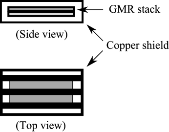
The use of a slitted copper enclosure greatly reduces the GMR sensitivity to magnetic field aligned perpendicular to the direction of the slits while perserving sensitivity to parallel magnetic fields. This holds only for high frequency magnetic fields and is due to the induced eddy currents that counter the external applied field.
V Apparatus
We now can put together a conceptual design for the atomic clock.
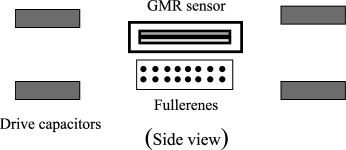
V.1 Atomic Clock Design
Putting together all the ingredients discussed above we have a micron-scale scheme that takes a drive voltage near the hyperfine resonance (driving the capacitors) and produces a small ( 1% of the drive field) signal that is detected and amplifed by the GMR sensor into a reasonable voltage. Exact device values are highly dependent upon materials and fabrication and won’t be calculated here. In terms of basic physics we expect a fullerene signal on resonance (413 MHz with a line width 1 Hertz) on the order of tesla and GMR sensors at room temperature have achieved a sensitivity of 350 pT/. Thus in a 1 Hertz filtered loop we should detect an atomic clock resonance with S/N 1.
V.2 Electronics

The above figure shows a simple oscillator design that will provide an ouput sine wave locked to the line frequency of the fullerene clock standard. The AGC circuit is designed to provide stable oscillations just below saturation. Starting from Power On, the intrinsic noise in the circuit will provide a nanovolt or so in the 1 Hz resonance bandwidth. If the amplifier ultimately provides a drive signal of around 1 volt with a mild amount of net circuit gain, we should have stable full-power operation in 100 system time constants, 100 x 1 sec (1/bandwidth). Faster turn on can be provided by strobing the input of the resonator with a pulse providing substantial fourier components near the resonance.
V.3 Clock Scalability
The simple scheme we’ve discussed gives us a micron-scale atomic clock with accuracy and a power dissipation of a nanowatt (10 nW capacitive drive but we can use resonant circuits to store the energy). This will likely be adequate for many mobile/sensor net applications but not adequate for more demanding situations. What can be done?
First, as GMR sensors improve (BMR, etc.), we can use more diluted fullerene stacks to gain a sharper line by a cubic factor in separation as we lose an equal amout of magnetic signal. A nanoscale-precise placing of fullerenes would give us a very well determined perturbation situation that can be exploited for accuracy. In the limit of true nanotechnology the ultimate clock is a single fullerene with considerable shielding. This should be competitive with very good atomic clocks of vastly more volume.
Appendix A Variance of Fullerene Electron-Nuclear Interaction
The idealized variation in frequency shift due to nearby endohedral fullerenes
density of fullerenes,
| (11) | |||||
| (12) |
| (13) |
Therefore
| (14) |
The expectation value for the nuclear frequency shift
| (15) |
| (16) |
| (17) |
| (18) |
| (20) | |||||
References
- [1] A. Abragam. Principles of Nuclear Magnetism, page 193.
- [2] A. Abragam. Principles of Nuclear Magnetism, page 46.
- [3] H. D. Chopra and S. Z. Hua. Phys. Rev. B, 66:20403, 2002.
- [4] David Culler. Private communication.
- [5] F. Diederich. Pure and Applied Chemistry, 69:395, 1997.
- [6] A. Ray et al. Change of decay rate in exohedral and endohedral fullerene compounds and its implications. arXiv:nucl-ex/0509021 v1, 2005.
- [7] A. Weidinger et al. Appl. Phys. A: Mater. Sci. Process., A66:287, 1998.
- [8] B. Goedde et al. Fullerenes for the New Millenium, page 304. The Electrochemical Society, 2001.
- [9] B. Pietzak et al. Chem. Phys. Lett., 279:259, 1997.
- [10] C. H. Tsang et al. IBM J. Res. Develop., 42:103, 1998.
- [11] M. Pannetier et al. Science, 304:1648, 2004.
- [12] M. Saunders et al. Science, 259:1428, 1993.
- [13] M. Waiblinger et al. Phys. Rev. B, 64:159901, 2001.
- [14] M. Waiblinger et al. Phys. Rev. B, 63:045421, 2001.
- [15] S. Stevenson et al. Nature (London), 401:55, 1999.
- [16] T. A. Murphy et al. Phys. Rev. Lett., 77:1075, 1998.
- [17] T. Ohtsuki et al. Phys. Rev. Lett., 93:112501–1, 2004.
- [18] W. Harneit. Phys. Rev. A., 65:032322, 2002.
- [19] S. V. Patwardhan et al. J. Inorganic and Organometallic Polymers, 12:49-55, 2002
- [20] S. E. Russek. IEEE Trans. Mag., 36:2560, 2000.
- [21] H. Shinohara. Rep. Prog. Phys., 63:843, 2000.
- [22] J. Twamley. Quantum cellular automata quantum computing with endohedral fullerenes arXiv:quant-ph/0210202, 2002.