Current-voltage characteristics of semiconductor/ferromagnet junctions in the spin blockade regime
Abstract
It was recently predicted [Phys. Rev. B 75, 193301 (2007)] that spin blockade may develop at nonmagnetic semiconductor/perfect ferromagnet junctions when the electron flow is directed from the semiconductor into the ferromagnet. Here we consider current-voltage characteristics of such junctions. By taking into account the contact resistance, we demonstrate a current stabilization effect: by increasing the applied voltage the current density through the junction saturates at a specific value. The transient behavior of the current density is also investigated.
There is currently a great deal of interest in spin-dependent transport phenomena in semiconductors and their junctions with ferromagnets review ; per ; Flatte ; saikin ; bleibaum ; rashba ; pershin ; r5 ; r6 ; r7 ; r8 ; r8a ; stephens ; crooker ; sham1 . In large part, this interest is motivated by the goal to exploit these phenomena in new technologies, such as spintronics and quantum computation review . Recently, some attention has been focused on the problem of the extraction of spin-polarized electrons from the semiconductor to the ferromagnet r8 ; r8a ; stephens ; crooker ; sham1 . Despite the apparent similarity of spin extraction with spin injection, spin extraction shows unique features. In particular, we have recently predicted per that the spin extraction process at nonmagnetic semiconductor/perfect ferromagnet junctions can be limited by spin blockade. The physical mechanism for spin blockade is the following: the outflow of majority-spin electrons from the semiconductor leaves a cloud of minority-spin electrons, which limits the majority-spin current through the junction.
In this letter we explore consequences of this phenomenon that can be easily verified experimentally. In particular, we study the current-voltage characteristics of such junctions. We do so by considering the conductivity of each of its components (semiconductor, ferromagnet and their contact). We show that the current flowing in a circuit involving a semiconductor/ferromagnet interface in the spin blockade regime saturates with increasing applied voltage. Therefore, such an interface can be potentially used as a spin-based current stabilizer. We also show that in structures with a semiconducting region longer that the spin diffusion length, the current density saturates to the critical current density found in Ref. per, . Instead, in junctions with the semiconductor region shorter than the spin diffusion length, the asymptotic current value mey be different from depending on how the semiconductor is connected from the opposite side of the junction. In particular, if this second contact is a good contact with a normal metal, then the asymptotic current value is higher than . We also consider transient processes, which, due to the finite response time of the spin polarization to the applied voltage, limit the speed of operation of such devices.
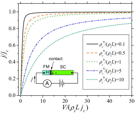
The circuit we have in mind is shown schematically in the inset of Fig. 1. We consider a voltage source (battery) connected to the semiconductor and ferromagnet regions of the junction. Assuming that the ferromagnet is a good conductor we can neglect the voltage drop across it. We also assume a good contact of the voltage source with the semiconductor (ohmic or nonlinear contact at this junction can be easily incorporated into our model). Therefore, there are two components of the total circuit where the voltage mainly drops: the semiconductor part, and its contact with the ferromagnet. We can then write the total applied voltage as , where and are voltage drops across the semiconductor region, and the contact, respectively. In our model, we consider a perfect ferromagnet, such as a half-metal ferromagnet. While both spin-up and spin-down electrons are injected from the battery into the semiconductor, only, let say, spin-up electrons are extracted from the semiconductor into the ferromagnet.
Spin and charge transport of a non-degenerate electron gas in the semiconductor can be conveniently described within the drift-diffusion approximation Flatte ; per . For simplicity, we neglect charge accumulation effects as in Ref. per, . In the semiconductor region we can then write
| (1) |
where is the current density, is the conductivity, is the electric field, is the mobility defined via , is the length of the semiconductor, and is the semiconductor resistivity. Next, we consider the voltage drop across the contact. The conductivity of the contact is proportional to the density of majority spin electrons in the semiconductor near the contact, . Therefore, assuming a linear relationship between the current and voltage drop across the contact at a fixed spin-up density, , we write
| (3) |
Eq. (3), which couples and , must be supplemented by the system of drift-diffusion equations for the semiconductor region whose solution gives . This system of equations consists of the continuity equations for spin-up and spin-down electrons, and the equations for the two spin currents:
| (4) |
| (5) |
It is assumed that the total electron density in the semiconductor is constant, i.e., . Correspondingly, the electric field is homogeneous and coupled to the total current density as . The boundary conditions are: , , .
In the following, we will consider separately the two cases of long () and short () semiconductor regions, with the spin diffusion length defined below.
(i) .— In this limit, a steady-state solution of Eqs. (4,5) is known per . The spin densities decay exponentially from the junction to their bulk values of . The decay occurs on the length scale of the up-stream spin-diffusion length Flatte ; per . The spin-up density at the junction is per
| (6) |
Substituting Eq. (6) into Eq. (3) and introducing the dimensionless current density , we get a closed equation coupling current density and voltage:
| (7) |
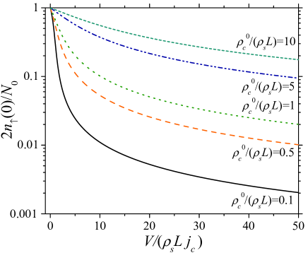
Fig. 1 shows solutions of Eq. (7) at different values of the ratio of the contact resistance to the resistance of the semiconductor region. All curves saturate at with increasing voltage. The saturation occurs faster in systems having smaller contact resistance. In Fig. 2, we plot the corresponding spin-up density . It follows from Figs. 1 and 2 that, for the selected values of parameters, the current density is quite close to the critical current density at voltages for which . For current stabilization applications, by specifying the maximum desired deviation of from , one can obtain the minimal voltage required for that deviation using Eq. (7) prec .
(ii) .— In this limit, Eqs. (4,5), supplemented by Eq. (3), were solved numerically numscheme . Starting with unpolarized electrons in the semiconductor, we have iterated at each time step Eqs. (4,5) with the constrain imposed by Eq. (3).
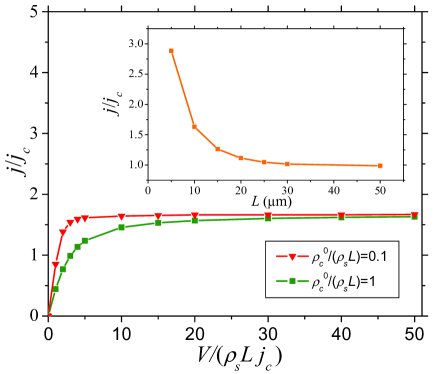
In this regime, the current-voltage characteristics have a similar saturation behavior as in the case . However, the asymptotic values of the current density (, ) are higher than (see Fig. 3). This is due to the boundary conditions . Such boundary condition describes a perfect contact of the semiconductor with a large reservoir of spin-unpolarized electrons. These spin-unpolarized electrons facilitate diffusion of electrons from the contact region, reducing the level of spin polarization near the contact and thus increasing the current density at which spin blockade occurs. We plot the current density as a function of in the inset of Fig. 3. For the selected set of parameters, the current density starts to deviate noticeably from in structures with m.
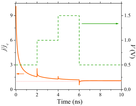
Finally, in view of potential applications, it is important to know the transient behavior of the current density. To do this, we consider stepwise voltage changes as shown in Fig. 4. This illustrative shape of was selected to show the response to both positive and negative voltage increments. The resultant current density depicted in Fig. 4 exhibits spikes at each change in . The main change in current density occurs during the first several hundreds of picoseconds after the voltage is applied. Physically, during this time period the electron spin polarization adjusts to a new value of the bias. In particular, immediately after an increase of , is larger than its steady-state value at the same voltage. Therefore, accordingly to Eq. (3), a positive spike in appears. Similarly, a stepwise decrease of results in a negative spike. We finally note that current density spikes can not be fitted by a single exponent.
This work is partly supported by the NSF Grant No. DMR-0133075.
References
- (1) I. Ẑutić, J. Fabian, and S. Das Sarma, Rev. Mod. Phys. 76, 323 (2004).
- (2) Y. V. Pershin and M. Di Ventra, Phys. Rev. B 75, 193301 (2007).
- (3) Z. G. Yu and M. E. Flatté, Phys. Rev. B 66, 201202(R) (2002).
- (4) M. Shen, S. Saikin, M.-C. Cheng, J. Appl. Phys. 96, 4319 (2004).
- (5) O. Bleibaum, Phys. Rev. B 73, 035322 (2006).
- (6) E. I. Rashba, Eur. Phys. J. B 29, 513 (2002).
- (7) Yu. V. Pershin, Phys. Rev. B 71, 155317 (2005); Yu. V. Pershin, Physica E 27, 77 (2005).
- (8) M. Q. Weng and M. W. Wu, Phys. Rev. B 66, 235109 (2002).
- (9) M. M. Glazov and E. L. Ivchenko, JETP Lett. 75, 403 (2002).
- (10) D. Csontos and S. E. Ulloa, Phys. Rev. B 74, 155207 (2006).
- (11) R.K. Kawakami, Y. Kato, M. Hanson, I. Malajovich, J. M. Stephens, E. Johnston-Halperin, G. Salis, A. C. Gossard, and D. D. Awschalom, Science 294, 131 (2001).
- (12) R. J. Epstein, I. Malajovich, R. K. Kawakami, Y. Chye, M. Hanson, P. M. Petroff, A. C. Gossard, and D. D. Awschalom, Phys. Rev. B 65, 121202(R) (2002).
- (13) J. Stephens, J. Berezovsky, J. P. McGuire, L. J. Sham, A. C. Gossard, and D. D. Awschalom, Phys. Rev. Lett. 93, 097602 (2004)
- (14) S. A. Crooker, M. Furis, X. Lou, C. Adelmann, D. L. Smith, C. J. Palmstrom, and P. A. Crowell, Science 309 2191, (2005).
- (15) H. Dery and L. J. Sham, Phys. Rev. Lett. 98, 046602 (2007).
- (16) We note that is linear in .
- (17) We have employed the Scharfetter-Gummel discretization scheme [D. L. Scharfetter and H. K. Gummel, IEEE. Trans. Electron. Devices, ED-16, 64 (1969)] to solve both Eqs. (4) and (5).