Setup for shot noise measurements in carbon nanotubes
Abstract
We have constructed a noise measurement setup for high impedance carbon nanotube samples. Our setup, working in the frequency range of 600 - 900 MHz, takes advantage of the fact that the shot noise power is reasonably large for high impedance sources so that relatively large, fixed non-matching conditions can be tolerated.
Keywords:
Carbon nanotubes, microwave frequency, shot noise:
73.23.-b, 73.23.Hk, 85.25.CpNoise measurements in out-of-equilibrium conditions can be employed to acquire extra information on top of that obtained from ordinary conductance measurements, the data of which are related to equilibrium noise by the fluctuation dissipation theorem. Such noise measurements, however, are hindered by the ubiquitous 1/f noise, in respect to which carbon nanotube devices make no exception. Collins et al. measured 1/ noise of several samples of single-walled nanotubes (SWNT), and found them to be so noisy that their use as electronic components is compromisedCollins , at least at room temperature. On the contrary, extremely good low-frequency noise properties have been achieved for single electron transistors made out of multiwalled carbon nanotubes (MWNT) by Roschier et al.free .
Altogether, on the basis of the noise measurements performed so far, it has become apparent that standard low-noise experimental techniques, reaching only up to 10 kHz due to cut-off problems, are not sufficient to study shot noise phenomena in carbon nanotubes. One approach to circumvent the limitations due to RC cut-off is to use resonant techniques to compensate the lead capacitance. Alternatively, microwave techniques with impedance matching may be employed. Both methods call for high-frequency, low temperature amplifiers, working in either the MHz or even the GHz regime. Our new noise measurement setup employs microwave techniques but differs slightly from the standard solution by allowing for unmatching conditions for the sample.
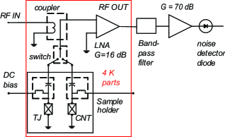
The heart of our setup is a cooled, home-made HEMT preamplifier that operates in the frequency range of range of 600 - 950 MHzLeifCryo04 . The average noise temperature of this low-noise amplifier (LNA) over the measurement bandwidth of 600-900 MHz is about 4 K. Under strong unmatching conditions, the back action noise of the preamplifier is fully reflected back to the amplifier, independent of the sample impedance, and therefore this gives only a constant shift in the level of integrated noise at the output. The setup is illustrated in Fig. 1.
The main goal in our setup is to measure reliably the Fano-factor which relates the measured noise to the full shot noise of a Poissonian process: , where is the average current. This is a characteristic number for mesoscopic samples in general BB . The Fano-factor is connected to quantum partition noise, which for a single transport channel is given by
| (1) |
where transmission coefficient is denoted by . In a multichannel system, sum over the transmission channels is taken. For example, for a mesoscopic diffusive wire, one obtains without interaction or hot electron effects. For a tunnel junction, . In fact, by having a high impedance tunnel junction and a microwave switch, this latter fact is employed to calibrate the sensitivity of our noise setup.
In our setup, bias-tees are used to allow voltage biasing of the sample and to measure the IV-characteristics while the noise measurement at microwave frequencies is going on. The amplification by the 4.2 K amplifier enhanced by three room-temperature amplifiers in series in order to make the signal level sufficient for a Schottky-diode power detector. Band width limitation is employed before the detector in order to cut off the extra noise due to the rather wide band width of the room temperature amplifiers (6 GHz for MITEQ SMC03 and 20 GHz for SMC05). Small AC-modulation is typically applied on top of the DC-bias so that drift in the noise level is eliminated by using lock-in techniques after detection. The full noise can then be obtained by numerical integration. This scheme, however, does not eliminate the drift in the gain of the amplifiers. Temperature stabilization of the LNAs, especially the room temperature ones, has been found to decrease this drift substantially.
The noise power of a source having an impedance is given by
| (2) |
This formula shows that the thermal noise and the shot noise are intermixed in a manner depending on the Fano-factor, which makes a separation of the contributions of thermal and shot noise complicated. Since the preamplifier is matched to a transmission line having the impedance of , the coupling from the source to the preamplifier is governed by the mismatch between the transmission line and the source. This is governed by reflection coefficient in which denotes the small-signal resistance of the sample at the operating point. Thus, the noise power coupled to the preamplifier becomes
| (3) |
where the latter form is valid in the regime . Therefore, for samples with only weakly non-linear IV-curves, the Fano factor can be obtained directly as the ratio of the slopes of the noise vs. current curves measured for the tunnel junction and the nanotube samples.
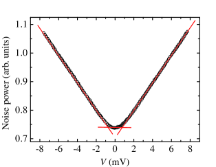
Fig. 2 illustrates the resolution achieved on a tunnel junction sample of resistance k. The signal to noise ratio is clearly so good that the main limitation of our method comes from the requirement of . As worked out by Spietz et al spietz04 , the cross-over regime between thermal and shot noise can be employed to determine absolute temperature of the sample, and by using the fitted lines we get K as expected.
References
- (1) P. G. Collins, M. S. Fuhrer, and A. Zettl, Appl. Phys. Lett. 76, 894 (2000).
- (2) L. Roschier, R. Tarkiainen, M. Ahlskog, M. Paalanen, and P. Hakonen, Appl. Phys. Lett. 78, 3295 (2001).
- (3) M. Ahlskog, R. Tarkiainen, L. Roschier, and P. Hakonen, Appl. Phys. Lett. 77, 4037 (2000).
- (4) H. W. Ch. Postma, T. F. Teepen, Z. Yao, and C. Dekker, in Electronic Correlations: from meso- to nanophysics, Proc. XXXVIth Rencontres de Moriond, ed. by T. Martin, G. Montambaux, and J. Trân Thanh Vân, EPD Sciences, France, 2001, pp. 433-436.
- (5) P.-E. Roche, M. Kociak, S. Guéron, A. Kasumov, B. Reulet, and H. Bouchiat, Eur. Phys. J. B 28, 217 (2002).
- (6) H. Ouacha, M. Willander, H. Y. Yu, Y. W. Park, M. S. Kabir, S. H. M. Persson, L. B. Kish, and A. Ouacha, Appl. Phys. Lett. 80, 1055 (2002).
- (7) E. S. Snow, J. P. Novak, M. D. Lay, and F. K. Perkins, Appl. Phys. Lett. 85, 4172 (2004).
- (8) R. Vajtai, B. Q. Wei, Z. J. Zhang, Y. Jung, G. Ramanath, and P. M. Ajayan, Smart Mater. Struct. 11, 691 (2002).
- (9) R. Tarkiainen, L. Roschier, M. Ahlskog, M. Paalanen, and P. Hakonen, Physica E 28, 57 (2005).
- (10) L. Roschier and P. Hakonen, Cryogenics, 44,783 (2004).
- (11) Ya.M. Blanter, M. Büttiker, Phys. Rep. 336, 1 (2000).
- (12) L. Spietz, K. W. Lehnert, I. Siddiqi, and R. J. Schoelkopf, Science 300, 1929 (2003).