Superconductivity in spinel oxide LiTi2O4 epitaxial thin films
Abstract
LiTi2O4 is a unique material in that it is the only known oxide spinel superconductor. Although bulk studies have demonstrated that superconductivity can be generally described by the Bardeen-Cooper-Schreiffer theory, the microscopic mechanisms of superconductivity are not yet resolved fully. The sensitivity of the superconducting properties to various defects of the spinel crystal structure provides insight into such mechanisms. Epitaxial films of LiTi2O4 on single crystalline substrates of MgAl2O4, MgO, and SrTiO3 provide model systems to systematically explore the effects of lattice strain and microstructural disorder. Lattice strain that affects bandwidth gives rise to limited variations in the superconducting and normal state properties. Microstructural disorder such as antiphase boundaries that give rise to Ti network disorder can reduce the critical temperature, but Ti network disorder combined with Mg interdiffusion can affect the superconducting state much more dramatically. Thickness dependent transport studies indicate a superconductor-insulator transition as a function of film thickness regardless of lattice strain and microstructure. In addition, surface sensitive X-ray absorption spectroscopy has identified Ti to retain site symmetry and average valence of the bulk material regardless of film thickness.
pacs:
74.78.-w, 61.10.HtI Introduction
Spinel structure oxides offer a wealth of electronic and magnetic ground states across a broad range of temperatures. Spinel oxides with transition metals on the octahedral sites exhibit ferromagnetism, antiferromagnetism, charge ordering, and other types of magnetic and electronic ordering depending on the average valence of the cations. However, there is only one known oxide spinel superconductor to date, LiTi2O4 (LTO), with a superconducting phase that persists up to 13 K. Johnston et al. found superconductivity in LTO as the end member of a solid solution of spinel-structure Li1+xTi2-xO4 (0x0.33).Johnston et al. (1973); Johnston (1976) In the Li spinels half-integral charge exists on each of the octahedral ions due to the monovalent nature of tetrahedrally coordinated Li. Unlike the layered structure of superconducting cuprates, LTO has 3D connectivity of edge-sharing TiO6 octahedra with average octahedral site valence of (equal amounts of Ti3+ and Ti4+). Oxygen deficient SrTiO3-δ and LTO both superconduct and both have mixed-valent Ti in octahedral coordination;Dejongh (1988) however, the Ti3+/Ti4+ ratio is 1.0 in LTO while there is significantly more Ti4+ in SrTiO3-δ.
Superconductivity and normal state properties of LTO can be largely explained in terms of a -band superconductor within the Bardeen-Cooper-Schreiffer (BCS) model.Sun et al. (2004); Tang et al. (2006) However, the microscopic mechanisms of superconductivity are still not well understood and open questions still remain as to the role of electron-electron correlations and spin fluctuations in determining some of its properties. Recent theoretical studies on the composition-driven metal-insulator transition for Li(M,Ti)2O4 with M=Li and Al Fazileh et al. (2004, 2006) postulate that electronic correlations are strong in these materials. Since a quantum site percolation model that reproduces noninteracting behavior does not successfully predict the details of the metal to insulator transition, they conclude that electronic correlations are significant in the LTO parent system as well as Li-excess and Al-doped LTO.
In bulk studies of primarily polycrystalline samples, there have been widely varying normal state and superconducting properties influenced by vacancies,Harrison et al. (1984) Li content, and Ti network disorder.Moshopoulou et al. (1993, 1994) Studies probing the effects of lattice strain on the superconductivity in bulk LTO have shown the application of hydrostatic pressure to increase the Debye temperature which in turn increases Tc as predicted by BCS theory, and such enhancement of Tc has been observed in both Li deficient and stoichiometric LTO samples.Lin et al. (1985); Shelton et al. (1976) There have been comparatively fewer bulk single crystal studies with systematic characterization of physical properties.
Epitaxial thin films of LTO are model systems for the systematic study of the role of lattice strain and microstructural disorder on superconducting properties. Epitaxial lattice strain gives rise to changes in the bandwidth that affect electron-electron correlations in many epitaxial thin film systems.Prellier et al. (2000); Angilella et al. (2002); Autier-Laurent et al. (2006) In addition, systematic variations in epitaxial film microstructural disorder may be obtained through the choice of substrate with lattice parameters not equal to the film lattice parameter due to changes in film growth mode or nucleation of dislocations and other defects.Henzler (1996) Such variation in microstructure can shed light on the various scattering processes that may or may not affect its superconducting properties. Finally, the choice of substrate orientation may provide insight into either intrinsic or strain-induced anisotropic film properties.Wu et al. (1991); Habermeier (2000) However, to date there has been no report of epitaxial thin film growth, although polycrystalline thin films have been synthesized by Inukai et al.Inukai et al. (1982); Inukai and Murakami (1985)
In this paper, we report on the successful synthesis and superconducting and normal state characterization of epitaxial LTO thin films on single crystalline MgAl2O4, MgO, and SrTiO3 substrates. By comparing the superconducting and normal state transport properties of LTO films on these three different substrates we are able to identify the role of lattice strain, Ti network disorder and stoichiometry on superconductivity. For example, misregistry and disorder at grain boundaries emerge in films grown on SrTiO3 and MgO due to coalescence of spinel LTO grains that have twice the unit cell of the underlying substrate, and such defects are referred to as antiphase boundaries. Antiphase boundary disorder has been well-characterized in spinel films grown on MgO substrates via transmission electron microscopy analysis.Hu et al. (2001); Eerenstein et al. (2002) These defects disrupt Ti-O-Ti octahedral bond ordering in an analogous manner to the disruption of Fe-O-Fe bond ordering in Fe3O4,Margulies et al. (1997); Voogt et al. (1998) and such Ti network disorder would influence carrier transport in LTO films. On the other hand, Mg interdiffusion combined with antiphase boundary-related Ti disorder has a much larger effect on both normal state and superconducting properties. Thickness dependent transport studies indicate a superconductor-insulator transition as a function of film thickness regardless of substrate. Surface sensitive X-ray absorption spectroscopy (XAS) has identified Ti to retain site symmetry and average valence of the bulk material.
II Experimental Methods
We have chosen to study epitaxial LTO films on MgAl2O4 (MAO), MgO, and SrTiO3 (STO) substrates. LTO films on MgO and STO substrates give rise to antiphase boundaries due to the lattice parameter of LTO being twice that of MgO and STO. These antiphase boundaries provide Ti network disorder in LTO films. A previous report indicated that diffusion of Mg into LTO could suppress the superconducting phase,Dalton and Kurmoo (1995) and in this case the source of Mg would be interdiffusion at the film-substrate interface. Substrates without Mg were used to confirm the trends found in thickness dependence studies on MAO substrates. LTO films on MAO and STO show minimal interdiffusion at the film-substrate interface while there is significant Mg diffusion on MgO substrates. Furthermore, each of these substrates placed the film under differing amounts of lattice strain through epitaxy.
Nominally stoichiometric LTO material prepared by solid-state reaction yields a lattice parameter of 0.8405 nm by powder X-ray analysis.Lambert et al. (1988) Films on MgO (lattice constant a = 0.42112 nm, film-substrate mismatch f = +0.21 ) are under slight tension, while films on MAO (a = 0.80831 nm, f = -3.82 ) are under compressive strain. Since other spinels have been shown to grow epitaxially on perovskite-structure substrates,Zheng et al. (2004); Chopdekar et al. (2004) LTO films were also grown on perovskite STO (a = 0.3905 nm, f = -7.07 ). The perovskite substrate promoted the growth of the spinel superconducting phase in spite of the high compressive strain and anti-phase boundaries due to the unit cell of LTO being twice a perovskite unit cell. MAO and STO substrates were chosen to perform a more extensive thickness dependence study on both (001) and (110) oriented substrates.
Epitaxial thin films of the normal spinel structure oxide LiTi2O4 were deposited via pulsed laser deposition on single crystalline (001) MgO, (001), (111) and (110) MAO, and TiO2 - terminated (001) and (110) STO with thickness ranging from 5nm to 1m. In contrast to more equilibrium techniques such as evaporation, pulsed laser deposition can enable growth of phases not stable or difficult to grow in bulk form. Stability issues in air and the so-called ‘aging effect’ were seen in previous samples of stoichiometric LTO,Inukai et al. (1981); Xu et al. (2003) thus the commercial target (Praxair Surface Technologies) was a mixture of the stable phases ramsdellite lithium titanium oxide (Li2Ti3O7)Buckley et al. (1982); Abrahams et al. (1989) and rutile titanium oxide (TiO2) to achieve a Li:Ti ratio of 1:2. Powder X-ray diffraction confirms the presence of these oxides in the target powder but no spinel-type phase reflections were found.
Substrate temperatures were held at 450-600 ∘C in a vacuum of better than 5x10⁻⁶ Torr to promote growth of the superconducting phase. Growth of films at elevated temperatures in 100 mTorr of pure oxygen or at 200 ∘C and below in vacuum yielded insulating films with no superconducting transition. Smooth films with low particulate density (less than 0.05 particles/m2) were produced with laser fluence of 1-2 J/cm2 and a repetition rate of 3 Hz, resulting in a deposition rate of approximately 0.03 nm per pulse.
Rutherford Backscattering Spectrometry (RBS) was used to evaluate both film thickness and composition. However, quantitative analysis of low-Z ions such as Li and O is difficult, and as such only Ti atom density and uniformity were obtained using this technique. X-ray diffraction both in -2 and 4-circle mode using Siemens D5000 diffractometers assessed film crystallinity and orientation.
Soft X-ray absorption spectroscopy (XAS) on the Ti L2,3 and O K edges of LTO films was performed at beamlines 4.0.2 Young et al. (2001) and 6.3.1 Nachimuthu et al. (2004) of the Lawrence Berkeley National Laboratory Advanced Light Source. X-ray absorption spectra for LTO films of thickness 15-300 nm were taken at room temperature in both normal and grazing incidences (the sample’s surface normal direction was collinear with the incoming photon direction and was tilted 60 degrees from the incoming photon direction, respectively). Reference spectra were measured on bare substrates as well as powder from the target material. Spectra were obtained by measuring total electron yield, monitoring the sample drain current as a function of photon energy. Electron yield detection is surface sensitive with a probing depth of 2-5 nm. The sample current was normalized to the incoming photon flux as measured using a gold mesh inserted in the beam path. The degree of linear polarization of the incoming X-ray flux was 991 for both beamlines. The lateral dimensions of the X-ray interaction area are much larger than the electron escape depth vertically, thus the measured signal averages over a large number of intragrain volume as well as grain boundaries.
Normal and superconducting-state magnetic properties were measured in a Quantum Design superconducting quantum interference device (SQUID) magnetometer. Magnetization measurements were performed with DC field applied both in the plane and out of the plane of the sample. To minimize sample flux trapping when cooling through Tc, the trapped flux in the SQUID magnetometer’s superconducting magnet was reduced to less than 0.28 Oe as calibrated by a 99.9 pure Dy2O3 sample. Transport was measured in a Quantum Design physical property measurement system (PPMS) modified with a Keithley 236 source-measure unit and HP3488A switching matrix. Resistivity and Hall measurements were performed both in the normal and superconducting state. DC and low frequency (f = 13.739 Hz) AC resistivity measurements were carried out in varying fields applied out of the plane of the sample from 2-380 K. Measurements in both cryostats were taken from room temperature to 2 K in fields of up to 5 T for SQUID magnetometry measurements and up to 7 T for transport measurements.
III Structure
Structural analysis indicated that films on all substrates were single-phase and single orientation spinel composition. X-ray diffraction in -2 geometry showed spinel phase reflections that were epitaxially matched to the single crystal substrate. No reflections from constituent phases from the target or polymorphs of TiO2 were observed. Films on MAO and STO under compressive strain exhibited elongation of the out-of-plane lattice parameter. For example, reciprocal lattice mapping of the film 444 reflection on STO(110) showed almost full relaxation of the film to bulk lattice parameters for film thickness greater than 100 nm, but only partial relaxation below 100 nm. Careful X-ray diffraction measurements indicated that the lattice parameters of LTO were elongated along the out-of-plane direction with up to 1.7 elongation from bulk for a 22 nm thick film on (001)MAO. This result suggests that biaxial compressive strains for ultrathin films are non-volume preserving and therefore may affect the Debye temperature and in turn the Tc. Films on MgO had reflections which overlay the substrate reflections to within the experimental resolution of the diffractometer, thus the films are under slight tension and show very little contraction of the out-of-plane lattice parameter.
Atomic force microscopy (AFM) indicated the low lattice mismatch between LTO and MgO gave rise to smooth films with an RMS roughness of 0.444 nm (or approximately half of a spinel unit cell) for a 100 nm thick film. However, rougher film morphology was seen on MAO substrates, with 1.6-2.6 nm RMS roughness for films of similar thickness. Films on STO had comparable roughness to those on MAO, and film grain size for both substrates at a deposition temperature of 450 ∘C or 600 ∘C was on average 100 nm. The rougher surface morphology was attributed to the larger epitaxial lattice mismatch and the accompanying full lattice relaxation. Since STO and MgO have approximately half the unit cell size of LTO, we expect antiphase boundaries in the LTO films on STO and MgO but not on MAO. Given the similarities of the STO and MAO samples, these antiphase boundaries appear not to affect the surface morphology. Films on (110) oriented substrates had elongated grains with an aspect ratio of 2:1 favoring the [10] in-plane axis as the fast-growth direction, as well as increased out of plane roughness compared to (001) oriented films. No measurable anisotropy or roughening compared to (001) films was measured on films grown on (111) oriented MAO, though the average grain size of 30 nm was smaller than grain sizes of (110) films with comparable thickness.
RBS analysis enabled us to probe the degree of interdiffusion of species at the film/substrate interface. Because of the difficulty in analyzing low Z ions such as Li and O, we focused on analyzing the uniformity of the atomic density of Ti from the LTO as well as the atomic species from the respective substrates. RBS analysis confirmed the interdiffusion of Mg into the LTO films deposited at 600 ∘C from MgO substrates with an approximate ratio of Mg to Ti of 0.25:2 assuming a uniform film stoichiometry, but no measurable interdiffusion for films on STO or MAO substrates to within the 5 accuracy of the measurement. XAS of Mg K and Al K edges of as-deposited films on MgO (peak to background of 1.25:1 for Mg K edge) as well as films annealed for 10 minutes at 450 ∘C in 500 mTorr O2 on MAO (peak to background of 1.07:1 for Mg K edge) confirm interface Mg diffusing from the substrate into the film during growth on MgO when compared to spectra of bare substrates found in the literature. Similarity of the aforementioned spectra to MgAl2O4 Mg K edge spectraBugaev et al. (2001) implies that the interdiffused Mg in LTO/MgO samples substitutes primarily into tetrahedrally coordinated sites. However, as-deposited films on MAO show little Mg at the surface, with a peak to background of approximately 1.01:1 for the Mg K edge.
IV Ti L2,3 and O K X-ray Absorption Spectroscopy
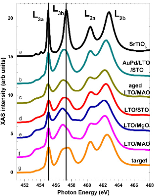
In order to probe the cation environment and its effect on the observation of superconductivity, surface sensitive soft X-ray absorption spectroscopy was performed at the Ti L2,3 and O K absorption edges on films of varying thickness below 500 nm to determine the Ti ion environment. Spectra have been aligned to the first sharp peak at each absorpton edge: 455 eV for the Ti L3a peak (Figure 1) and 530 eV for the first O K edge peak (Figure 2). Unlike heavier transition metals like Fe with two dominant features at the L2,3 edge, each of the Ti L3 (454-458 eV) and L2 (460-465 eV) absorption features are split into qualitatively t2g and eg-like sub-peaks. Crystal field effects have a large effect on the relative intensity of each of these peaks for the case of Ti4+ in different environments.de Groot et al. (1993, 1992) For the case of Ti3+ in compounds such as LaTiO3, the lower energy t2g-like peaks have low intensity compared to the eg-like peaks. Since bulk LTO has an equal number of Ti3+ and Ti4+ in octahedral environments, one would expect a spectrum similar to mixed-valence octahedral Ti such as in La1-ySryTiO3.Abbate et al. (1991) Comparison of the STO Ti4+-only spectrum in Figure 1 (a) to spectra (d)-(f) shows that LTO spectra have an increase in spectral weight at a 454 eV pre-peak feature at the expense of L3a intensity, as well as a merging of the L2a and L2b peaks. This trend is also seen in the y=0.4 and y=0.6 spectra from Abbate et al’s study on La1-ySryTiO3.Abbate et al. (1991)
Ra et al.Ra et al. (2004) examined powders of stoichiometric and Li-excess Li1+xTi2-xO4 and found qualitatively similar Ti L2,3 lineshapes for 0x0.33. Following their analysis, Lorentzian fits were made simultaneously to the pre-edge feature at 454 eV as well as each of the L3a, L3b, L2a, and L2b peaks. The ratio of L3a to L3b peak areas was approximately 0.14 for LTO on MgO and MAO, and showed a trend of increasing L3a contribution for films on STO and aged samples. This suggests that the surface of aged samples as well as the those of STO have slightly more Ti4+ character than similar films on MgO or MAO. Samples on STO capped with 3 nm AuPd or SrRuO3 deposited in-situ at 400 ∘C showed similar spectra to uncapped samples, suggesting that the more Ti4+-like spectrum is intrinsic to the surface and interface of as-deposited LTO films on STO.
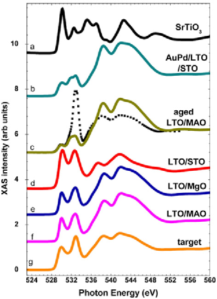
In contrast, the O K edge features may be divided into two regions: two low-energy peaks at 530 eV and 532.5 eV that show strong hybridization between O and Ti states, and a broader region between 536-548 eV exhibiting mixing of Ti and O states.de Groot et al. (1993) The lower-energy peaks for the various samples resemble the spectrum from the target material due to similar Ti-O hybridization with the intensity for the two peaks for the fresh samples equal in magnitude and insensitive to film thickness from 15 nm to 87 nm on STO. Since these lower-energy peaks are sensitive to neighboring Ti ions, one would expect similar spectra between the edge-sharing TiO6 octahedra in LTO and the distorted edge-sharing octahedra in ramsdellite Li2Ti3O7 and rutile TiO2 when compared to the corner-sharing octahedra in STO. One would also expect dramatic changes between fresh and aged sample spectra, but the aged LTO/MAO sample (Figure 2 (c)) showed large changes only when measured in grazing incidence. Grazing incidence measurements reduce the effective X-ray penetration depth by cos(), thus a very shallow volume is probed in grazing incidence. A similar but weaker trend of suppression of the 530 eV peak when compared to the 532.5 eV peak can be seen in the AuPd capped LTO/STO sample (Figure 2 (b)) as the AuPd cap also serves to reduce the effective probing depth of the LTO underlayer, but also protects the LTO material from reaction with air. Together these imply that while aging can affect the surface of LTO samples dramatically, the depth of aged material is on the order of the photoelectron escape depth (of order 5nmFrazer et al. (2003) but is material-dependent).
Again, comparison to the spectra from Ra et al. confirm that the surface material is close to target stoichiometry as-deposited and such surface material decreases in Li content as the sample ages. Aging for 48 hours in air affects the surface-sensitive XAS lineshape, but only with aging for longer timescales do significant changes in normal and superconducting state transport properties occur. Therefore the variations in transport properties for different samples described below cannot be attributed to variations in Ti average valence, Ti site symmetry or Li deficiency and hence Ti network disorder.
Although XAS spectra can show strong differences based on site symmetry for isovalent compounds such as rutile and anatase TiO2,de Groot et al. (1992) there is no clear distinction as a function of thickness for the LTO films shown in Figures 1 and 2. Thus the average valence and site occupation for the surface monolayers of each film should be identical, in spite of the presence of measurable superconductivity in thicker films and no resistive superconducting transition in a 15 nm film on STO. Thick and relaxed films on MAO, MgO and STO substrates also have similar features to the thin films on STO, indicating that the surface monolayers do not change substantially post-deposition as a function of substrate, and the XAS surface measurement is insensitive to the presence of anti-phase boundary disorder.
V Magnetism
The magnetic response of LTO films was measured on all substrates and found to be comparable to LTO bulk single crystals, polycrystalline pellets, and powder samples. Zero-field cooled samples at 1.8 K show diamagnetic shielding with low applied fields. A linear extrapolation at low applied fields for the data presented in Figure 3 yielded a typical lower critical field Hc1 of 463 Oe at which point the diamagnetic response deviated from linearity by 1 .
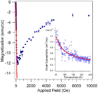
In order to understand the factors governing the normal state response of our films, we also measured the normal state susceptibility and fit it to a modified Curie-Weiss law.Johnston (1976) The Curie-Weiss behavior can result from trapped electrons on defect sites as well as impurities, whereas the weakly temperature dependent residual susceptibility in the model below is due to Pauli paramagnetism from conduction electrons as well as response from Ti3+-Ti3+ dimers.
| (1) |
Figure 3 inset shows the normal state susceptibility of a 400 nm LTO film on an STO substrate with the substrate background signal subtracted. A least-squares fit to the measured film susceptibility produced Curie constant Cm = 0.03980.001 cmK/mol and temperature = 13.62.1 K if the fit is constrained to match bulk values of Am = 0.00225 cm3/mol, and Bm = -9x10⁻⁸ cm3/molK for stoichiometric LTO.Harrison et al. (1985, 1984) A large uncertainty in the fit parameters for the temperature independent coefficient Am and linear temperature-dependent coefficient Bm are present if all parameters are left floating due to the film signal approaching the DC SQUID magnetometry noise floor of order 1x10⁻⁷ emu at 50,000 Oe. Localized electrons at oxygen defects have been shown to increase the paramagnetic response of LTO, and an upper limit of 10 of such impurities are present in the film assuming only trapped electrons of spin 1/2 are responsible for the entirety of the Curie-Weiss behavior.Harrison et al. (1984) For our LTO films which were grown in a reducing environment, the expected amount of oxygen defects per sample volume was larger than had been seen in previous bulk studies. In fact, the much larger surface to volume ratio and small grain size pointed to non-stoichiometry at the film surface and at grain boundaries. Accordingly, the Curie constant extracted from our DC susceptibility measurements showed an increase over that of previously measured bulk samples but were similar for our films on different substrates.
VI Transport
In order to probe the effects of lattice strain and microstructural disorder on the superconducting transition, we performed resistivity and Hall effect measurements on our LTO films. In particular, we discuss the normal state resistivity values, resistive transition temperatures and widths, the upper critical field, the Ginzburg-Landau coherence length-mean free path product and Hall mobility as a function of substrate and film thickness.
The normal-state resistivities versus temperature for nominally stoichiometric films on MAO (e.g. Figure 4) and STO deposited at 600 ∘C are comparable to that of polycrystalline thin film samplesInukai et al. (1982) as well as bulk polycrystalline samplesUeda et al. (1988) despite the presence of large compressive epitaxial strains. The film on (001) MAO described in Figure 4 as well as a film of comparable thickness on (001) STO both have a resistivity of 1.2x10cm at 12K. The similarity in magnitude of normal-state resistivity suggests that the presence of anti-phase boundaries, and hence Ti network disorder, in films on STO does not have a significant effect on the normal state transport in such LTO films. In contrast, films on MgO were found to have an order of magnitude greater normal-state resistivity despite having minimal epitaxial strain and much smoother film morphology compared to films on STO or MAO. The significantly larger normal state resistivity values suggest that partial Mg2+ interdiffusion into octahedral sublattice sitesLambert et al. (1988); Dalton and Kurmoo (1995); Steinbruck and Feltz (1992) at the 600 ∘C deposition temperature coupled with antiphase boundary-related Ti network disorderMoshopoulou et al. (1994) give rise to greater scattering in the normal state. A lower deposition temperature of 450 ∘C yielded films with higher residual resistivity, though superconducting transitions for films on MAO and STO remained at approximately 10 K. Interdiffusion does not play as large a role at a 450 ∘C deposition temperature as confirmed by an increase in the Mg K XAS edge intensity in films grown at 600 ∘C. Thus, the higher residual resistivity implies that scattering from defects such as anti-phase boundaries is increased for a given film thickness.
VI.1 Superconducting-State Transport
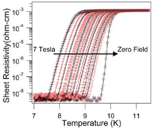
Figure 5 plots a summary of the resistive transition temperatures and widths measured for LTO films of varying thicknesses grown on different substrates and substrate orientations. Mirroring the trend observed with the normal state resistivity values, the films grown on (001) MAO and STO display similar behavior with a sharp zero field transition width (for 10 to 90 of normal state resistivity at 15 K) and transition temperature near 10.8 K. Nominally unstrained films on (001) MgO show a sharper zero field transition width of 0.3 K but with transition temperatures depressed to 6.9-9 K. The lower transition temperatures on MgO substrates, in contrast to those on MAO and STO substrates, can result from more significant Mg interdiffusion into the LTO film.Lambert et al. (1988) Films on (110) or (111) oriented MAO substrates show broader transition widths of up to 1.5 K which may be linked to smaller grain size in AFM scans. The increased number of non-superconducting grain boundaries in such samples may dominate the resistivity measurement, or the intragrain volumes themselves may be off-stoichiometry. Similar broadening of transition widths without significant degradation of the transition temperature were seen in powder pellets of LTOHarrison et al. (1985) as well as artificial YBa2Cu3O7 superlattices.Norton et al. (1991) The broadening in the aforementioned studies was not due to intrinsic properties of the superconducting regions but instead the boundary regions with the non-superconducting material. Since the LTO film transition temperature is not suppressed as a function of orientation for the 150 nm thick LTO films in Figure 5, this suggests that grain boundaries rather than whole-film non-stoichiometry is the source of the transition broadening. If the grain boundary resistance in LTO films can be a significant fraction of the measured resistance, careful analysis must be performed to measure intrinsic LTO properties from boundary effects as we will discuss in Section VI.2. Finally, films on STO have comparable transition temperatures to films on MAO, implying that antiphase boundaries have little effect on the magnitude of the critical temperature.
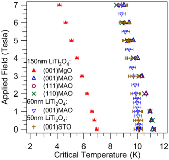
A closer look at the upper critical field and Ginzburg-Landau coherence length-mean free path product of LTO thin films on different substrates indicates the presence of a disordered phase either at the surface or film-substrate interface in thinner LTO samples. Using the Werthamer, Helfand and Hohemberg Werthamer et al. (1966) (WHH) model for a type II superconductor in the dirty limit, we can estimate the upper critical field () from the low-field slope of the critical temperature as a function of applied magnetic field. The extracted (T=0 K) values ranged from 12-24T for twenty-five samples depending on substrate choice and orientation, and the coherence length may be estimated from the Ginzburg-Landau formula as 3.5-5.5 nm which is consistent with bulk values. Foner and McNiffFoner and McNiff (1976) found that in spite of different starting compositions of Li2.6Ti2-zO4, Tc values were uniformly 12 K for stoichiometry deviations in the range of . However, there was strong variation in the quantities (d/dT) and , the zero-field slope of the vs Tc curve and the spin-orbit scattering parameter, respectively. In analogy, the Tc of films on MAO and STO for a given thickness is suppressed in thinner films to a value of on average 10.80.5 K compared to 900 nm thick films with a critical temperature of 11.3 K. Thinner films such as the 60 nm film on (001)MAO or 50 nm film on (001)STO in Figure 5 have suppressed critical temperatures in zero field, though in high field their behavior approaches those of thicker films. On the other hand, the films on MgO had a suppressed critical temperature but fit very well to the universal WHH curve when the reduced field = (T)/[Tc(H=0)(d/dT) ] is plotted as a function of reduced critical temperature t=Tc(H)/Tc(H=0). The increase in the reduced for low applied fields over that estimated from the WHH model can result from increased localization due to a disordered or inhomogeneous phase Coffey et al. (1984); Tenhover et al. (1981) in thinner LTO samples, whereas the significant interdiffusion of Mg in films on MgO yields a more uniform LiuMgvTi2O4 phase.
The Ginzburg-Landau coherence length-mean free path product may also be extracted from the transport data using the dirty-limit formula
| (2) |
For the resistive transitions plotted in Figure 5, for the 150 nm thick films is close to 1400 Å2 and is consistent with crystals at 5 or closer in composition to the stochiometric LiTi2O4 phase.Ueda et al. (1988); Sun et al. (2004) However, the 50 nm and 60 nm films on both MAO and STO have values close to 800 Å2, suggesting that deviations from bulk-like behavior at either the surface or the film-substrate interface dominate at these thicknesses.
VI.2 Normal-State Transport,
The Hall mobility of films on MAO and STO substrates was measured by computing the ratio between the Hall resistance and the sheet resistance in the van der Pauw configuration from the critical temperature up to room temperature. Assuming a simple one-carrier type model, films are n-type with carrier concentration of 1.3x1022 cm-3 for most films; this carrier concentration is equivalent to a single carrier per LTO formula unit as one would expect from the mixed-valent Ti ions. Carrier concentration and mobility were extracted by simultaneous van der Pauw and Hall measurements as a function of applied field out of the plane of the sample up to 7T between 11 K and 305 K.van der Pauw (1958)
Films deposited on STO and MAO at higher temperatures (600 ∘C) showed better crystallinity as confirmed by XRD rocking curves as well as mobility as high as 0.5 cm2/Vs at room temperature as measured by the Hall effect. Similar values for LTO mobility were found for polycrystalline sputtered LTO films annealed at 850 ∘C.Inukai and Murakami (1985) A suppression of mobility by a factor of 2 was seen in films deposited on STO at 450 ∘C, but the carrier concentration remained at 1 electron per LTO formula unit for films on STO at both 450 ∘C and 600 ∘C.
A detailed look at the normal state resistivity of LTO shows non-monotonic behavior with both positive and negative slope. Such features have been attributed to non-stoichiometry or substitution in LTO bulk samples.Steinbruck and Feltz (1992); Tang et al. (2006) As discussed in Section VI.1, grain boundary resistance may play a role in the measured sample resistance and thus must be taken into consideration when performing quantitative analysis on transport data. Thus, a two component model of resistivity consisting of metallic and semiconducting components was used to account for disorder and inhomogenieties in our thinner superconducting LTO films as well as films deposited at 450 ∘C. Similar modeling was successfully applied to (Ba,K)BiO3 films.Hellman and Hartford (1993)
| (3) |
The first bracketed term models the semiconducting component of the resistivity which freezes out at low temperatures, and is parametrized by the semiconducting channel resistivity asymptote and hopping activation energy . The second term models a metallic resistivity, and the weighting parameter details the relative contributions between the metallic and semiconducting channels. The normal-state resistivity has been fit in vanadium-silicon alloy filmsNava et al. (1986) using the electron-phonon scattering form of the Bloch-Gruneisen equation with a series residual resistivity as well as a phenomenological parallel saturation resistivity (equation 4). The Bloch-Gruneisen equation (equation 5) parameters include the high temperature resistivity coefficient and the Debye temperature . We may use this model for the metallic resistivity term in equation 3 for samples with non-monotonic resistivity, as well as only using equation 4 for samples with monotonic metallic resistivity such as 60 nm and thicker films on both MAO and STO substrates deposited at 600 ∘C.
| (4) |
| (5) |
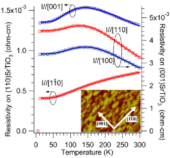
For samples that have monotonic resistivity with a positive temperature coefficient of resisitivty, such as the LTO/(110)STO I//[10] data in Figure 6, equation 4 may be used to obtain and . For a range of different sample thicknesses with non-monotonic resistivity, equation 3 is better suited to fit the data by leaving , , , , and floating during data fitting while constraining and to match values obtained from samples with monotonic resistivity.
Values for the LTO/(110)STO I//[10] data in Figure 6 when fit to equation 4 are = 4.6x10cm/K and = 420 K. The resulting Debye temperature of 420 K is suppressed compared to measured Debye temperature of 537-700 K via heat capacity experiments.Sun et al. (2004) Tang et al.Tang et al. (2006) assumed a closed-form solution of the Bloch-Gruneisen equation by assuming an Einstein phonon distribution, and their best fit Einstein temperature of 367 K is consistent with our best fit temperature of approximately 280 K with the same closed-form equation applied to the data in Figure 6.
If one compares the films on STO from Figure 6 and their twins on (001) and (110)MAO using the dimensionless weighting parameter , one may evaluate the relative contribution of the metallic and semiconducting components in the fit. Elongation of the grain structure for films on (110)STO (e.g. Figure 6) and MAO allows for the measurement of differing ratios of intragrain and intergrain volumes along different crystallographic directions in the same sample. Thus by using equation 3 one may separate the intrinsic LTO resistivity from contributions to the resistivity by non-intrinsic sources such as grain boundaries and other microstructural disorder. As the grains on (110)STO are elongated along the [10] direction, current confined along the [10] direction probes a large fraction of intragrain volumes with fewer intergrain areas contributing to the resistivity. On the other hand, when current is confined along the [001] in-plane direction for the same sample, the relative amount of intergrain resistivity contributions are increased, and accordingly the measured sheet resistivity increases as well as a decrease in resistivity with increasing temperature above 150K. This suggests that while intragrain volumes are well-connected along the [10] direction, grain boundary resistance can have substantial influence along the [001] crystallographic direction. The similarity in shape for the (001)STO resistivity data along both the [100] and [110] in-plane directions point to a more isotropic contribution of grain boundary resistance on the measured sheet resistivity.
For the above samples, falls between 1.0 (LTO on (110)STO with current along [10]) and 0.16 (LTO on (001)STO with current along [110]) suggesting that even in thick films the semiconducting channel is not negligible. Additionally, for films on STO and MAO confirms that there is little anisotropy in the ratio of the two resistivity channels along different crystallographic directions for (001) oriented films. Finally, indicates that antiphase boundaries in films on STO can increase the apparent contribution from a high resistivity channel in the temperature region of 20-100K for thick LTO films without substantially affecting the Tc.
VI.3 Normal-State Transport,
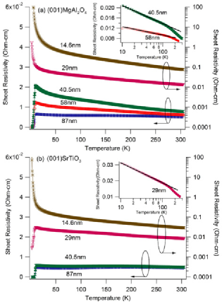
While films thicker than 100 nm on MAO and STO showed similar transport and magnetization characteristics, there was a distinct thickness dependence on the transport for films thinner than 100 nm. Figure 7 shows the normal state resistivities for LTO films on MAO and STO deposited at 450 ∘C with thickness ranging from 14.6 - 87 nm. The resistive superconducting transition in LTO films disappears for 29 nm thick LTO films on MAO and 14.6 nm thick films on STO.
The disappearance altogether of a superconducting transition in very thin LTO films is a signature of a superconductor-insulator transition as a function of film thickness. This transition has been seen in other systems and originated from Coulomb interactions or impurity scattering that localizes states.Bergmann (1982); Jaeger et al. (1986) The onset of insulating behavior occurs for thicker films in the case of LTO/MAO samples compared to those of LTO/STO, thus suggesting that the impurity scattering from interfacial defects such as misfit dislocationsMatthews and Blakeslee (1974) due to epitaxial strain between the film and the substrate in partially strained LTO/MAO are more effective in the suppression of superconductivity than misfit dislocations and antiphase boundaries in relaxed LTO/STO samples. However, with the exception of the thinnest films, the similarity in field dependent critical temperatures (Figure 5) indicates that such defects do not, for the most part, impact the superconducting properties.
A two component resistivity model may also be applied to LTO films thinner than 100 nm with high residual resistivity. However, in lieu of the Bloch-Gruneisen form of the metallic resistivity component, a logarithmic resistivity is better suited to the temperature regime between 15 K and 100 K (Figure 7, insets). Such a logarithmic dependence on temperature signifies either weak localization of carriers or defect and impurity-induced electron scattering as seen in granular or amorphous metal films.Deutscher et al. (1980); Bergmann (1982) A strong magnetoresistance is found for systems where weak localization is dominant,Bergmann (1982) but a weak magnetoresistance at 5 T of less than 0.1 % points to a defect-induced scattering mechanism such as antiphase boundary scattering as the source of logarithmic temperature dependence on resistance. As this logarithmic behavior is seen clearly in films on STO deposited at 450 ∘C ( Figure 7(b) 29 nm) but a Bloch-Gruneisen type fit is more suitable for films of the same thickness on STO deposited at 600 ∘C, the higher deposition temperature seems to reduces antiphase boundary defect density such that this scattering channel is minimized. Previous studies on films with antiphase boundaries have shown that high-temperature annealing results in grain growth and a reduction in antiphase boundary density.Venzke et al. (1996) A further crossover as a function of thickness from a logarithmic dependence to exponential temperature dependence of sheet resistance and stronger localization occurs for the thinnest films ( Figure 7 (a) or (b) 14.6 nm), and this normal-state resistance crossover is accompanied by a subsequent complete suppression of the superconducting transition. Such a crossover is seen in superconducting metal filmsDeutscher et al. (1980); Jaeger et al. (1989) at a normal-state sheet resistance around the value of the pair breaking resistance . This crossover occurs for LTO film sheet resistance values in the range of as determined by a linear extrapolation of the suppression of Tc as a function of sheet resistanceGraybeal and Beasley (1984) of films both on MAO and STO.
VII Conclusion
Epitaxial films of the spinel superconductor LiTi2O4 were grown on a variety of substrates to explore the effects of strain and microstructure on measured normal state and superconducting properties. Initial transport and magnetic measurements were consistent with bulk samples with an average critical temperature of 10.8 K and sharp transition width for films deposited on (001)MgAl2O4 and SrTiO3. The surface properties of freshly-deposited films on a variety of substrates were identical as measured by soft X-ray absorption spectroscopy on the Ti L2,3 edges, though substantial aging of the LTO samples can show a spectroscopic signature in the O K edge spectrum low energy 530 eV and 532.5 eV peaks. Detailed transport evaluation indicated that measured properties of the films were composed of contributions from metallic intragrain regions weighted with semiconducting grain boundary regions. Anti-phase boundaries have a strong anomalous effect on the magnetization of spinels oxides such as Fe3O4, but little if any contribution of this type of defect alone was seen when comparing the normal and superconducting transport and magnetic properties of films thicker than 100 nm deposited on perovskite SrTiO3 and isostructural spinel MgAl2O4-type substrates. By contrast, the interface Mg interdiffusion combined with antiphase boundaries in LTO films on MgO substrates gives rise to suppressed critical temperature accompanied by higher than bulk normal-state resistivity values. Comparison of the normal and superconducting state properties of LTO films on all three substrates indicate that lattice strain and hence bandwidth changes do not have a significant effect on the superconducting or normal state properties. Together these results indicate the robustness of the superconducting state of LiTi2O4 to lattice strain and microstructural disorder.
Acknowledgements.
The authors thank Prof. A. Stacy (UC Berkeley, Chemistry) for the use of her -2 diffractometer and K. M. Yu (Lawrence Berkeley Lab, Materials Science Division) for taking RBS spectra. Additional thanks to J.S. Bettinger and B. B. Nelson-Cheeseman for assistance in collecting XAS spectra. Thanks to Y. Matsushita, I.R. Fisher and M.R. Beasley (Stanford Univ, Applied Physics) for fruitful discussion, and Y. Takamura (University of California, Davis, Chemical Engineering and Materials Science) for insightful comments. This research was supported by the Office of Naval Research (N00014-97-1-0564) managed by Dr. Colin E.C. Wood. The Advanced Light Source is supported by the Director, Office of Science, Office of Basic Energy Sciences, of the U.S. Department of Energy under Contract No. DE-AC02-05CH11231.References
- Johnston et al. (1973) D. C. Johnston, H. Prakash, W. H. Zachariasen, and R. Viswanathan, Materials Research Bulletin 8, 777 (1973).
- Johnston (1976) D. C. Johnston, Journal of Low Temperature Physics 25, 145 (1976).
- Dejongh (1988) L. J. Dejongh, Physica C 152, 171 (1988).
- Sun et al. (2004) C. P. Sun, J. Y. Lin, S. Mollah, P. L. Ho, H. D. Yang, F. C. Hsu, Y. C. Liao, and M. K. Wu, Physical Review B 70, (2004).
- Tang et al. (2006) L. Tang, P. Y. Zou, L. Shan, A. F. Dong, G. C. Che, and H. H. Wen, Physical Review B 73, 184521 (2006).
- Fazileh et al. (2004) F. Fazileh, R. J. Gooding, and D. C. Johnston, Physical Review B 69, (2004).
- Fazileh et al. (2006) F. Fazileh, R. J. Gooding, W. A. Atkinson, and D. C. Johnston, Physical Review Letters 96, (2006).
- Harrison et al. (1984) M. R. Harrison, P. P. Edwards, and J. B. Goodenough, Journal of Solid State Chemistry 54, 136 (1984).
- Moshopoulou et al. (1993) E. Moshopoulou, P. Bordet, J. J. Capponi, C. Chaillout, B. Souletie, and A. Sulpice, Journal of Alloys and Compounds 195, 81 (1993).
- Moshopoulou et al. (1994) E. Moshopoulou, P. Bordet, A. Sulpice, and J. J. Capponi, Physica C 235, 747 (1994).
- Lin et al. (1985) J. H. Lin, T. H. Lin, and C. W. Chu, Journal of Low Temperature Physics 58, 363 (1985).
- Shelton et al. (1976) R. N. Shelton, D. C. Johnston, and H. Adrian, Solid State Communications 20, 1077 (1976).
- Prellier et al. (2000) W. Prellier, A. M. Haghiri-Gosnet, B. Mercey, P. Lecoeur, M. Hervieu, C. Simon, and B. Raveau, Applied Physics Letters 77, 1023 (2000).
- Angilella et al. (2002) G. G. N. Angilella, G. Balestrino, P. Cermelli, P. Podio-Guidugli, and A. A. Varlamov, The European Physical Journal B - Condensed Matter and Complex Systems 26, 67 (2002).
- Autier-Laurent et al. (2006) S. Autier-Laurent, B. Mercey, D. Chippaux, P. Limelette, and C. Simon, Physical Review B 74, 195109 (2006).
- Henzler (1996) M. Henzler, Surface Science 358, 809 (1996).
- Wu et al. (1991) J. Z. Wu, P. Y. Hsieh, A. V. McGuire, D. L. Schmidt, L. T. Wood, Y. Shen, and W. K. Chu, Phys. Rev. B 44, 12643 (1991).
- Habermeier (2000) H. U. Habermeier, Journal of Superconductivity 13, 871 (2000).
- Inukai et al. (1982) T. Inukai, T. Murakami, and T. Inamura, Thin Solid Films 94, 47 (1982).
- Inukai and Murakami (1985) T. Inukai and T. Murakami, Thin Solid Films 128, 275 (1985).
- Hu et al. (2001) G. Hu, V. G. Harris, and Y. Suzuki, IEEE Transactions on Magnetics 37, 2347 (2001).
- Eerenstein et al. (2002) W. Eerenstein, T. T. M. Palstra, T. Hibma, and S. Celotto, Phys. Rev. B 66, 201101 (2002).
- Margulies et al. (1997) D. T. Margulies, F. T. Parker, M. L. Rudee, F. E. Spada, J. N. Chapman, P. R. Aitchison, and A. E. Berkowitz, Physical Review Letters 79, 5162 (1997).
- Voogt et al. (1998) F. C. Voogt, T. T. M. Palstra, L. Niesen, O. C. Rogojanu, M. A. James, and T. Hibma, Phys. Rev. B 57, R8107 (1998).
- Dalton and Kurmoo (1995) M. Dalton and M. Kurmoo, Synthetic Metals 71, 1623 (1995).
- Lambert et al. (1988) P. M. Lambert, M. R. Harrison, and P. P. Edwards, Journal of Solid State Chemistry 75, 332 (1988).
- Zheng et al. (2004) H. Zheng, J. Wang, S. E. Lofland, Z. Ma, L. Mohaddes-Ardabili, T. Zhao, L. Salamanca-Riba, S. R. Shinde, S. B. Ogale, F. Bai, et al., Science 303, 661 (2004).
- Chopdekar et al. (2004) R. V. Chopdekar, G. Hu, A. C. Ford, and Y. Suzuki, Journal of Electronic Materials 33, 1254 (2004).
- Inukai et al. (1981) T. Inukai, T. Murakami, and T. Inamura, Japanese Journal of Applied Physics 20, L681 (1981).
- Xu et al. (2003) F. C. Xu, Y. C. Liao, M. J. Wang, C. T. Wu, K. F. Chiu, and M. K. Wu, Journal of Low Temperature Physics 131, 569 (2003).
- Buckley et al. (1982) R. G. Buckley, B. P. Clayman, and J. C. Mikkelsen, Physical Review B 26, 6509 (1982).
- Abrahams et al. (1989) I. Abrahams, P. G. Bruce, W. I. F. David, and A. R. West, Journal of Solid State Chemistry 78, 170 (1989).
- Young et al. (2001) A. T. Young, J. Feng, E. Arenholz, H. A. Padmore, T. Henderson, S. Marks, E. Hoyer, R. Schlueter, J. B. Kortright, V. Martynov, et al., Nuclear Instruments and Methods in Physics Research Section a-Accelerators Spectrometers Detectors and Associated Equipment 467, 549 (2001).
- Nachimuthu et al. (2004) P. Nachimuthu, J. H. Underwood, C. D. Kemp, E. M. Gullikson, D. W. Lindle, D. K. Shuh, and R. C. C. Perera, AIP Conference Proceedings: Eighth International Conference on Synchrotron Radiation Instrumentation 705, 454 (2004).
- Bugaev et al. (2001) L. A. Bugaev, A. P. Sokolenko, H. V. Dmitrienko, and A.-M. Flank, Phys. Rev. B 65, 024105 (2001).
- de Groot et al. (1993) F. M. F. de Groot, J. Faber, J. J. M. Michiels, M. T. Czyzyk, M. Abbate, and J. C. Fuggle, Physical Review B 48, 2074 (1993).
- de Groot et al. (1992) F. M. F. de Groot, M. O. Figueiredo, M. J. Basto, M. Abbate, H. Petersen, and J. C. Fuggle, Physics and Chemistry of Minerals 19, 140 (1992).
- Abbate et al. (1991) M. Abbate, F. M. F. de Groot, J. C. Fuggle, A. Fujimori, Y. Tokura, Y. Fujishima, O. Strebel, M. Domke, G. Kaindl, J. van Elp, et al., Physical Review B 44, 5419 (1991).
- Ra et al. (2004) W. Ra, M. Nakayama, H. Ikuta, Y. Uchimoto, and M. Wakihara, Applied Physics Letters 84, 4364 (2004).
- Frazer et al. (2003) B. H. Frazer, B. Gilbert, B. R. Sonderegger, and G. De Stasio, Surface Science 537, 161 (2003).
- Harrison et al. (1985) M. R. Harrison, P. P. Edwards, and J. B. Goodenough, Philosophical Magazine Part B 52, 679 (1985).
- Ueda et al. (1988) Y. Ueda, T. Tanaka, K. Kosuge, M. Ishikawa, and H. Yasuoka, Journal of Solid State Chemistry 77, 401 (1988).
- Steinbruck and Feltz (1992) M. Steinbruck and A. Feltz, Journal of Materials Science Letters 11, 216 (1992).
- Norton et al. (1991) D. P. Norton, D. H. Lowndes, S. J. Pennycook, and J. D. Budai, Physical Review Letters 67, 1358 (1991).
- Werthamer et al. (1966) N. Werthamer, E. Helfand, and P. Hohenberg, Physical Review 147, 295 (1966).
- Foner and McNiff (1976) S. Foner and J. McNiff, E. J., Solid State Communications 20, 995 (1976).
- Coffey et al. (1984) L. Coffey, K. A. Muttalib, and K. Levin, Physical Review Letters 52, 783 (1984).
- Tenhover et al. (1981) M. Tenhover, W. L. Johnson, and C. C. Tsuei, Solid State Communications 38, 53 (1981).
- van der Pauw (1958) L. J. van der Pauw, Philips Technical Review 20, 220 (1958).
- Hellman and Hartford (1993) E. S. Hellman and E. H. Hartford, Phys. Rev. B 47, 11346 (1993).
- Nava et al. (1986) F. Nava, O. Bisi, and K. N. Tu, Phys. Rev. B 34, 6143 (1986).
- Bergmann (1982) G. Bergmann, Phys. Rev. B 25, 2937 (1982).
- Jaeger et al. (1986) H. M. Jaeger, D. B. Haviland, A. M. Goldman, and B. G. Orr, Phys. Rev. B 34, 4920 (1986).
- Matthews and Blakeslee (1974) J. W. Matthews and A. E. Blakeslee, Journal of Crystal Growth 27, 118 (1974).
- Deutscher et al. (1980) G. Deutscher, B. Bandyopadhyay, T. Chui, P. Lindenfeld, W. L. McLean, and T. Worthington, Phys. Rev. Lett. 44, 1150 (1980).
- Venzke et al. (1996) S. Venzke, R. B. vanDover, J. M. Phillips, E. M. Gyory, T. Siegrist, C. H. Chen, D. Werder, R. M. Fleming, R. J. Felder, E. Coleman, et al., Journal of Materials Research 11, 1187 (1996).
- Jaeger et al. (1989) H. M. Jaeger, D. B. Haviland, B. G. Orr, and A. M. Goldman, Phys. Rev. B 40, 182 (1989).
- Graybeal and Beasley (1984) J. M. Graybeal and M. R. Beasley, Phys. Rev. B 29, 4167 (1984).