Huge negative differential conductance in Au-H2 molecular nanojunctions
Abstract
Experimental results showing huge negative differential conductance in gold-hydrogen molecular nanojunctions are presented. The results are analyzed in terms of two-level system (TLS) models: it is shown that a simple TLS model cannot produce peaklike structures in the differential conductance curves, whereas an asymmetrically coupled TLS model gives perfect fit to the data. Our analysis implies that the excitation of a bound molecule to a large number of energetically similar loosely bound states is responsible for the peaklike structures. Recent experimental studies showing related features are discussed within the framework of our model.
pacs:
73.63.Rt, 73.23.-b, 81.07.Nb, 85.65.+hI Introduction
The study of molecular nanojunctions built from simple molecules has attracted wide interest in recent years.agrait Contrary to more complex molecular electronics structures, the behaviour of some simple molecules bridging atomic-sized metallic junctions can already be understood in great detail, including the number of conductance channel analysis with conductance fluctuation and shot-noise measurements,smit ; djukicshotnoise the identification of various vibrational modes with point-contact spectroscopy djukic and the quantitative predictive power of computer simulations.thygesen The above methods were successfully used to describe platinum-hydrogen junctions: it was shown that a molecular hydrogen bridge with a single, perfectly transmitting channel is formed between the platinum electrodes.smit
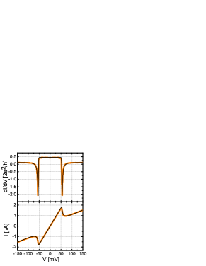
Point-contact spectroscopy turned out to be an especially useful tool in the study of molecular nanojunctions, as a fingerprint of the molecular vibrational modes can be given by simply identifying the small steplike signals in the curves of the junction.djukic However, the detection of the small vibrational signals is difficult for junctions with partially transmitting conductance channels, where quantum interference (QI) fluctuations may give an order of a magnitude larger signal.ludoph Surprisingly, instead of observing small steplike vibrational signals upon the background of QI fluctuations, molecular nanojunctions frequently show peaklike structures in the differential conductance curves with amplitudes comparable to or even much larger than the QI fluctuations. The peaks can be either positive or negative and their amplitude can be as small as a few percents, but – as we demonstrate in this manuscript – the peak-height can be several orders of magnitude larger showing a huge negative differential conductance (NDC) phenomenon (Fig. 1).
As a general feature of the phenomenon it can be stated that at low bias the conductance starts from a constant value, at a certain threshold voltage the peaklike structure is observed, and at higher bias the conductance saturates at a constant value again. The high-bias conductance plateau can be either higher or lower than the low-bias plateau. In the first case the peak at the transition energy is positive, whereas in the second case it is negative. In other words, the junction shows linear characteristics both at low and high biases but with a different slope, and at the threshold energy a sharp transition occurs between the two slopes. The switching of the conductance between two discrete levels implies the description of the phenomenon with a two-level system (TLS) model, but as we demonstrate in this paper a simple TLS model only gives steps in the at the excitation energy of the TLS, and it cannot account for sharp peaks.
The above phenomenon is not a unique feature of a special atomic configuration, but it frequently occurs in a wide conductance range and it appears almost in all the studied molecules and contact materials. In our experiments on gold-hydrogen molecular junctionscsonka we have recognized huge negative differential conductance curves in the conductance regime of G0 showing a characteristic threshold energy of meV. We have also observed similar phenomenon in niobium-hydrogen nanojunctions. In parallel the group of Jan van Ruitenbeek – focusing on the conductance range close to the quantum conductance unit – has demonstrated the occurrence of smaller peaklike structures.thijssen In their study the peaks appeared with H2, D2, O2, C2H2, CO, H2O and benzene as molecules, and Pt, Au, Ag and Ni as contact electrodes. An scanning tunneling microscopy (STM) study of a hydrogen-covered Cu surface revealed both sharp gaplike positive peaks and large negative differential conductance peaks in the tunneling regime.gupta The latter study has also demonstrated a clear telegraph fluctuation between the two levels on the millisecond timescale. An earlier STM study demonstrated smaller negative differential conductance peaks due to the conformational change of pyrrolidine molecule on copper surface.gaudioso
The above results imply the presence of a general physical phenomenon of molecular nanojunctions resulting in a similar feature under a wide range of experimental conditions. In Ref. thijssen, it was shown that in certain systems the peaklike structures are related to the vibrational modes of the molecular junctions and the observed features were successfully described in terms of a vibrationally mediated two-level transition model. This model, however, cannot describe the large negative differential conductance curves in our studies, and the large peaklike structures in the STM experiments.gupta
In the following, we present a detailed analysis of the observations in terms of two-level system models. We demonstrate the failure of a simple TLS model and the necessary ingredients for producing peaklike structures instead of simple conductance steps. We propose a model based on an asymmetrically coupled two-level system, which can describe all the above observations. The comparison of the model with experimental data implies a huge asymmetry in the coupling strength, which can be explained by exciting a strongly bound molecule to a large number of energetically similar loosely bound states. In our opinion, the proposed model is appropriate for describing the appearance of peaklike structures (or even negative differential conductance) in the curves of molecular nanojunctions under a wide range of experimental conditions.
II The failure of a simple two-level system model
The scattering on two-level systems in mesoscopic point-contacts has been widely studied after the discovery of point-contact spectroscopy (see Ref. halbritter, and references therein). In the following, based on the results for a general point-contact geometry,halbritter we shortly give an overview of the scattering process on a two-level system located near the center of an atomic-sized nanojunction. The TLS is considered as a double well potential, where the two states in the two potential wells have an energy difference (see Fig. 2). The two states are coupled by tunneling across the barrier with a coupling energy . The coupling between the wells causes a hybridization of the two states, resulting in two energy eigenvalues with a splitting of . It is considered that in the lower state of the TLS the contact has a conductance , whereas in the upper state the conductance is . The occupation number of the two states are denoted by and . These are time-averaged occupation numbers, the system is jumping between the two states showing a telegraph fluctuation. On a time-scale much longer than that of the TLS the fluctuation is averaged out, and the characteristic is determined by the voltage dependent occupation numbers:
| (1) | |||||
| (2) |
The occupation of the upper state can be calculated from the rate equation:
| (3) |
where the transition probabilities are determined by Fermi’s golden rule:
| (4) | |||
| (5) |
Here an electron from an occupied state with energy scatters on the TLS to an unoccupied state with energy . The nonequilibrium distribution function of the electrons is denoted by , whereas stands for the density of states at the Fermi energy. The transition matrix element from an initial electron state and the ground state of the TLS to a final electron state and the excited state of the TLS is considered as a constant coupling strength: . Assuming that the TLS is situated at the middle of the contact, where the half of the electrons is coming from the left and the half from the right electrode, the nonequilibrium distribution function can be approximated as:
| (6) |
where and are the equilibrium Fermi functions of the left and right electrodes, for which the chemical potential is shifted by the applied voltage. By inserting the distribution function to Eq. 4-5 and using the formula:
| (7) |
the rate equation can be written as:
| (8) |
where and are the inverse relaxation times of the lower and upper state of the TLS,
The steady state solution for the occupation number of the upper state is:
| (11) |
In the zero temperature limit the inverse relaxation times and the occupation number take the following simple forms:
| (14) | |||
| (17) | |||
| (20) |
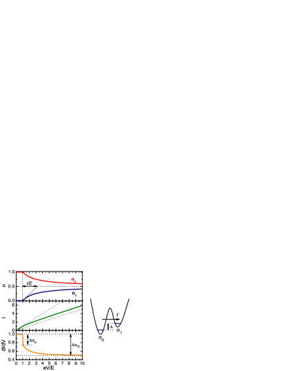
Fig. 2 shows the evolution of the occupation numbers, the curve and the differential conductance curve in the zero temperature limit. At both states are equally occupied with , but the transition towards this is very slow. A characteristic energy scale, for the variation of the occupation numbers can be defined by extrapolating the linear growth of at to the saturation value (see the upper panel in the figure). Due to the small slope of this characteristic energy scale is larger than the excitation energy, precisely: . This slow change is reflected by a smooth variation of the curve. The differential conductance curve shows a steplike change at , and then saturates to . The size of the step is smaller than the overall change of the conductance (), thus only a step and no peak is observed in the curve.
In the above considerations the calculation of the current (Eq. 1) includes only elastic scattering of the electrons on the two states of the TLS with different corresponding conductances, and the inelastic scattering processes are just setting the voltage dependence of the occupation numbers. However, the inelastic scattering of the electrons in principle gives direct contribution to the current: above the excitation energy the backscattering on the contact is enhanced due to the possibility for inelastic scattering. More precisely the inelastic current correction can be written as:
| (21) | |||
Here L+ and R- are incoming states to the contact on the left and right side, while R+ and L- are outgoing states, and e.g. is the probability that an electron from an incoming state on the left side excites the TLS and scatters to an outgoing state on the left side. The incoming states have the distribution function of the corresponding reservoir, while the distribution functions of the outgoing states are a mixture of the left and right Fermi functions with the transmission probability of the contact, :
![[Uncaptioned image]](/html/0706.2083/assets/x3.png)
The sign of the different current terms are determined by the direction of the outgoing states. After evaluating the energy integrals with the appropriate distribution functions one obtains:
| (22) |
where the first and second term correspond to the excitation and relaxation of the TLS, and:
The inelastic correction also causes a steplike change of the conductance, which has a magnitude of . For a contact with large transmission the conductance decreases at the excitation energy, while for a tunnel junction it increases, with a transition between the two cases at . We note that our simple model gives the same result for the transition between point-contact spectroscopy and inelastic electron tunneling spectroscopy at as more detailed calculations for vibrational spectroscopy signals.paulsson ; vega
The contribution of the inelastic process can easily be estimated. According to Eq. 17 the relaxation time of the TLS is , thus the inelastic correction to the conductance is . It means that a relaxation time of sec corresponds to an inelastic correction smaller than G0. In other words a correction of G0 would correspond to a TLS with a sub-picosecond relaxation time. These are unphysical numbers, especially if the telegraph fluctuation can be resolved, thus in the following the inelastic correction is neglected.
As a conclusion a simple TLS model cannot produce peaklike structures in the differential conductance curve. Regardless of the fine details of the model, for any TLS a characteristic energy is required for the transition, whereas for the observation of sharp peaks in the differential conductance is desired. As an other consequence of a simple TLS model, the high voltage conductance is limited by due to the equal population of the states at high bias. This contradicts the observation of Fig. 1, where . For such large change of the conductance a population inversion, is required.
III Two-level system model with asymmetric coupling
Both a population inversion and a sharp transition of the occupation numbers can be introduced by inserting an asymmetric coupling constant to the model, that is the coupling of the lower state of the TLS to the electrons in Eq. 4 is , whereas the coupling to the upper state in Eq. 5 is . The asymmetry parameter is defined as . With this modification, once the TLS can be excited, it cannot relax back easily, thus a sharp transition occurs.
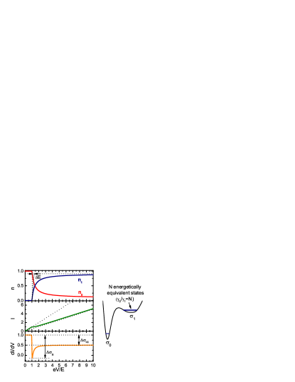
The original definition of the coupling constant does not allow any asymmetry, as due to the hermicity of the Hamilton operator. An asymmetry arises, however, if the phase spaces of the two levels are different. For instance if the ground state is well-defined, but the upper state is not a single level, but N energetically equivalent states (Fig. 3), then the effective coupling constant contains a summation for the final states resulting in .
With this modification the occupation numbers in the limit are defined by:
| (25) |
The corresponding occupation numbers, and curves are plotted in Fig. 3. The population inversion is obvious with . The characteristic energy of the variation of the occupation numbers is . The curve already shows a sharp transition from the initial to the final slope, and the differential conductance shows a sharp peak if the asymmetry parameter is high enough. The appearance of the peak is determined more precisely by calculating the ratio of and :
| (26) | |||||
| (27) |
With an asymmetry parameter a peak is observed in the differential conductance, whereas for smaller asymmetry only a steplike change arises. For a given difference in the conductances, both the width and the height of the conductance peak are determined by the asymmetry parameter, i.e. the peak width and the peak hight are not independent parameters. Depending on the sign of , the peak can be either positive or negative. The conductance at large bias is , thus it can be arbitrarily small compared to the zero-bias conductance.
At finite temperature the curve is calculated by inserting Eqs. II, II, 11 into Eq. 2 using asymmetric coupling constants, . The finite temperature causes a smearing of the curves, but the transition from steplike to peaklike structure is similarly observed at .
A more realistic generalization of the model can be given by assuming a distribution of the energy levels at the excited state with a density of states , for which the standard deviation () is kept much smaller than the mean value (). The asymmetry parameter is defined by the normalization: . With this modification the occupation of the excited states is energy dependent: , but the probability that any of the excited states is occupied is given by a single occupation number, . The calculation of the transition probability includes the integration of the excitation rate in Eq. II with the energy distribution:
| (28) |
The precise calculation of the relaxation probability () would require the knowledge of the energy dependent occupation number, . However, in the narrow neighborhood of the excitation energy, where the peak is observed the voltage dependence of the relaxation rate can be neglected beside the constant value of (see Eq. 17), thus the original formula for (Eq. II) is a good approximation for the finite distribution of the levels as well. Our analysis shows, that the relaxation rate can even be replaced by a voltage independent spontaneous relaxation rate without causing significant changes in the results.
As demonstrated in the following a TLS model with an asymmetry parameter, , and a narrow width of the upper states, , shows perfect agreement with the experimental observations.
IV Experimental results
In the following we present our experimental results on the negative differential conductance phenomenon in gold-hydrogen nanojunctions. The high stability atomic sized Au junctions were created by low-temperature mechanically controllable break junction technique. The hydrogen molecules were directed to the junction from a high purity source through a capillary in the sample holder. The molecules were dosed by opening a solenoid needle valve with short voltage pulses, adding a typical amount of mol of hydrogen molecules.
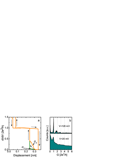
The appearance of the NDC phenomenon cannot be generally attributed to definite parts of the conductance traces, but in Au-H2 junctions the NDC curves were quite frequently observed when the junction was closed after complete disconnection, as demonstrated by the trace in Fig. 4a. The conductance curve was measured by recording a large number of curves during a single opening – closing cycle, and extracting the differential conductance values both at zero bias and at mV. During the opening of the junctions no difference is observed, but during the closing of the junction the two curves show large deviation. The high bias trace resembles the traditional traces of pure gold junctions: during the approach of the electrodes an exponential-like growth is observed, but already at a small conductance value ( G0) the junctions jumps to a direct contact with G0. At low bias voltage the conductance grows to a much higher value ( G0) before the jump to direct contact. The behavior of the conductance trace in Fig. 4a agrees with the general trend shown by the conductance histograms (Fig. 4b): at low bias a large variety of configurations is observed at any conductance value, whereas at high bias the weight in the region G0 is very small. Note that only a part of the configurations (a few percent of all traces) show NDC features, for other configurations irreversible jumps are observed in the curve at a certain threshold voltage. We have not found any evidence that the gold-hydrogen chains reported in our previous workcsonka would show NDC phenomenon or any peaklike structures in the differential conductance curve.
Figure 1 has already presented an example of the huge negative differential conductance phenomenon. Using the finite temperature results of the asymmetrically coupled TLS model with a Dirac-delta distribution of the levels () we have fitted our experimental data in Fig. 1. The fitting parameters are the energy, the temperature and the asymmetry parameter, whereas and are directly read from the experimental curve. As shown by the black solid lines in the figure, the model provides perfect fit to the data. The striking result of the fitting is the extremely large asymmetry parameter, .
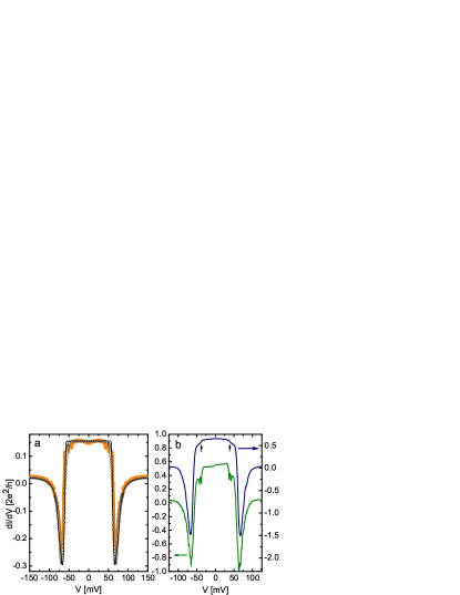
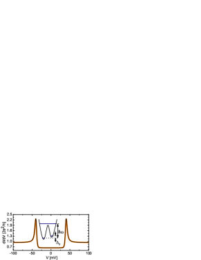
Figure 5a shows an other example for the NDC phenomenon. For this curve the fitting with a Dirac-delta distribution provides a nonrealistic temperature of K. By fitting with a finite width uniform distributionnote1 of the excitation levels the temperature can be kept at the experimental value ( K) resulting in a standard deviation of the upper states of meV. Fig. 5b shows further experimental curves exhibiting smaller features between the negative differential conductance peaks. In some measurements additional peaks appeared beside the main NDC peaks, which is demonstrated by the lower curve in the figure showing two smaller peaks at and meV. These observations could be explained by introducing further energy levels with different degeneracy, but such a model would be too much complicated without aiding the understanding of the general phenomenon. The upper curve shows a steplike decrease of at meV resembling the vibrational signal of molecular junctions, although its amplitude is rather large for a vibrational spectrum. (The typical conductance change due to vibrational excitations is at the conductance quantum,djukic and it should vanish towards G0, where the negative point-contact spectroscopy signal turns to positive inelastic electron tunneling spectroscopy signal.paulsson ; vega ) The observed steps could also be explained by the scattering on a symmetrically coupled TLS, for which the step-size can be as large as of the zero bias conductance.
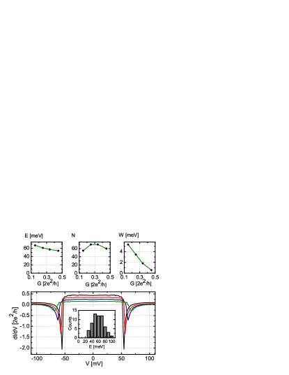
The bottom panel in Fig. 6 shows the variation of the negative differential conductance curves by changing the electrode separation. The curves were recorded during the closing of a disconnected junction, similarly to the trace in Fig. 4a. The upper panels present the change of the fitting parameters as a function of the zero bias conductance. Both the excitation energy, and the width of the excited levels, decrease with increasing conductance, whereas the asymmetry parameter, varies around a constant value.
We have repeated our measurements for a large amount of curves showing NDC feature. The observed excitation energies have shown a broad distribution in the range meV, as demonstrated by the inset in tho bottom panel of Fig. 6. Below meV we have not observed any peaks, whereas above meV the junctions frequently become unstable, and the recording of reproducible curves is not possible. In every case when the electrode separation dependence was studied was decreasing by increasing zero-bias conductance showing a shift of the excitation energy by even a few tens of millivolts. The standard deviation of the excited levels was typically in the range meV, also showing a decreasing tendency with increasing conductance. The asymmetry parameter was in the range . Note that with these parameters the average spacing of the excitation energies is smaller than the temperature smearing, thus the assumption for the continuous distribution of the levels is correct.
In our experiments the NDC curves on gold-hydrogen junctions have not shown any telegraph noise within the bandwidth of our setup ( kHz).
V Discussion
Our analysis of the two-level system models shows that in the case of two single levels the population of the upper level remains very small in the narrow neighborhood of the excitation energy, which inhibits the appearance of sharp peaklike structures in the differential conductance curve. By introducing a large asymmetry in the coupling constants, already a small voltage bias above the excitation energy causes a sudden flip of the occupation numbers, resulting in peaks or even huge negative differential conductance in the curves.
The analysis of our experimental curves shows that the negative differential conductance phenomenon is successfully fitted by the asymmetrically coupled TLS model, yielding extremely large asymmetry parameters (). This result implies, that the molecular contact has a ground state with a well-defined molecular configuration, from which it can be excited to a large number of energetically similar excited states. A trivial explanation would be the desorption of a bound molecule to the vacuum, however it is hard to imagine, that after complete desorption a molecule always returns to exactly the same bound-state. As a more realistic explanation, a strongly bound molecule is excited into a large number of energetically similar loosely bound states, from which it can relax to the original bound state.
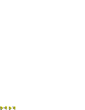
A possible illustration is presented in Fig. 7. In the ground state the molecule is strongly bound between the electrodes, whereas the excited states are loosely bound configurations where e.g. different angles of the molecule with respect to the contact axis have similar binding energy, and also the molecule can diffuse to different sites at the side of the junction. This picture is consistent with the conductance trace in Fig. 4: at low bias the molecular contact is dominating the conductance, whereas at high bias the molecule is kicked out to the side of the contact, and the conductance trace resembles the behavior of pure gold junctions. It is noted though, that the peaklike structures are observed with a large diversity of conditions, so in general Fig. 7 is regarded only as an illustrative picture
The conclusive message of the analysis is, that the desorption of a strongly bound molecule to a large number of energetically similar loosely bound states causes peaklike structures or even huge negative differential conductance in the curves. From the fitting of the experimental curves only the large asymmetry parameter can be deduced, but the precise microscopic origin of the asymmetry cannot be determined without detailed microscopic calculations. Possible candidates are the different arrangements and rotational states of the molecule with respect to the contact, but it is also very much probable, that the bound molecule is desorbed to different positions on the side of the contact, and then it can even diffuse away on the contact surface. In the latter case not necessarily the same molecule relaxes back to the initial bound state. All the above processes cause an effective asymmetry in the coupling.
Similar results were obtained on tunnel junctions with higher resistance in Ref. gupta, , where a hydrogen-covered Cu surface is studied with an STM tip. The authors present a phenomenological two-state model, which gives perfect fit to the data, but the microscopic parameters are hidden in the model, and for the more detailed understanding of the results further analysis is required. The fitting with our asymmetrically coupled TLS model shows that the experimental curves in Ref. gupta, correspond to similarly large asymmetry parameters. In the case of an STM geometry a direct picture can be associated with the asymmetry: a molecule bound between the surface and the tip can be excited to several equivalent states on other sites of the surface, away from the tip. The observation of the voltage dependent telegraph noise in Ref. gupta, provides a direct measure of the occupation numbers, proving the population inversion in the system.
The group of Jan van Ruitenbeek has demonstrated peaklike structures concentrating on contacts close to the conductance unit.thijssen ; djukicthesis In this conductance range the relative amplitudes of the peaks are much smaller than our NDC curves in the lower conductance regime, but the overall shape of the curves is similar. In some cases a direct transition from a steplike vibrational signal to a peaklike structure was observed, which implies the coupling of the phenomenon to molecular vibrations. The coupling to the vibrational modes was also indicated by the isotope shift of the peak positions. A TLS model illustrated in the inset of Fig. 8 was proposed, in which the two base levels of the double well potential (with a splitting of ) are separated by a wide potential well, which cannot be crossed. In both wells, however, a vibrational mode of the molecule can be excited (with ), and at the vibrational level the potential barrier can already be crossed, causing a hybridization of the excited levels between the two wells. In this model the upper base level is unoccupied for , but above the excitation energy the transition between the two wells is possible, and for the upper base level suddenly becomes almost half occupied above the excitation energy. Similarly to the asymmetrically coupled TLS model, this vibrationally mediated TLS model produces sharp peaklike structures in the due to the sudden change of the occupation numbers. The authors claim that the coupling of a vibrational mode to a TLS magnifies the otherwise tiny vibrational signal, and thus the sharp peaks directly show the vibrational modes of the junction.
Our analysis shows that the asymmetrically coupled TLS model proposed by us gives almost identical fits to the experimental curves in Ref. thijssen, as the vibrationally mediated TLS model, which means that the automatic identification of the peaklike structures with the vibrational modes of the junction is only possible if their growth from a vibrational spectrum is detected, and so the vibrational signal is anyhow resolved. In contrast, the negative differential curves demonstrated in our manuscript cannot be fitted with the model in Ref. thijssen, due to the large ratio of (). The authors use a symmetric coupling of the two levels, thus for moderate voltages (), and for high bias (), where the third level starts to be populated as well. The model could be generalized by inserting asymmetric coupling, however in this case the inclusion of the vibrational level is not necessary any more for fitting the curves. The broad distribution of the NDC peak positions also indicates that the phenomenon is not related to vibrational energies.
In our view the vibrationally mediated TLS model requires unique circumstances: the molecule needs to be really incorporated in the junction with well-defined vibrational energies. Furthermore, two similar configurations are required, which have the same vibrational energy, and for which the transition is only possible in the excited state. This phenomenon may be general in certain well-defined molecular junctions, for which the transition of a vibrational-like signal to a peaklike structure and the isotope shift of the peaks provides support. In contrast, the asymmetrically coupled TLS model can be imagined under a much broader range of experimental conditions, just a bound molecular configuration and a large number of energetically similar loosely bound (e.g. desorbed) states are required with some difference in the conductance. The fine details of the underlying physical phenomena may differ from system to system, however both models provide an illustration of a physical process that may lead to the appearance of peaklike structures in curves of molecular junctions.
VI Conclusions
In conclusion, we have shown that gold-hydrogen nanojunctions exhibit huge negative differential conductance in the conductance range of G0. The position of the peaks shows a broad distribution in the energy range meV. Similar features were observed in tunnel junctions with higher resistance using an STM setup,gupta whereas in break-junctions with G0 peaklike structures with smaller amplitude were detected.thijssen These results show that sharp peaklike structures are generally observed in the differential conductance curves of molecular nanojunctions under a wide range of experimental conditions: using different molecules, different electrode material and different contact sizes. All these experimental results imply the explanation of the observations in terms of two-level system models.
We have shown that a simple two-level system model cannot produce peaklike structures, but a TLS model with asymmetric coupling successfully fits all the experimental data. Our analysis shows that the peaklike curves correspond to large asymmetry parameters, which implies that a molecule from a bound state is excited to a large number of energetically similar loosely bound states. This picture provides a physical phenomenon that can appear under a wide range of experimental conditions and may explain the frequent occurrence of peaklike structures in curves of various molecular systems.
Our analysis also shows that a recently proposed vibrationally mediated two-level system modelthijssen ; djukicthesis may be applicable for certain well-defined molecular configurations, but the general relation of the conductance peaks to vibrational modes is not possible without further experimental evidences.
ACKNOWLEDGEMENTS
This work has been supported by the Hungarian research funds OTKA F049330, TS049881. A. Halbritter is a grantee of the Bolyai János Scholarship.
References
- (1) N. Agrait, A.L. Yeyati, J.M. van Ruitenbeek, Physics Reports 377, 81-279 (2003).
- (2) R.H.M. Smit, Y. Noat, C. Untiedt, N.D. Lang, M.C. van Hemert, J.M. van Ruitenbeek, Nature 419 906 (2002).
- (3) D. Djukic and J.M. van Ruitenbeek, Nano Letters, 6 789 (2006).
- (4) D. Djukic, K.S. Thygesen, C. Untiedt, R.H.M. Smit, K.W. Jacobsen, J.M. van Ruitenbeek, Phys. Rev. B. 71, 161402(R) (2005).
- (5) K.S. Thygesen, K.W. Jacobsen, Phys. Rev. Lett. 94 036807 (2005).
- (6) B. Ludoph and J.M. van Ruitenbeek, Phys. Rev. B. 61 2273 (2000); B. Ludoph, M.H. Devoret, D. Esteve, C. Urbina and J.M. van Ruitenbeek, Phys. Rev. Lett. 82 1530 (1999).
- (7) Sz. Csonka, A. Halbritter, and G. Mihály, Phys. Rev. B 73, 075405 (2006).
- (8) W.H.A. Thijssen, D. Djukic, A.F. Otte, R.H. Bremmer, J.M. van Ruitenbeek, Phys. Rev. Lett. 97, 226806 (2006)
- (9) J.A. Gupta, C.P. Lutz, A.J. Heinrich, D.M. Eigler, Phys. Rev. B. 71, 115416 (2005).
- (10) J. Gaudioso, L. J. Lauhon, and W. Ho Phys. Rev. Lett. 85, 1918 (2000).
- (11) A. Halbritter, L. Borda, A. Zawadowski, Advances in Physics 53, 939-1010 (2004).
- (12) M. Paulsson, T. Frederiksen, M. Brandbyge, Phys. Rev. B. 72, 201101(R) (2005).
- (13) L. de la Vega, A. Martin-Rodero, N. Agrait, A.L. Yeyati, Phys. Rev. B. 73, 075428 (2006).
- (14) We have found that the model is not sensitive to the choice of the distribution, all the distributions with a well-defined width (e.g. Gaussian) provide similar results. Note, that according to the general definition is always the standard deviation and not the width of the distribution.
- (15) D. Djukic, PhD thesis, Universiteit Leiden (2006).