Electronic transport in normal-conductor/graphene/normal-conductor junctions and conditions for insulating behavior at a finite charge-carrier density
Abstract
We investigate the conductance of normal-conductor/graphene/normal-conductor (NGN) junctions for arbitrary on-site potentials in the normal and graphitic parts of the system. We find that a ballistic NGN junction can display insulating behavior even when the charge-carrier density in the graphene part is finite. This effect originates in the different intervals supporting propagating modes in graphene and a normal conductor, and persists for moderate levels of bulk, edge or interface disorder. The ensuing conductance thresholds could be used as an electronic tool to map out details of the graphene band structure in absolute -space.
pacs:
73.63.-b, 72.10.Bg, 73.63.Bd, 81.05.UwI Introduction
Graphene, the two-dimensional arrangement of carbon atoms on a honeycomb lattice that has recently become available through ground-breaking fabrication methods, Novoselov2004 ; Geim2007 possesses a wide range of unique electronic transport properties which originate from the conical dispersion relation around the corners (K-points) of the hexagonal Brillouin zone. dresselhausbook The low-energy theory in the vicinity of these points is of the form of a Dirac equation for massless, chiral fermions. dirac1 The intrinsic transport properties studied on the basis of the Dirac equation (such as the quantum Hall effect, Novoselov2005 ; Zhang2005 ; Novoselov2006 ; roomtempqhe the minimal conductivity, Novoselov2005 ; Zhang2005 ; ludwig ; shon ; guinea1 ; tworzydlo ; Nomura ; aleiner ; altland ; ryu ; Ostrovsky ; DasSarma and weak localization corrections to the conductance Morozov ; Savchenko ; Wu ; mccann ; kechedzhi ; morpurgo ) therefore effectively probe the graphene band structure via the momentum difference relative to the K-points. On the other hand, detailed information corroborating the conical band structure in absolute space has recently become accessible via angle-resolved photoemission spectroscopy. arpes1 ; arpes2
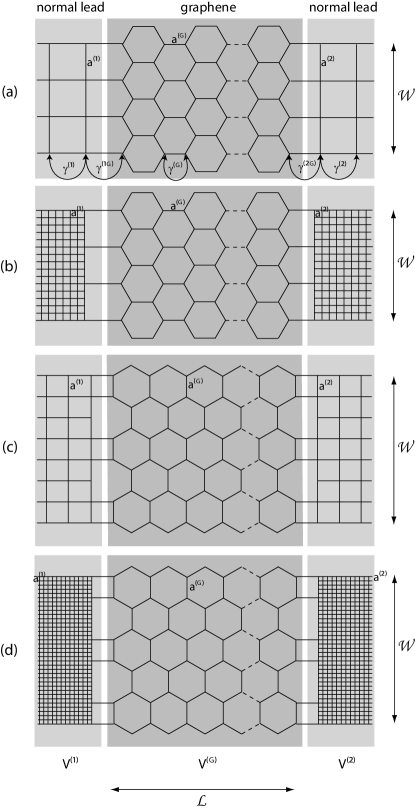
Recent theoretical transport studies have pointed out that highly unconventional devices could be fabricated in patterned and gated samples of graphene, such as Veselago lenses veselago and filters for the valley degree of freedom. valleyvalve These effects already occur in simple, rectangular graphitic samples, so-called nanoribbons, which have been studied in great detail in the past. Fujita ; Nakada ; Wakabayashi ; Miyamoto ; brey ; Ezawa ; Sasaki ; guinea2 ; guinea3 With few exceptions, however, theoretical investigations of electronic transport have concentrated on all-graphitic structures. In experiments, the ultimate electronic contacts are metallic (for illustration see, e.g., Ref. Huard, ). Two recent works schomerus ; blanter have addressed the coupling of graphene to normal-conducting electrodes, in each case considering normal-conductor/graphene/normal-conductor (NGN) junctions with an armchair ribbon and zigzag interfaces, as shown Fig. 1(a). In Ref. schomerus, , the graphitic part was fixed at the value of charge-neutral graphene, while the on-site potential in the leads was changed (the results were then compared to the results for a set-up in which the leads are also graphitic tworzydlo ). In Ref. blanter, , the on-site potential in all three regions was changed simultaneously (the resulting finite charge-carrier density in the graphitic part greatly enhances the conductance of the junction).
In this paper we systematically investigate the dependence of the electronic transport through NGN junctions on independent on-site potentials in the leads and in the graphitic region. Since the transport at finite charge-carrier density is anisotropic and depends on the details of the normal electrodes, we also consider the case of zigzag ribbons with armchair interfaces [Figs. 1(c, d)], and the case of real-space leads [Figs. 1(b, d)]. We also investigate how the conductance depends on bulk disorder, boundary roughness and interface imperfection.
Our results entail that a ballistic NGN junction can be insulating even when the charge-carrier densities in the leads and in the graphitic region are both finite. Conceptually, this effect can be seen as the counterpart of the celebrated minimal, non-vanishing conductivity exhibited by a graphene sheet at the point of nominally vanishing charger-carrier density. Novoselov2005 ; Zhang2005 ; ludwig ; shon ; guinea1 ; tworzydlo ; Nomura ; aleiner ; altland ; ryu ; Ostrovsky ; DasSarma
We identify a simple mechanism for this insulating behavior at finite charge-carrier density, which originates in the mismatch of propagating modes in the normal and graphitic parts of the system. In the transport across a ballistic interface, the transverse momentum is conserved (modulo reciprocal lattice vectors), and the conductance probes whether there are propagating modes with the same transverse momentum on both sides of the interface. The conductance thresholds, hence, are intimately related to the band structure in the normal and graphitic parts of the junction, which restricts the transverse momenta of propagating modes. Consequently, the conductance thresholds could be used to deliver information on the band structure of graphene in absolute -space if the band structure in the leads is known. Our numerical computations show that the insulating behavior persists for moderate levels of bulk, edge or interface disorder, and is only destroyed for a very rough interface. The practicality of fabricating sufficiently clean graphene ribbons has been demonstrated in recent experiments. kimnanoribbon In other mesoscopic systems, the fabrication and characterization of clean ballistic interfaces has reached a high level of sophistication. cleancontacts
The paper is organized as follows. Section II provides background information on the tight-binding models used to model the NGN junctions, and on the propagating and evanescent modes in the normal and graphitic parts of the system. Section III presents numerically results for clean junctions and identifies regions of insulating behavior at finite charge-carrier density. Analytical results are given in Section IV. We start with an exact calculation of the conductance for the case of armchair ribbons with zigzag interfaces and lattice-matched leads, shown in Fig. 1(a). The results allow us to identify the simple mechanism for insulating behavior described above, which can be carried over to the other geometries in Fig. 1. In Section V we discuss the effects of bulk, edge and interface disorder, as well as the effect of mode mixing at armchair interfaces. Conclusions are presented in Section VI. Appendices A (on transverse-momentum quantization) and B (on the modelling of a ballistic interface to a real-space lead) give some additional theoretical background on features of the tight-binding model used in the numerical computations.
II Theoretical Background
In this section we provide the theoretical background for the analytic calculations and numerical computations of the conductance of NGN junctions, which are based on tight-binding models and the Landauer conductance formula.
II.1 Model Hamiltonian
Tight-binding models of NGN junctions are shown in Fig. 1. The tight-binding Hamiltonian is given by
| (1) |
where is a fermionic annihilation operator acting on lattice site , denotes pairs of nearest neighbors, and the hopping matrix elements as well as the on-site potential energies take values as appropriate for the region in question.
The graphitic region is modelled by sites on a honeycomb lattice with lattice constant , hopping constant and on-site potential . The normal regions (, corresponding to the left and right leads respectively) are modelled as sites on a square lattice with lattice constant , hopping constant and on-site potential .
In order to form an NGN junction, a graphitic region of length is matched to the normal regions along graphitic zigzag [Figs. 1(a, b)] or armchair [Figs. 1(c, d)] interfaces of width . Two types of matching are considered. Figures 1(a, c) show lattice-matched leads, where the lattice constant is related to the lattice constant in graphene by and , respectively. Figures 1(b, d) show real-space leads, approximated by a finer lattice with a reduced lattice constant. The hopping constants across the right and left interface are denoted by and , respectively.
II.2 Landauer conductance formula
For small bias voltages the phase-coherent conductance of a mesoscopic structure is given by the Landauer formula
| (2) |
where is the transmission matrix with elements . The mode index refers to incoming propagating modes in the left lead, while the mode index refers to outgoing propagating modes in the right lead. The interface couples these modes to the propagating and evanescent modes in the graphitic scattering region. The remainder of this background section compares the properties of these modes in the normal and graphitic parts of the NGN junctions.
II.3 Dispersion relations
The properties of the modes in the normal and graphitic regions follow from the dispersion relations, which relate the wave number to the energy of Bloch waves and reflect the symmetry properties of the underlying lattice structure.
The unit cell of the hexagonal lattice contains two inequivalent sites A and B with different orientation of the bonds. The unit cell of the square lattice contains only a single site, which we denote by S. We use the symbols , , and to denote the amplitudes of the wavefunction on each site, where are the coordinates of the center of the unit cell. We assume that one unit cell is centered at the origin .
The square lattice supports Bloch waves
| (3) |
with dispersion relation
| (4) |
In the continuum limit at fixed , one recovers the parabolic dispersion relation
| (5) |
The hexagonal lattice supports Bloch waves of the form . For the zigzag orientation of the interface, the amplitudes on the A and B sites are related via , where the function
| (6) |
also delivers the graphene dispersion relation via . The index distinguishes the two branches of the dispersion relation. For the armchair interface, the graphene lattice is rotated by 90∘. The amplitudes and dispersion relation are then determined by the function
| (7) |
The quantization of the transverse momentum in a wire geometry is discussed in Appendix A.
II.4 Mode characterization
Whether a mode with given transverse momentum is propagating or evanescent is determined by the dispersion relation of the region in question. For a given transverse momentum, the dispersion relation delivers the longitudinal wavenumber as a function of energy and on-site potential. A mode is propagating when is real and evanescent when is complex.
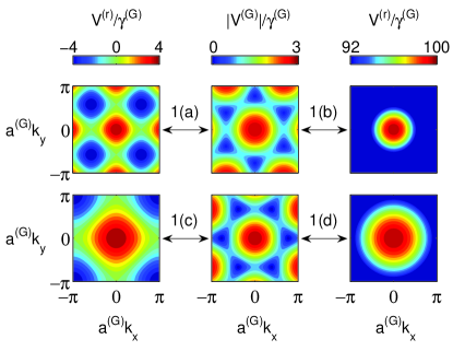
Propagating modes at the Fermi energy can be identified from the condition that the line of constant crosses one of the Fermi lines, which depend on the on-site potential as shown in Fig. 2. This delivers the following conditions for propagating modes on the various types of lattice:
| (8a) | |||
| (8b) | |||
| (8c) | |||
For each type of lattice, these conditions deliver the range of transverse momentum in which the modes are propagating, while in the complementary range the modes are evanescent. The border between these ranges defines the threshold values of transverse momentum at which the modes change their character. In Section IV we translate these thresholds into conductance thresholds for the NGN junctions.
III Numerical results for clean NGN junctions
III.1 Method and parameters
In order to obtain an immediate insight into the gate-voltage dependence of the conductance of the NGN junctions of Fig. 1 we first present numerical results for clean systems.
The transmission coefficients are computed employing an efficient decimation scheme. decimation In this scheme, the uncoupled Hamiltonians of the leads and graphene are reduced to effective Hamiltonians (self-energies) at the interfaces. For square lattice leads the self-energies are known analytically. datta In the graphitic region, the renormalisation procedure is performed iteratively site-by-site employing Gauss-Jordan elimination. The Dyson equation is then used to determine the surface Green function of the coupled system. Finally, the transmission coefficients follow from the Fisher-Lee relation. fisherlee
In our numerical computations, the graphitic region has width and length . In the case of lattice-matched leads, panels (a) and (c) in Fig. 1, the hopping constants in the leads and across the interfaces are all taken to be identical to the hopping constant in graphene, , corresponding to a ballistic interface (without a tunnel barrier). In order to model real-space leads, panels (b) and (d) in Fig. 1, the lattice constant is reduced by a factor as compared to the lattice-matched leads. The hopping constant in the leads is chosen to preserve the effective mass in the parabolic region of the dispersion relation at the bottom of the band. The value for the interface hopping term is again chosen to model a ballistic interface (for a derivation of this value see Appendix B).
III.2 Results
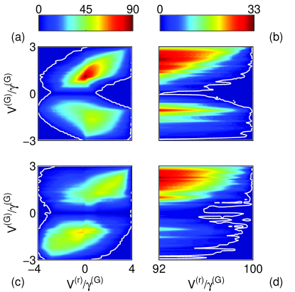
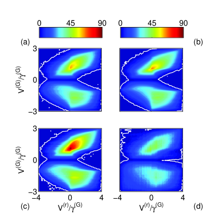
Figures 3(a-d) show the gate voltage dependence of the conductance of clean NGN junctions, where each panel corresponds to one of the configurations in Fig. 1(a-d). The results are presented in a color scale where red corresponds to a large conductance, while blue corresponds to a low conductance. The unit of conductance is the conductance quantum . Regions of low and high conductance are separated by a white contour at . The on-site potential in the graphitic part is varied independently of the on-site potential in the leads. These energies are measured in units of the hopping constant in graphene, . For lattice-matched leads, the on-site potentials are varied over the complete bandwidth of the dispersion relation in the graphitic region () and in the leads (). For real-space leads the on-site potential is restricted to the range in the parabolic region at the bottom of the square-lattice dispersion relation, where is the lattice-constant reduction factor introduced above.
The results in Fig. 3 show a highly systematic dependence of the conductance on the on-site potentials. The conductance is small for , the region of minimal conductivity at zero charge-carrier density discussed in previous transport studies of graphene. Novoselov2005 ; Zhang2005 ; ludwig ; shon ; guinea1 ; tworzydlo ; Nomura ; aleiner ; altland ; ryu ; Ostrovsky ; DasSarma However, we also find regions of very small conductance where the charge-carrier density in graphene and in the leads is finite. Conditions for this insulating behavior are determined in Section IV. The general raggedness of the contours of constant conductance is a common feature in graphene transport studies, and can be associated to Fabry-Perot resonances. guinea2 ; guinea3 ; blanter
For lattice-matched leads with zigzag interfaces [Fig. 3(a)], we observe an approximate mirror symmetry of the conductance for . This symmetry is most pronounced for the regions of low conductance, delimited by the white threshold contour. On the other hand, the maximal conductance for positive is much larger than for negative . These maxima are found at and .
For lattice-matched leads with armchair interfaces [Fig. 3(c)], the mirror symmetry is only observed for the region of low conductance with , close to the top of the square-lattice dispersion relation. The region of high conductance obeys an approximate symmetry when both on-site potentials are inverted, .
For real-space leads [Fig. 3(b, d)], the general features of the conductance are inherited from the behavior for the lattice-matched leads in the parabolic region at the bottom of the square-lattice dispersion relation. In this region, the conductance in general increases for increasing charge-carrier density in the leads (corresponding to smaller values of ), and large values of the conductance are predominantly found for positive . Despite being more ragged, the threshold contours have a similar general trend as in the lattice-matched case. For zigzag interfaces, the region of insulating behavior obeys the approximate mirror symmetry, while this is not the case for armchair interfaces.
IV Analytical results
Most of the conductance thresholds observed in the numerical computations, Fig. 3, can be explained via a simple mechanism, based on the mismatch of propagating modes on both sides of an NG interface. We start our considerations with the exact calculation of the conductance of ballistic NGN junctions with zigzag interfaces and latticed-matched leads [Fig. 1(a)]. The calculation shows that in this case, the insulating regions correspond to conditions where the propagating modes in the normal leads only couple to evanescent modes in the graphitic scattering region. This observation is then carried over as a criterion to calculate conductance thresholds for the other three types of NGN junctions.
IV.1 Conductance for NGN junctions with zigzag interfaces and lattice-matched leads
For ballistic NGN junctions with zigzag interfaces and latticed-matched leads [see Fig. 1(a)] the conductance can be calculated analytically via a wave matching procedure. The calculation succeeds because for the zigzag configuration the hard-wall boundary conditions in the N and G parts select the same transverse wave components, Eqs. (15,16). Hence no mode mixing occurs at a clean zigzag interface. The transmission matrix becomes diagonal, and the wave matching for each fixed transverse-mode profile reduces to a one-dimensional problem.
A derivation of the matching conditions for the present geometry has been given in Refs. schomerus, ; blanter, . The wavefunction in the square leads, , has to be matched with the wavefunction in the graphitic region, at the interfaces of the NGN junction (located at and ), subject to the boundary conditions
| (9) |
In Refs. schomerus, ; blanter, these equations have been solved for the cases , of charge-neutral graphene and for uniformly gated junctions, respectively. For the general case of independent on-site potentials and coupling constants we find
| (10) | |||||
where the dependence of the above expression is implicit in both and , and
| (11) |
The conductance of the junction follows from the Landauer formula (2). In the limit of and one recovers the result of Ref. schomerus, , while for the result of Ref. blanter, is obtained. We confirmed that the values of conductance obtained from Eq. (10) for general combinations of the on-site potentials are in numerical agreement with the results obtained in the previous section [Fig. 3(a)].
IV.2 Conductance thresholds in large ballistic NGN junctions due to mode mismatch
For a long graphitic region, with , a transmission coefficient (10) tends to zero when the propagating mode in the lead couples to an evanescent mode in the graphitic region (i.e., if ). The conductance (2) of the junction is small if this is the case for all transmission coefficients. A small conductance, hence, does not necessitate that all the modes in the graphitic region are evanescent – it suffices that the propagating modes in the graphitic region do not couple to the propagating modes in the leads. Consequently, the conductance can be small even when the charge-carrier density both in the graphitic region as well as in the normal leads is finite. We now apply this mode-mismatch mechanism to calculate conduction thresholds of long and wide ballistic NGN junctions with clean interfaces, covering all of the geometries shown in Fig. 1.
The requirement of a wide junction arises from the fact that the mechanism described above relies on the conservation of transverse momentum (modulo reciprocal-lattice vectors). For a clean zigzag-interface, this conservation law is exact. As discussed in Appendix A, for an armchair interface, the quantized transverse momenta in the graphitic part, Eq. (17), differ from the quantized transverse momenta in the normal leads, Eq. (16). The resulting mode-mixing for interfaces of finite width is discussed in Section V.2. Moreover, details of the transverse-momentum quantization in graphene ribbons depend on the chemistry of the edges. Kawai ; Barone ; Son In wide junctions the modes in N and G are tightly spaced and can be assumed to be quasi-continuous. In the limit , the transverse wave number is then conserved exactly, also for armchair interfaces.
The requirement of a long, ballistic NGN junction is needed so that we can use the assumption that the evanescent modes only give negligible contributions to the conductance, as explained in more detail below. (The effects of disorder are discussed in Section V.)
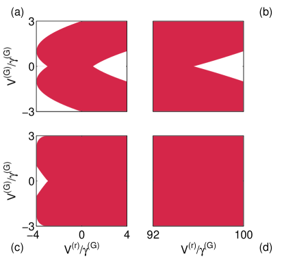
Under these conditions, good conduction requires values of the on-site potentials and at which one finds transverse momenta, possibly differing by reciprocal-lattice vectors, for which the associated modes in N and G are both propagating. The conductance is always small when this criterion is not fulfilled. The threshold values of the on-site potentials separating the regions of matching and mismatching propagating modes can be derived from Eqs. (8).
For the arrangement in Fig. 1 (a), the conductance threshold due to mode mismatch has two branches given by
| (12a) | |||||
| (12b) | |||||
For a finer discretization of the square lattice as in Fig. 1 (b), the first branch remains within the region of the parabolic dispersion at the bottom of the band, while the second branch shifts to . In the continuum limit (5) of the dispersion relation, conductance thresholds due to mode mismatch exist only for , and then are given by
| (13) |
The survival of conductance thresholds in the continuum limit can be best understood by considering the modes with , which propagate in the normal leads for on-site potentials close to the bottom of the parabolic dispersion relation. For zigzag interfaces, these modes propagate in the graphitic region only in the region [see Fig. 2].
For the arrangement in Fig. 1 (c), care has to be taken for the fact that the periods of the Brillouin zones of the leads and the graphene part differ by a factor of in the direction (see the alignment of the Brillouin zones in Fig. 2). The graphitic region hence mediates the coupling of lead modes with different transverse momentum. Propagating modes always match up for , while in the region there are three branches of conductance thresholds due to mode mismatch. Two of these branches are bounded by the condition
| (14a) | |||||
| The third branch is given by the condition | |||||
| (14b) | |||||
For a finer discretization of the square lattice as in Fig. 1 (d), all these branches move to . This results in the absence of conductance thresholds due to mode mismatch in the continuum limit. This can be understood from the observation that in graphene with armchair interfaces, one can find propagating modes with for all values of the on-site potential [see again Fig. 2].
Figure 4 shows the conductance thresholds due to mode mismatch in the – plane. Each panel corresponds to one of the various types of NGN junctions shown in Fig. 1. Comparison with Fig. 3 shows that for zigzag interfaces [panels (a) and (b)], the mode-mismatch mechanism explains all conductance thresholds. For armchair interfaces, the mode-mismatch mechanism explains the conductance thresholds in the left part of panel (c), corresponding to energies close to the top of the band in the leads. The numerical results in Fig. 3(c, d) exhibit additional thresholds in the lower-right corner of the - plane, corresponding to the bottom of the conduction band in the leads and the top of the conduction band in the graphitic part of the system. Here the propagating modes on both sides of the interface differ drastically in their longitudinal wavenumber (and hence in their self-energy), which also inhibits their coupling. schomerus Consequently, the conductance of a ballistic NGN junction can be small even for conditions not described by the simple mode-mismatch mechanism.
IV.3 Sharpness of thresholds
Above we have ignored the contribution of evanescent modes in graphene. These modes become important for a finite system size , and determine the sharpness of the conductance thresholds.
The role of the evanescent modes is best understood by considering the most slowly decaying modes in the graphitic region, and in particular by investigating which of these modes still couple to propagating modes in the leads when one enters the insulating regime. It comes in handy that the most slowly decaying modes have transverse wave numbers just at the threshold to where such modes become propagating, which is determined by Eq. (8). Inside the insulating region, not only all the propagating modes in graphene, but also the adjacent slowly decaying evanescent modes couple to evanescent modes in the leads and hence do not contribute to the transport. The remaining graphitic evanescent modes which do couple to the propagating modes in the leads all have a finite decay constant , and their total contribution to the conductance is suppressed exponentially with . The sharpness of the thresholds hence increases exponentially with the system size.
The decay constant approaches zero as one approaches the conductance thresholds. Let us assume that this is induced by changing the on-site potential at fixed , where depending on the geometry is determined by Eq. (12), (13), or (14). For a vanishing charge-carrier density in graphene, , the linear dispersion relation close to the Dirac point then entails that increases linearly with the distance to the threshold, while for a finite it increases faster, as . Hence, the conductance thresholds are sharper at a finite charge density.
It is insightful to contrast the exponential suppression of the conductance carried by evanescent modes in the insulating region with their contribution inside the conductive region. In this case the most slowly decaying modes do couple to propagating modes in the leads. For a vanishing charge-carrier density in graphene, , the conductance carried by the evanescent modes adds up to a contribution , which is constant and finite at a fixed aspect ratio even when the system is very large. tworzydlo ; schomerus For finite , on the other hand, their contribution is proportional to for and hence decays algebraically for increasing system size. blanter Both expressions require that the most slowly decaying evanescent modes in the graphitic part couple to the propagating modes in the leads, which is not the case in the insulating regime.
V Mode mixing
The derivation of conductance thresholds from the condition of mismatching propagating modes in Section IV relied on the conservation of transverse momentum. In this section we explore how violations of this assumption modify the threshold conditions.
V.1 Mode mixing by disorder
In order to explore the effects of mode mixing by disorder, we implement three different scattering mechanisms: short-ranged bulk disorder and surface roughness in the graphitic region, as well as imperfections at the NG interfaces (long-ranged bulk disorder does not provide efficient mode-mixing). Bulk disorder is modelled via a random on-site potential where the are independently and identically distributed (i.i.d.) random numbers drawn with uniform probability from an interval . For a rough edge we randomly eliminate a fraction of the graphene sites within a distance of from the boundaries of the system. An imperfect interface is modelled via random hopping elements for the links crossing the interface, where the are i.i.d. random numbers drawn with uniform probability from an interval .
Figure 5 presents the results for an NGN junction with zigzag interface and lattice-matched leads [the geometry of Fig. 1(a); the results for the other geometries are similar]. Panel (a) shows the conductance for bulk disorder of strength . Panel (b) shows the conductance for surface roughness with , the value for which we found the strongest effect on the conductance. In both cases, the maximal conductance is reduced to about of the value found in the clean case. This is comparable to what is found in other transport studies at similar levels of disorder. Munoz-Rojas ; guineasurface ; Areshkin ; li ; martinsurface In contrast, the threshold contours delimiting the region of low conductance are only weakly affected by the disorder.
Figure 5(c) shows the conductance for an imperfect interface . This moderate level of imperfection has only a minimal effect on the regions of high and low conductance. A noticeable change of these regions is only induced for a rough interface, shown in Fig. 5(d), where the fluctuations are set equal to the average interface hopping element. At this level of imperfection, the regions of low conductance cover a smaller part in the plane. This has to be attributed to the diffractive effects of a rough interface. It is interesting to observe that the conductance thresholds are most robust around ; especially, the conductance threshold in the region is almost unchanged even though the interface is very rough.
V.2 Mode mixing at clean armchair interfaces
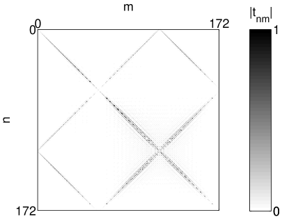
As discussed in Appendix A, the quantized transverse momenta in the graphitic part of an NGN junction with armchair interfaces (and zigzag surface), Eq. (17), differ from the quantized transverse momenta in the normal leads, Eq. (16). This results in a finite amount of mixing even for a clean interface, which is automatically accounted for in the numerical results of Section II. Figure 6 shows a density plot of the modulus of the transmission amplitudes for the NGN junction in Fig. 1(c), with parameters as for the computations in Fig. 3(c). The on-site potentials are set to the values , , where all modes are propagating, so that the mode mixing can be seen in transmission. The figure shows that the transmission matrix is sparse. Each mode mixes with a small number of modes with similar transverse momentum. The additional branches originate from the different periodicity of the Brillouin zones in the leads and the graphitic part, already mentioned in Section IV. At each interface, the transverse momentum is only conserved modulo reciprocal lattice vectors. The periodicity of the Brillouin zone of the leads and the graphitic region in direction differs by a factor of . For the conditions of Fig. 6, this mediates the coupling into two additional branches of transverse momenta in the leads.
VI Conclusions
In this work we systematically investigated the gate-voltage dependence of the conductance of four variants of normal-conductor/graphene/normal-conductor (NGN) junctions, consisting of a graphene strip which is coupled in different ways to normal leads of identical width (c.f. Fig. 1). Starting from exact numerical computations we identified conditions of insulating behavior in clean junctions, which can be encountered even when the charge-carrier density in the central graphitic region and in the normal-conducting leads is finite. Conceptually, this effect can be seen as the counterpart to the celebrated minimal, finite conductivity of graphene close to the charge-neutrality point, where the charge-carrier density nominally vanishes. Novoselov2005 ; Zhang2005 ; ludwig ; shon ; guinea1 ; tworzydlo ; Nomura ; aleiner ; altland ; ryu ; Ostrovsky ; DasSarma
We identified a simple mechanism for the conductance thresholds at finite charge-carrier density, namely the decoupling of the propagating modes in the different parts of the system due to the mismatch of their transverse momenta. Since these momenta are determined by the dispersion relation, the conductance thresholds could in principle be used to obtain information about the band structure of graphene if the dispersion relation in the leads is known. Our numerical computations show that such an analysis would be robust against the effects of bulk and surface disorder in the graphitic region, and would also tolerate a moderate amount of imperfection of the interfaces.
Acknowledgements.
We gratefully acknowledge helpful discussions with Vladimir Fal’ko and Edward McCann, as well as useful correspondence with Andre Geim and Philip Kim. This work was supported by the European Commission, Marie Curie Excellence Grant MEXT-CT-2005-023778.Appendix A Transverse-momentum quantization
In a wire geometry, the boundary conditions select a discrete set of transverse wave numbers for a given propagation or decay direction, which we enumerate by a mode index . The details of the transverse-momentum quantization of graphene ribbons depend on the chemistry of the edges. Kawai ; Barone ; Son In this paper, we are mostly concerned with wide graphitic regions, where the transverse momentum becomes quasi-continuous. When we, in the following, give expressions for in the tight-binding model used in the numerical simulations, it should be noted that the dimension refers to the width of the interface, which is identical to the width of the square-lattice leads but differs from the width of the graphitic region (which is wider by for zigzag interfaces and by for armchair interfaces).
On the square lattice, is the number of sites in the cross-section of the wire, and the set of quantized transverse wave numbers is given by
| (15) |
On the hexagonal lattice with zigzag interfaces (and hence armchair boundaries), , and the set of quantized transverse wave numbers is given by
| (16) |
Both sets of quantized transverse wave numbers become identical when the lattices are matched commensurably as shown in Fig. 1(a), where .
More complicated is the case of the hexagonal lattice with armchair interface (which has zigzag edges), shown in Fig. 1(b). At the upper (lower) edge, hard-wall boundary conditions translate into a vanishing amplitude on the A (B) sites in the first unit cell beyond the wire boundary. Since the amplitudes on these sites carry a relative phase which depends on the propagation direction, the quantized transverse wave numbers are determined by a transcendental equation,
| (17) |
For and close to the K points, this equation reduces to the condition derived from the Dirac equation given in Ref. brey, . In general, Eq. (17) has independent solutions. For , this includes a number of edge states with . For wide interfaces (), the real-valued transverse wave numbers are almost uniformly spaced, but do not coincide with the transverse wave numbers of the lattice-matched square lattice with , shown in Fig. 1(b).
Appendix B Interface hopping constant for a transparent interface with a real-space lattice
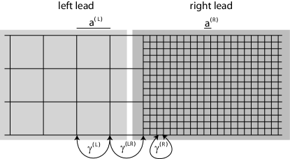
In this appendix we describe how to model a transparent interface between a tight-binding lattice and a real-space lattice, as shown in Fig. 1(b,d). A simpler variant of such an interface, well suited for analytical calculations, is the interface of two commensurably matched square-lattice leads with different lattice constant, shown in Fig. 7. The lattice constants in the left and right lead are related by an integer-valued reduction constant so that ; the continuum limit of the right lead is approached for . This simple arrangement is representative for couplings of real space leads to other tight-binding lattices, since only the sites adjacent to the interface enter the subsequent considerations.
The hopping constants in the left and right lead are denoted by and , respectively. In our numerical computations we further made the assumption that these constants are related by the requirement of an identical effective mass . The hopping constants in the two leads are then related by .
Our goal is to determine the inter-lead hopping constant, , so that the lead is transparent for energies in the parabolic region of the dispersion relation at the bottom of the bands of both leads.
We choose a coordinate system where the right lead starts at and the origin accommodates one of the lattice sites that is linked to the left lead. Now consider a particle arriving from the left lead at a fixed energy and transverse wave number , which are both conserved under reflection from the interface. The wave function
| (18) |
then describes the superposition of the incoming and reflected particle, where the longitudinal wave number is fixed by the dispersion relation (4).
Upon crossing the interface, the transverse momentum is conserved modulo reciprocal lattice vectors. Since the Brillouin zone in the right lead is larger by a factor , one couples into inequivalent modes with wavenumber , . For energies close to the bottom of the bands in both leads, only the mode with is propagating while the others are evanescent. We denote the longitudinal wavenumber of the propagating mode by , and the decay constant of the evanescent modes by , . The wave function in the right lead is hence given by
| (19) |
The relative amplitudes of the evanescent modes are fixed by the boundary condition on those sites at which have no link to left lead. Since the wavefunction (19) would fulfil the Schrödinger equation when the right lead would be continued beyond the interface, this boundary condition can be formally expressed as , where , with , is the transverse coordinate of inequivalent disconnected sites. These boundary conditions are fulfilled when the amplitudes take the value .
The remaining amplitudes , , and are now obtained from the boundary conditions of the sites on both leads which are linked to the other lead. Using again the fact that the wavefunctions (18) and (19) both fulfil the Schrödinger equation when the leads would be extended across the interface, these conditions can be written as
| (20) | |||
| (21) |
The reflection amplitude then follows as
| (22) |
where
| (23) |
At the bottom of the band, we can further assume , and the decay constants approach the value . The condition for a transparent interface then gives the desired expression for the coupling constant, which after some algebraic manipulations can be written as
| (24) | |||
The value used in the numerical computations finally follows when Eq. (24) is evaluated for and a lattice-constant reduction factor .
References
- (1) K. S. Novoselov, A. K. Geim, S. V. Morozov, D. Jiang, Y. Zhang, S. V. Dubonos, I. V. Grigorieva, and A. A. Firsov, Science 306, 666 (2004).
- (2) A. K. Geim and K. S. Novoselov, Nature Materials 6, 183 (2007).
- (3) R. Saito, G. Dresselhaus, M. Dresselhaus, Physical Properties of Carbon Nanotubes (Imperial College Press, London, 1998).
- (4) D. P. DiVincenzo and E. J. Mele, Phys. Rev. B 29, 1685 (1984).
- (5) K. S. Novoselov, A. K. Geim, S. V. Morozov, D. Jiang, M. I. Katsnelson, I. V. Grigorieva, S. V. Dubonos, and A. A. Firsov, Nature 438, 197 (2005).
- (6) K. S. Novoselov, E. McCann, S. V. Morozov, V. I. Fal’ko, M. I. Katsnelson, U. Zeitler, D. Jiang, F. Schedin, and A. K. Geim, Nature Phys. 2, 177 (2006).
- (7) Y. Zhang, J. W. Tan, H. L. Stormer, and P. Kim, Nature 438, 201 (2005).
- (8) K. S. Novoselov, Z. Jiang, Y. Zhang, S. V. Morozov, H. L. Stormer, U. Zeitler, J. C. Maan, G. S. Boebinger, P. Kim, and A. K. Geim, Science 315, 1379 (2007).
- (9) A. W. W. Ludwig, M. P. A. Fisher, R. Shankar, and G. Grinstein, Phys. Rev. B 50, 7526 (1994).
- (10) S. Ryu, C. Mudry, A. Furusaki, and A. W. W. Ludwig, Phys. Rev. B 75, 205344 (2007).
- (11) N. H. Shon and T. Ando, J. Phys. Soc. Jpn. 67, 2421 (1998).
- (12) N. M. R. Peres, F. Guinea, and A. H. Castro Neto, Phys. Rev. B 73, 125411 (2006).
- (13) J. Tworzydło, B. Trauzettel, M. Titov, A. Rycerz, and C. W. J. Beenakker, Phys. Rev. Lett. 96, 246802 (2006).
- (14) K. Nomura and A. H. MacDonald, Phys. Rev. Lett. 98, 076602 (2007).
- (15) I. L. Aleiner and K. B. Efetov, Phys. Rev. Lett. 97, 236801 (2006).
- (16) A. Altland, Phys. Rev. Lett. 97, 236802 (2006).
- (17) P. M. Ostrovsky, I. V. Gornyi, and A. D. Mirlin, Phys. Rev. B 74, 235443 (2006); Phys. Rev. Lett. 98, 256801 (2007).
- (18) S. Adam, E. H. Hwang, V. M. Galitski, and S. Das Sarma, arXiv:0705.1540 (2007).
- (19) S. V. Morozov, K. S. Novoselov, M. I. Katsnelson, F. Schedin, L. A. Ponomarenko, D. Jiang, and A. K. Geim, Phys. Rev. Lett. 97, 016801 (2006).
- (20) X. Wu, X. Li, Z. Song, C. Berger, and W. A. de Heer, Phys. Rev. Lett. 98, 136801 (2007).
- (21) R. V. Gorbachev, F. V. Tikhonenko, A. S. Mayorov, D. W. Horsell, and A. K. Savchenko, Phys. Rev. Lett. 98, 176805 (2007).
- (22) E. McCann, K. Kechedzhi, V. I. Fal’ko, H. Suzuura, T. Ando, and B. L. Altshuler, Phys. Rev. Lett. 97, 146805 (2006).
- (23) A. F. Morpurgo and F. Guinea, Phys. Rev. Lett. 97, 196804 (2006).
- (24) K. Kechedzhi, V. I. Fal’ko, E. McCann, and B. L. Altshuler, Phys. Rev. Lett. 98, 176806 (2007).
- (25) T. Ohta, A. Bostwick, T. Seyller, K. Horn, and E. Rotenberg, Science 313, 951 (2006); A. Bostwick, T. Ohta, T. Seyller, K. Horn, and E. Rotenberg, Nature Physics, 3, 36 (2007); T. Ohta, A. Bostwick, J. L. McChesney, T. Seyller, K. Horn, and E. Rotenberg, Phys. Rev. Lett. 98, 206802 (2007).
- (26) S. Y. Zhou, G. H. Gweon, C. D. Spataru, J. Graf, D. H. Lee, S. G. Louie, and A. Lanzara, Phys. Rev. B 71, 161403(R) (2005); S. Y. Zhou, G.-H. Gweon, J. Graf, A. V. Fedorov, C. D. Spataru, R. D. Diehl, Y. Kopelevich, D.-H. Lee, S. G. Louie, and A. Lanzara, Nature Physics 2, 595 (2006).
- (27) V. V. Cheianov, V. Fal’ko, and B. L. Altshuler, Science 315, 1252 (2007).
- (28) A. Rycerz, J. Tworzydło, and C. W. J. Beenakker, Nature Physics 3, 172 (2007).
- (29) M. Fujita, K. Wakabayashi, K. Nakada, and K. Kusakabe, J. Phys. Soc. Japan 65, 1920 (1996).
- (30) K. Nakada, M. Fujita, G. Dresselhaus, and M. S. Dresselhaus, Phys. Rev. B 54, 17954 (1996).
- (31) K. Wakabayashi, M. Fujita, H. Ajiki, and M. Sigrist, Phys. Rev. B 59, 8271 (1999).
- (32) Y. Miyamoto, K. Nakada, and M. Fujita, Phys. Rev. B 59, 9858 (1999).
- (33) L. Brey and H. A. Fertig, Phys. Rev. B 73, 235411 (2006).
- (34) M. Ezawa, Phys. Rev. B 73, 045432 (2006);
- (35) K.-I. Sasaki, S. Murakami, and R. Saito, J. Phys. Soc. Jpn. 75, 074713 (2006).
- (36) N. M. R. Peres, A. H. Castro Neto, and F. Guinea, Phys. Rev. B 73, 195411 (2006).
- (37) E. Prada, P. San-Jose, B. Wunsch, and F. Guinea, Phys. Rev. B 75, 113407 (2007).
- (38) B. Huard, J.A. Sulpizio, N. Stander, K. Todd, B. Yang, and D. Goldhaber-Gordon, Phys. Rev. Lett. 98, 236803 (2007).
- (39) H. Schomerus, Phys. Rev. B 76, 045433 (2007).
- (40) Y. M. Blanter and I. Martin, arXiv:cond-mat/0612577 (2006).
- (41) M. Y. Han, B. Özyilmaz, Y. Zhang, P. Kim, Phys. Rev. Lett 98, 206805 (2007).
- (42) M. A. Topinka, R. M. Westervelt, and E. J. Heller, Physics Today 56 (12), 47 (2003).
- (43) An introduction to this decimation algorithm can be found in H. M. Pastawski and E. Medina, Rev. Mex. Phys. 47, 1 (2001) [arXiv:cond-mat/0103219].
- (44) S. Datta, Electronic Transport in Mesoscopic Systems (Cambridge University Press, Cambridge, 1997).
- (45) D. S. Fisher and P. A. Lee, Phys. Rev. B 23, 6851 (1981).
- (46) T. Kawai, Y. Miyamoto, O. Sugino, Y. Koga, Phys. Rev. B 62, R16349 (2000).
- (47) V. Barone, O. Hod, and G. E. Scuseria, Nano Lett. 6, 2748 (2006).
- (48) Y.-W. Son, M. L. Cohen, and S. G. Louie, Phys. Rev. Lett. 97, 216803 (2006).
- (49) F. Muñoz-Rojas, D. Jacob, J. Fernández-Rossier, and J. J. Palacios, Phys. Rev. B 74, 195417 (2006).
- (50) E. Louis, J. A. Vergés, F. Guinea, and G. Chiappe, Phys. Rev. B 75, 085440 (2007).
- (51) D. A. Areshkin, D. Gunlycke, C. T. White, Nano Lett. 7, 204 (2007).
- (52) T. C. Li, S.-P. Lu, arXiv:cond-mat/0609009 (2006).
- (53) I. Martin and Ya. M. Blanter, arXiv:0705.0532 (2007).