Polaronic state and nanometer-scale phase separation in colossal magnetoresistive manganites
Abstract
High resolution topographic images obtained by scanning tunneling microscope in the insulating state of Pr0.68Pb0.32MnO3 single crystals showed regular stripe-like or zigzag patterns on a width scale of 0.4–0.5 nm confirming a high temperature polaronic state. Spectroscopic studies revealed inhomogeneous maps of zero-bias conductance with small patches of metallic clusters on length scale of 2–3 nm only within a narrow temperature range close to the metal-insulator transition. The results give a direct observation of polarons in the insulating state, phase separation of nanometer-scale metallic clusters in the paramagnetic metallic state, and a homogeneous ferromagnetic state.
pacs:
71.30.+h, 75.47.Lx, 68.37.EfThere is an intense research going on to understand the remarkable and complex properties shown by a whole family of strongly correlated electron systems. In these materials, a self-inflicted, spontaneous instability of the electronic state and competing long-range interactions may result in the formation of nanometer-sized regions of different phases. Such states have been considered as charge and spin ordered stripes in under-doped cuprates kiv , as polar domains in relaxor ferroelectrics find , or as phase separation (PS) between insulating paramagnetic (pm) and conducting ferromagnetic regions dag in mixed valence manganites of perovskite type MnO3 (–rare earth or doped divalent ion). In the latter case, evidence for PS has been found by various experimental techniques, such as electron microscopy ueh , scanning tunneling microscopy/spectroscopy (STM/S) fat ; bec , magnetic force microscopy zha and photoelectron spectroscopy sar . These experiments showed inhomogeneities of random shape on a length scale of several hundred nanometers. Further, the PS persisted deep into the metallic state in some of these manganites. However, computational studies on models of manganites considering double exchange, Jahn-Teller (JT) interaction and long range Coulomb potential could show only regularly spaced nanometer-scale PS mal . The random location and shape of the clusters observed experimentally ueh ; fat ; bec ; zha ; sar are conjectured to be caused by quenched disorder in the couplings induced by chemical substitution mo1 ; mo2 . Recent STS studies combined with transmission electron microscopy mos on -site ordered and disordered La0.75Ca0.25MnO3 thin films showed that PS persists in the metallic state only in the disordered film. But, this study does not address the question of PS at the metal-insulator transition temperature, . Thus, the origin of the PS, the length scale involved, the role of quenched disorder originating from the random -site substitution, and the temperature range at which PS occurs, remain all strongly debated.
The polaron effect due to strong JT electron-phonon coupling is considered central to understand the remarkable transport properties, specifically the colossal magnetoresistance (CMR), of manganites mil . The high temperature polaronic state in reciprocal space has been probed experimentally vas ; nel revealing complex polaron effects such as polaron correlation, polaron ordering, and charge localization. Using STM, polarons can be imaged directly in the real space. Polaron confinement was recently observed in a layered manganite single crystal using STM ron . Charge ordering was reported for thin films (La5/8-xPrx)Ca3/8MnO3 [short range charge exchange (CE) type] in the pm state ma and for highly doped Bi0.24Ca0.76MnO3 single crystals ren-nat .
Spatially resolved STS measurements fat on thin films of La0.73Ca0.27MnO3 on SrTiO3 showed coexistence of regions with metallic, insulating as well as intermediate conductivities, extending over several hundred nanometers. However, these images were obtained at a rather high fixed bias voltage of 3 V (much larger than the semiconducting gap of 0.2–0.3 V in manganites) and may not reflect the ground state properties. On the other hand, in Ref. bec, the zero-bias conductance, , of La0.7Sr0.3MnO3/MgO thin films was mapped as a function of temperature , and a threshold criterion was applied to distinguish metallic and insulating regions. Such a threshold criterion will not give an unambiguous evidence for the existence of PS because any statistical distribution of conductance, whose average value shifts with , will seem to show PS ren . Further, in thin film samples, miss-fit strain induced by the substrates seems to influence the electrical properties par .
To resolve some of these issues from experimental side, we carried out STM/S on Pr0.68Pb0.32MnO3 (PPMO) single crystals providing largely strain-free materials. We address two important questions in the physics of manganites, namely, the high temperature polaronic state and the nanometer-scale electronic PS. We present STM images of polaronic Mn3+-sites and doped hole localization on Mn4+-sites with atomic resolution. In addition, we provide clear evidence for nanometer-scale PS and percolation just below by looking at the entire distribution of and its dependence on . Information on the length scale of the inhomogeneities and the range within which it appears is obtained. We discuss the role of quenched disorder or doping and compare the results with macroscopic properties of the same single crystal.
Single crystals of PPMO used for the present study were taken from a batch of crystals, whose preparation and properties were already

reported in pa1 ; pa2 . In Pr1-xPbxMnO3, the Curie temperature and do not coincide, and metal-like conductivity occurs in a pm state in parts of the phase diagram pa1 ; li , a phenomenon uncommon to mixed valence manganites. Fig. 1 shows the temperature dependence of magnetization (), resistivity () and magnetoresistive properties of a PPMO sample. The magnetoresistance, , is found to be 90% close to under a field of 9 T. From the maximum change in slope of the vs. curve, 210 K was estimated which is about 45 K lower than the corresponding 255 K. Such an approach to estimate is supported by elaborate investigations on a similar Pr0.7Pb0.3MnO3 single crystal in which the so-determined 197 K agrees well with results from detailed static magnetization scaling analysis pa2 as well as heat capacity measurements pa3 ( 235 K in this compound pa1 ). The scaling analysis embracing the critical temperature indicated that the underlying magnetic transition is a conventional one, with short-range Heisenberg-like critical exponents. This study emphasizes on the presence of additional frustrated couplings which intercepts the formation of long range order. Deviation of the inverse susceptibility from the Curie-Weiss law above pa1 and history-dependent transport properties li suggest a
presence of small magnetic metallic clusters above that form percolating metallic paths upon reducing in the pm metallic state. Note that evidence for the formation of localized 1.2 nm magnetic clusters above in another mixed valent manganite has earlier been found by small-angle neutron scattering measurements det . We also note the sharpness of the resistance transition which can be inferred from the logarithmic derivative of the resistance plotted in the inset of Fig. 1. Such a sharp metal-insulator transition is indicative of a strain-free sample par (the tolerance factor, 0.965, is close to unity indicating good ionic size match).
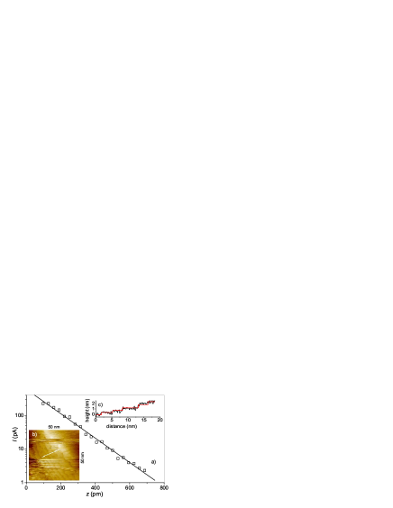
For the tunneling studies a STM (Omicron Nanotechnology) under ultra high vacuum conditions ( mbar) was utilized at eleven fixed temperatures, 30 K 300 K, mostly in the vicinity of and . Since crystals with perovskite structure do not cleave easily, preparation of a clean surface for the STM is a challenge. Just before inserting the crystal into the UHV chamber, we thoroughly cleaned the crystal surface in isopropanol using an ultrasonic bath and then, inside isopropanol, scraped the surface to rip off some part of the surface. This preparation gave us clean surfaces on a length scale of microns. STM was conducted using tungsten tips, and typically 0.3 nA for the current set point and 0.8 V for the bias voltage, . This implies that we probed the unoccupied electronic DOS of PPMO. Fig. 2(a) shows the dependence of tunneling current on relative tip-sample distance on a semi-logarithmic plot. The exponential nature of confirms an excellent vacuum tunnel barrier (effective work function 1.5 eV). Topography (50 50 nm2) is presented in inset (b). Terraces with unit cell height (0.4 nm) steps [Fig. 2, inset (c)] indicate surface of the pseudocubic perovskite crystal.
High resolution STM images taken in the insulating regime (at 300 K) on the terraces indicate bright and dark regions forming stripe-like features spread over a length scale of 0.4–0.5 nm, as seen in Fig. 3(a), (b). While probing the unoccupied electronic DOS the doped holes localized on Mn4+ sites appear as bright spots in the STM image, whereas electron tunneling from a conventional metallic tip into a polaronic state
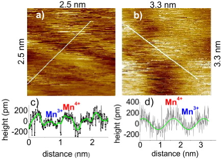
(e.g. electrons localized on Mn3+ ions) is difficult and produces dark spots ma . However, these contrasts were seen only occasionally, an observation similar to what was reported in the case of layered manganite La2-2xSr1+2xMn2O7 ron . This suggests the short-range stripe-like order of Mn3+ and Mn4+ ions. The extent of these features [Fig. 3(c) and (d)] is slightly larger than the typical atomic distance of 0.39 nm in the cubic perovskite cell and comparable with charge ordered stripes observed in high resolution lattice images of La0.33Ca0.67MnO3 mor . Short-range polaron correlation and CE-type of charge ordering was observed in manganites using diffused x-ray and neutron scattering vas ; nel . Recent STM studies ma probing simultaneously the occupied and unoccupied states of (La5/8-xPrx)Ca3/8MnO3 thin films also showed short-range CE-type charge ordered clusters in the pm state.
To map the surface electronic state, we carried out thousands of STS measurements at different locations on the sample
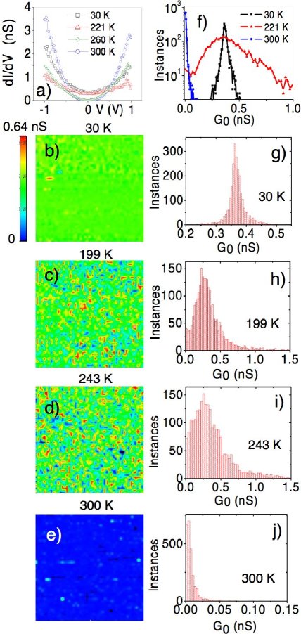
surface spanning the range from 28 – 300 K. Typically, a surface area of 50 50 nm2 with a lateral resolution of 1 nm (2500 pixels) was investigated. Tunneling current and differential conductance, , were measured simultaneously while ramping from to +1 V. An average of 2500 - curves taken at representative 30, 221, 260 and 300 K are shown in Fig. 4(a). At 30 K, the - curve is metal-like with a finite value of signifying a finite DOS at the Fermi energy. In contrast, at 300 K, i.e. 255 K, the - curve around 0 is typical of a semiconducting gap. In the pm metallic state at 221 K, the value of is only slightly reduced compared to K, thus showing an expected dependence of the conductance.
For quantifying the STS results and mapping the homogeneity of the DOS laterally as well as its temperature evolution, we plot as conductance maps at selected . In Fig. 4(b)–(e), the local is presented color-coded (with a color scale covering 0 0.64 nS) at 30, 199, 243 and 300 K, respectively. Corresponding distributions for the frequency of the observed values are shown in the histograms Fig. 4(g)–(j). A sharp distribution of at 30 K confirms a homogeneous electronic phase at low temperature. Similarly, the conductance map at 300 K (in the semiconducting region) is also homogeneous [Fig. 4(e)], with most of the values of very close to zero [Fig. 4(j)].
On the other hand, as is raised through and approaches 255 K inhomogeneities start to develop at a length scale of 2 – 3 nm, as seen in Fig. 4(c) and (d). The peak in the histograms [panels (h), (i)] shifts to lower conductance values as is increased and, importantly, an increasing weight at 0 is observed. A bimodal distribution of at 221 K is clearly visible in Fig. 4(f), with two maxima in frequency located at similar values as for low and high , respectively. The distributions near [cf. Fig. 4(f)] are significantly broadened compared to both, low (30 K) and high 300 K . The sharp distribution at 300 K clearly indicates that these broad distributions of at intermediate reflect a sample property rather than an instrumental influence.
The dependences observed in STS arise not only from the Fermi function, but also the sample’s DOS itself is dependent. This change of electronic properties can be explained by the release of lattice distortions around , when the immobilized polaronic carriers become successively mobile producing inhomogeneous spatial conductance distributions and electronic transport through percolating metallic regions. Thus, the increasing weight at 0 while retaining a peak at 0.3 nS provides a direct observation of nanometer-scale PS in PPMO single crystals. Interestingly, this PS appears to be restricted to the transition region in this compound. The drastic change in and its distribution with at around the bulk indicates that our STS results are not mere surface effects.
Our results are distinct from previous experimental results where PS is seen on a micrometer scale and persisted well within the metallic regime. It remains an open question, whether the particular properties of PPMO with a metallic pm state in the region are responsible for the clear observation of this nanometer-scale PS phenomenon and whether the result can be generalized to other mixed-valence manganites (as pointed out before the electrical transport in PPMO occurs via percolation of nanometer-scale metallic clusters for ). Further, the specific pattern of electronic inhomogeneitiy in the local surface DOS is certainly affected by disorder, induced by random chemical substitutions and/or surface effects. In addition, disorder effects due to size differences between -site Pr3+ and Pb2+ ions may play a role. However, the observed nanometer-scale PS is not a simple and fixed result of static chemical disorder, as can be inferred from the homogeneity of the electronic properties deep in the metallic state (low ) as well as in the insulating one (300 K). Hence, in order to resolve the relevance of disorder effects on PS and the associated length scale, similar spatially resolved STS studies on different manganites are called for.
In summary, our high resolution STM images provide direct evidence for the high temperature polaronic state in perovskite manganite. Polarons are confined to one lattice cell. Stripe-like features seen occasionally in these images suggest a short-range ordering of these polarons in the form of a lattice. Spatially resolved STS images show nanometer-scale phase separation in the paramagnetic metallic state. However, the homogeneous low- as well as high temperature STS images confirm that this phase separation is limited only to the temperatures close to the metal-insulator transition suggesting that it is related to the non-coincidence of and .
We are grateful to U. K. Rößler, Ch. Renner and G. Aeppli for valuable discussions. We acknowledge financial support by the DFG, grant WI 1324/1-1, and the European Commission through CoMePhS 517039.
References
- (1) S. A. Kivelson et al., Rev. Mod. Phys. 75, 1201 (2003).
- (2) W. Eerenstein, N. D. Mathur, and J. F. Scott, Nature (London) 442, 759 (2006).
- (3) E. Dagotto “Nanoscale phase separation and colossal magnetoresistance” (Spinger, Heidelberg, 2002).
- (4) M. Uehara, S. Mori, C. H. Chen, and S.-W. Cheong, Nature (London) 399, 560 (1999).
- (5) M. Fäth, S. Freisem, A. A. Menovsky, Y. Tomioka, J. Aarts, and J. A. Mydosh, Science 285, 1540 (1999).
- (6) T. Becker et al., Phys. Rev. Lett. 89, 237203 (2002).
- (7) L. Zhang, C. Israel, A. Biswas, R. L. Greene, and A. de Lozanne, Science 298, 805 (2002).
- (8) D. D. Sarma et al., Phys. Rev. Lett. 93, 097202 (2004).
- (9) A. L. Malvezzi, S. Yunoki, and E. Dagotto, Phys. Rev. B 59, 7033 (1999).
- (10) A. Moreo, S. Yunoki, and E. Dagotto, Science 283, 2034 (1999).
- (11) A. Moreo et al., Phys. Rev. Lett. 84, 5568 (2000).
- (12) V. Moshnyaga et al., Phys. Rev. Lett. 97, 107205 (2006).
- (13) A. J. Millis, P. B. Littlewood, and B. I. Shraiman, Phys. Rev. Lett. 74, 5144 (1995).
- (14) L. Vasiliu-Doloc et al., Phys. Rev. Lett. 83, 4393 (1999).
- (15) C. S. Nelson et al., Phys. Rev. B 64, 174405 (2001).
- (16) H. M. Rønnow, Ch. Renner, G. Aeppli, T. Kimura, and Y. Tokura, Nature (London) 440, 1025 (2006).
- (17) J. X. Ma, D. T. Gillaspie, E. W. Plummer, and J. Shen, Phys. Rev. Lett. 95, 237210 (2005).
- (18) Ch. Renner, G. Aeppli, B.-G. Kim, Y.-A. Soh, and S.-W. Cheong, Nature (London) 416, 518 (2002).
- (19) Ch. Renner and H. M. Rønnow, in Scanning Probe Microscopy: Electrical and Electromechanical Phenomena at the Nanoscale, ed. S. Kalinin (Spinger, Berlin, 2006).
- (20) M. Paranjape, A. K. Raychaudhuri, N. D. Mathur, and M. G. Blamire, Phys. Rev. B 67, 214415 (2003).
- (21) B. Padmanabhan et al., J. Magn. Magn. Mater. 307, 288 (2006).
- (22) B. Padmanabhan et al., Phys. Rev. B 75, 024419 (2007).
- (23) R.-W. Li, X. Zhou, B.-G. Shen, and B. Hillebrands, Phys. Rev. B 71, 092407 (2005).
- (24) B. Padmanabhan, unpublished.
- (25) J. M. DeTeresa et al., Nature (London) 386, 256 (1997).
- (26) S. Mori, C. H. Chen, and S. W. Cheong, Nature (London) 392, 473 (1998).