Localized Electron States Near a Metal-Semiconductor Nanocontact
Abstract
The electronic structure of nanowires in contact with metallic electrodes of experimentally relevant sizes is calculated by incorporating the electrostatic polarization potential into the atomistic single particle Schrödinger equation. We show that the presence of an electrode produces localized electron/hole states near the electrode, a phenomenon only exhibited in nanostructures and overlooked in the past. This phenomenon will have profound implications on electron transport in such nanosystems. We calculate several electrode/nanowire geometries, with varying contact depths and nanowire radii. We demonstrate the change in the band gap of up to 0.5 eV in 3 nm diameter CdSe nanowires and calculate the magnitude of the applied electric field necessary to overcome the localization.
pacs:
73.22.-f,73.40.Ns,73.43.CdFurture nanoelectronics will depend on electron/hole transport in a nanostructure, and crossing the nanostructure/metal electrode interface. Understanding the properties of such nanocontacts, especially new phenomena unique to the nanocontacts is thus of paramount importance to the future of nanoelectronics and it is currently an intensively studied subject. Significant progress has been made in recent years in fabricating variety of nanostructures and nanocontacts ranging from 0D structures like isolated quantum dots, to more sophisticated structures, such as tetrapods, nanoribbons, nanorods and nanowires, etc. Manna et al. (2003); Milliron et al. (2004); Gao and Wang (2002). Transport measurements in such nanostructures are often conducted by contacting a semiconductor nanostructure with large metallic electrodes, often deposited on top of the nanostructure.Klein et al. (1997); Fang et al. (2007); Steiner et al. (2005); Heo et al. (2004); Cui et al. (2005); Thelander (2003); Zhang et al. (1999); Gudiksen et al. (2002) Hitherto, theoretical interpretation of such experiments has often been based on transport and electronic structure calculations with isolated nanostructures and ignoring influence of the electrodes. Even if the electrode is included in the calculation, its effects are often described by a short range correlation theory, such as local density approximation (LDA). For example, a nanocontact between an extremely small Si nanowire (with a diameter of 5 Å) and Al electrode has been calculated by U. Landman et al. Landman et al. (2004). However, due to the use of LDA, the authors did not find the localization effects shown in this letter. The existence of the electrode will introduce the long range correlation effects well into the semiconductor nanowire, causing the change of its electronic structure. The long range correlation effects cannot be described by LDA, they can only be addressed by many-body theories, like the method, albeit the high cost of the method prevents it from being used to calculate the systems we discuss here. Fortunately, in the static approximation, the long range correlation effect allows a simple classical interpretation. Wang (2005) It can be represented by an additional potential in the single particle Schrödinger equation, corresponding to a classical surface polarization potential (or image potential for metal). As we show below, this surface polarization potential is surprisingly large, particularly for small nanostructures, where it alters the familiar electronic structure and gives rise to a nanocontact phenomenon: electrode induced wavefunction localization. This localization disappears when the system becomes large, which explains why it has been overlooked in the past.
In this letter we study the common case of the CdSe nanowire attached to a generic metallic contact. In practical calculations we use a long nanorod to represent a nanowire. The physical properties of CdSe nanorods such as optical spectroscopy, conductivity, electric dipole, etc., have been extensively studied in the past decade Katz et al. (2002); Li and Alivisatos (2003); LeThomas et al. (2005); Krishnan et al. (2004) both experimentally and theoretically. The charging properties of isolated nanostructures (which are dependent on the surface polarization potential) have been studied theoretically, for quantum dots Franceschetti and Zunger (2000); Rabani et al. (1999); Stopa (1996); Fonoberov et al. (2002), and tetrapods Wang (2005). It has been demonstrated that the surface polarization potential (when the set up does not include a metallic electrode) plays an important part in the quantum dot charging energy.Wang (2005) Here we study the electronic properties of the CdSe nanorods in contact with metallic electrodes taking into account surface polarization potential. We use semi-empirical pseudopotential method (SEPM) to describe electron Schrödinger equation Wang and Zunger (1996). We assume that the metal electrode makes a Schottky contact with semiconductor nanorod as suggested in Ref. Léonard and Talin, 2006 (to avoid possible complications due to charge transfer).
Within the SEPM we ordinarily solve the single-particle Schrödinger equation using planewave basis sets
| (1) |
where, is a potential which includes both local (sum of the screened atomic pseudopotentials) and nonlocal (, and spin-orbit coupling) parts. The pseudopotentials are fitted to match the bulk experimental band structure. The potential is bulk-like inside and zero outside the nanorod. The dangling bonds at the nanorod surface are passivated with a model ligand potentials to eliminate the midgap surface states. Once the potential for the entire nanorod is constructed, the Eq. 1 can be used to solve for the eigenenergies and the wavefunctions in the nanorod. In practice, we use the folded-spectrum method (FSM) Wang and Zunger (1994) in order to solve for only a few states in the valence and conduction band adjacent to the bandgap. The use of FSM allows us to perform calculations of large nanostructures containing tens of thousands of atoms, and approach experimentally relevant sizes range.
In the presence of the electrode, the surface polarization potential due to interaction of an electron with its image charge becomes significant. Proper treatment of these long range correlations requires a many-body approach, such as method. However, it has been shown Wang (2005) that (under a static approximation) the self-energy potential in equation can be split into a bulk potential and a surface polarization potential. The equation is then split into two parts, the bulk Hamiltonian (analogous to Eq.1) and the surface polarization part, which is reduced to an electrostatic surface polarization potential . Thus, the equation can be approximated as
| (2) |
where + and - are applied to electron and hole states, respectively, and are the quasiparticle energies. In the nanostructure the polarization potential can be derived from the many-body model, Wang (2005) which results in the same form as in the early electrostatic model of Brus Brus (1983, 1984)
| (3) |
where is the screened electrostatic potential in the nanorod at created by a test charge at , and is such potential in the bulk. In order to find the electrostatic potential we solve the Poisson equation for the structure shown in the inset to Fig.1 (electrode size not to scale)
| (4) |
. The dielectric function is modeled following our study of dielectric response of a nanostructure Cartoixa and Wang (2005), which equals at the center of the nanorod, and approaches 1 near the surface of the rod. We use Dirichlet boundary conditions of at the domain boundary and and obtain which is then added to the previously computed CdSe nanorod potential in the Eq. 2, for the subsequent SEPM calculation of the electronic structure.
We calculated surface polarization potential for nanorods length of 23 nm, and the diameters of 1.5, 3, 6, and 10 nm. The diameter of the electrode was much larger than that of the nanorod (=23 nm) in order to minimize the influence of a specific electrode geometry and mimic the situation of many experimental nanocontact setups. The SEPM calculations were performed for CdSe nanorods in the wurtzite crystal structure, length of 23 nm, and 3 nm diameter, with total number of atoms of 5434. The polarization potential was generated for a) the nanorods embedded into a metal electrode by one half and one quarter of its length, b) nanorod and the electrode in contact, c) nanorod and the electrode separated by a 1 nm layer of vacuum, and d) a free standing nanorod.
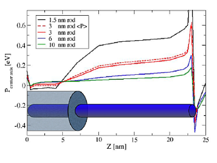
Figure 1 shows the polarization function as a function of the -coordinate running along the nanorod central axis, for nanorod diameter ranging from 1.5 to 10 nm, in the case of the nanorod embedded into the electrode by a quarter of its length. For the 3 nm rod we also computed the weighted average as
| (5) |
where , and is taken either as a conduction band minimum (CBM) or valence band maximum (VBM) wavefunction (they do not make any practical difference). Thus, is a measure of the effective influence of the on the relevant wavefunctions. For the 3 nm rod the comparison of the central axis and weighted average polarization functions shows that the central axis is a good measure of the weighted average .
The large introduced by the presence of an electrode is evident quarter length along the rod. The electrode influence decreases with increased nanorod diameter. At 10 nm diameter a drop of near the electrode is almost indiscernible. This indicates that the localization effect which will be discussed below does not exist in a macroscopic bulk contact, which is why this has been overlooked before. However, for small nanorods the effect is surprisingly large, the provides a strong confining potential for electrons or holes (about 0.5 eV for 1.5 nm nanorod), and leads to an electrode induced electron/hole localization.
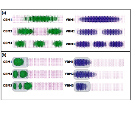
Figure 2 shows the real space contour plots of the three wavefunctions adjacent to the bandgap in the 3 nm CdSe quantum rod conduction and valence band. In Fig. 2(a) three wavefunctions are calculated for a free standing CdSe nanorod, while for Fig. 2(b) nanorod is embedded into the electrode (indicated by the semi-transparent rectangles) by one quarter of its length. In the latter case both CBM and VBM wavefunctions are localized by the polarization potential induced by the electrode. While for CBM states, the wavefunctions are just shrunk in the -direction, for VBM states the second and third states show different nodal structure in comparison with their free rod counterparts, indicating strong state mixing and crossing. Due to the electron and hole state localization, the transport properties of small nanorods measured with attached electrodes will be different from familiar free electron-like picture, and more resemble the case of the Coulomb blockade.
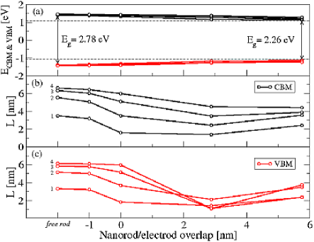
Another important consequence of the electrode induced polarization potential is the change in the value of the bandgap. Figure 3 shows the VBM and CBM states evolution as a function of the overlap between the nanorod and the electrode for the 3 nm diameter CdSe nanorod. In this case the value of the bandgap is reduced by approximately 0.5 eV (Fig.3(a)), from 2.78 eV to 2.26 eV as the rod is embedded into the electrode. The bangap value changes slightly when the nanorod and the electrode are separated by the 1 nm layer of vacuum ( eV). Once the electrode is in contact with the nanorod the change is more pronounced ( eV) and becomes more significant with increasing the electrode/nanorod overlap, eventually saturating. In the absence of the electrode, the polarization potential of a free standing nanorod induces the bandgap increase of 0.54 eV (from 2.24 eV to 2.78 eV) in comparison with the gap calculated ignoring the surface polarization (dashed lines in Fig.3). Thus, the existence of the electrode will also significantly affect the value of the quasiparticle band gap. Note that this quasiparticle bandgap equals the difference the electron affinity and ionization energy. It is different from the optical band gap. For optical band gap one has to include the electron-hole Coulomb interaction, which partially cancells out the polarization potential effects, especially for isolated spherical quantum dots.
In order to quantify the electrode induced localization of the electron and hole wavefunctions we define a localization function
| (6) |
where the wavefunction center of mass is . It shows how spread-out the wavefunction is throughout the nanorod. This localization is presented in Figure 3 (b) and (c), for CBM and VBM respectively as a function of the electrode/nanorod overlap. It is interesting to note that localization of the wavefunctions is different from that of the free standing nanorod already when the nanorod and the electrode are 1 nm apart. The localization becomes significant for both CBM and VBM when the electrode is in contact with the nanorod. Throughout the electrode/nanorod overlap range the electron states are less localized than the hole states due to the differences in their effective masses. As the electrode covers more of the rod length, wavefunctions become less localized since the width of the confining potential is increasing. Thus there is an optimal electrode-nanorod overlap for maximally localized electron/hole wavefunctions. For the 3 nm nanorod this optimal overlap appears to be around 3 nm.
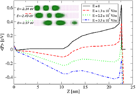
In order to make the electron mobile again, one can apply an electric field along the wire axis to overcome the wavefunction localization. To estimate the magnitude of this electric field we apply a linear potential drop to the total potential in Eq. 2 between the ends of the nanorod, and calculate the resulting electronic properties. This is demonstrated in Figure 4 where the weighted average of the polarization potential is plotted for 3 nm diameter CdSe nanorod embedded into the electrode by half of its length. The field of V/m (corresponding to a bias voltage of about 0.5 V applied across the 23 nm nanorod) is needed to delocalize the CBM wavefunction. The inset shows a representative (the third) CBM wavefunction contour plots for electric fields of 0, 1.3, and 2.2 V/m (bias voltages of 0, 0.3, and 0.5 V). The wavefunction in the latter case is dragged by the field towards the center of the rod, while its eigenvalue changes from -2.34 eV to -2.57 eV. Although it is no longer localized, it is still affected by the electrode, the structure of the wavefunction is not the same as in a free standing rod (compare to Fig. 2a).
In conclusion, using atomistic pseudopotential method combined with electrostatic polarization potential we have demonstrated the electrode induced localization of CBM and VBM states in CdSe nanorods (representing infinitely long nanowire). The effect is surprisingly large for small (1.5 - 3 nm diameter) nanorods but becomes insignificant as nanorod size grows (6 nm and up). The large polarization potential induced by the electrode also lead to the narrowing of the quasiparticle bandgap by 0.5 eV in 3 nm CdSe nanorods. We quantify the wavefunctions localization and compute the electric fields necessary to delocalize states near the CBM. We show that the mere presence of the electrode alters the nanorod electronic properties in comparison with a free standing nanorod, and this should be taken into account in interpreting the experimental transport measurements. This is a unique nanocontact phenomenon absent in its macroscopic counterpart.
In order to experimentally confirm the effect of electrode induced localization we propose a measurement using one of the established wavefunction mapping techniques, such as scanning tunneling microscopy (STM), along with a conductivity measurements for a series of small nanorods (1.5 - 3 nm diameter), embedded in the electrods by different degrees.
This work was supported by U.S. Department of Energy under Contract No.DE-AC02-05CH11231 and used the resources of the National Energy Research Scientific Computing Center (NERSC).
References
- Manna et al. (2003) L. Manna, D. J. Milliron, A. Miesel, E. C. Scher, and A. P. Alivisatos, Nature Materials 2, 382 (2003).
- Milliron et al. (2004) D. J. Milliron, S. M. Hughes, Y. Cui, L. Manna, J. Li, L. W. Wang, and A. P. Alivisatos, Nature 430, 190 (2004).
- Gao and Wang (2002) P. Gao and Z. L. Wang, J. Phys. Chem. B 106, 12653 (2002).
- Klein et al. (1997) D. L. Klein, R. Roth, A. K. L. Lim, A. P. Alivisatos, and P. L. McEuen, Nature 389, 699 (1997).
- Fang et al. (2007) L. Fang, J. Park, Y. Cui, J. Schrier, B. Lee, L.-W. Wang, A. P. Alivisatos, and M. Salmeron, J. Chem. Phys. p. submitted (2007).
- Steiner et al. (2005) D. Steiner, T. Mokari, U. Banin, and O. Millo, Phys. Rev. Lett 95, 056805 (2005).
- Heo et al. (2004) Y. W. Heo, L. C. Tien, D. P. Norton, B. S. Kang, F. Ren, B. P. Gila, and S. J. Pearton, Appl. Phys. Lett. 85, 2002 (2004).
- Cui et al. (2005) Y. Cui, U. Banin, M. T. Björk, and A. P. Alivisatos, Nano Letters 5, 1519 (2005).
- Thelander (2003) C. Thelander, Appl. Phys. Lett. 83, 2052 (2003).
- Zhang et al. (1999) Y. Zhang, T. Ichihashi, E. Landree, F. Nihey, and S. Lijima, Science 285, 1719 (1999).
- Gudiksen et al. (2002) M. S. Gudiksen, L. J. Lauhon, J. Wang, D. C. Smith, and C. M. Lieber, Nature 415, 617 (2002).
- Landman et al. (2004) U. Landman, R. N. Barnett, A. G. Scherbakov, and P. Avouris, Phys. Rev. Lett. 85, 1958 (2004).
- Wang (2005) L. W. Wang, J. Phys. Chem. B 109, 23330 (2005).
- Katz et al. (2002) D. Katz, T. Wizansky, O. Millo, E. Rothenberg, T. Mokari, and U. Banin, Phys. Rev. Lett. 89, 086801 (2002).
- Li and Alivisatos (2003) L. S. Li and A. P. Alivisatos, Phys. Rev. Lett. 90, 097402 (2003).
- LeThomas et al. (2005) N. LeThomas, E. Herz, O. Schöps, U. Woggon, and M. V. Artemyev, Phys. Rev. Lett. 94, 016803 (2005).
- Krishnan et al. (2004) R. Krishnan, M. A. Hahn, Z. Yu, J. Silcox, P. M. Fauchet, and T. D. Krauss, Phys. Rev. Lett. 92, 216803 (2004).
- Franceschetti and Zunger (2000) A. Franceschetti and A. Zunger, Phys. Rev. B 62, 2614 (2000).
- Rabani et al. (1999) E. Rabani, B. Hetényi, B. J. Berene, and L. E. Brus, J. Chem. Phys. 110, 5355 (1999).
- Stopa (1996) M. Stopa, Phys. Rev. B 54, 13767 (1996).
- Fonoberov et al. (2002) V. A. Fonoberov, E. P. Pokatilov, and A. A. Balandin, Phys. Rev. B 66, 085310 (2002).
- Wang and Zunger (1996) L. W. Wang and A. Zunger, Phys. Rev. B 53, 9579 (1996).
- Léonard and Talin (2006) F. Léonard and A. A. Talin, Phys. Rev. Lett. 97, 026804 (2006).
- Wang and Zunger (1994) L. W. Wang and A. Zunger, J. Chem. Phys. 100, 2394 (1994).
- Brus (1983) L. E. Brus, J. Chem. Phys. 79, 5566 (1983).
- Brus (1984) L. E. Brus, J. Chem. Phys. 80, 4403 (1984).
- Cartoixa and Wang (2005) X. Cartoixa and L. W. Wang, Phys. Rev. Lett. 94, 236804 (2005).