Reentrance effect in a graphene n-p-n junction coupled to a superconductor
Abstract
We study the interplay of Klein tunneling (= interband tunneling) between n-doped and p-doped regions in graphene and Andreev reflection (= electron-hole conversion) at a superconducting electrode. The tunneling conductance of an n-p-n junction initially increases upon lowering the temperature, while the coherence time of the electron-hole pairs is still less than their lifetime, but then drops back again when the coherence time exceeds the lifetime. This reentrance effect, known from diffusive conductors and ballistic quantum dots, provides a method to detect phase coherent Klein tunneling of electron-hole pairs.
pacs:
74.45.+c, 73.23.-b, 73.40.Lq, 74.50.+rThe conductance of a diffusive conductor increases if one of the electrodes becomes superconducting upon lowering the temperature, as a consequence of phase coherence between electron and hole excitations (Andreev pairs) induced by the proximity to the superconductor. The initial increase does not persist to the lowest temperatures. Instead, the normal-state value reappears when the thermal coherence length of the Andreev pairs exceeds the sample size. This is the so called reentrance effect, first observed a decade ago in a metal wireCha96 ; Chi99 and in a semiconductor two-dimensional electron gas.Har96 ; Toy99 (The theoretical prediction goes back much further.Naz96 ; Art79 ) The reentrance effect is now routinely used to measure the coherence time of Andreev pairs in a much wider class of diffusive conductors, see for example a recent experiment on multiwall carbon nanotubes.Har03 It has also been predicted to occur in a ballistic quantum dot with properly adjusted point contacts.Cle00 We refer to Ref. Cou99, for an extensive review of the topic and to Ref. Bee00, for a tutorial.
As pointed out by Silvestrov and Efetov,Sil07 a p-doped region in n-doped graphene (or, converselyly, an n-doped region in p-doped graphene) confines carriers in much the same way as a quantum dot in a two-dimensional electron gas. An electron in the valence band of the p-doped region can escape into the conduction band of the adjacent n-doped regions, by the process of Klein tunneling.Che06 ; Kat06 This interband tunneling process is highly directional: Only electrons near normal incidence are transmitted through a smooth n-p interface.Che06 The n-p interface thus functions as a constriction in momentum space, analogously to the constriction in real space formed by a point contact in a conventional quantum dot.
If an n-p junction is in series with a superconducting electrode, then the interband tunneling is combined with electron-hole conversion (known as Andreev reflectionAnd64 ) at the interface with the superconductor. Here we study the interplay of these two scattering mechanisms, and show that they lead to a reentrance effect in the temperature dependent conductance.
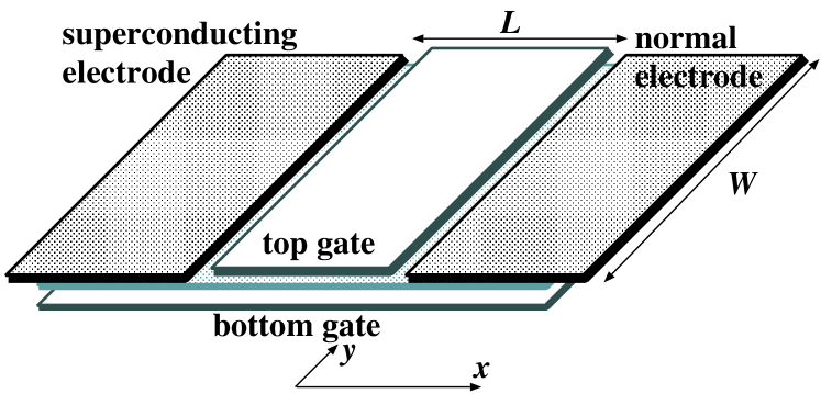
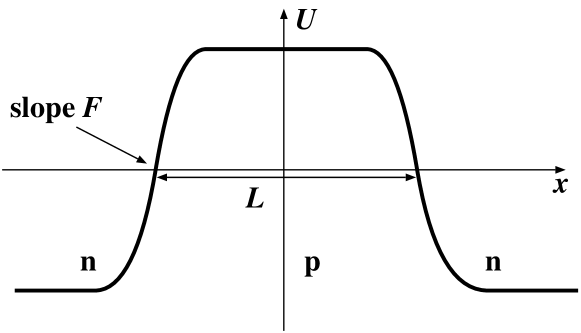
We consider a p-doped graphene strip (length , width ), connecting two n-doped regions (see Fig. 1). One n-region is contacted by a normal metal electrode, the other by a superconducting electrode. The electrostatic potential profile, controlled by a top gate and a bottom gate, is assumed to vary smoothly on the scale of the Fermi wave length. Close to the Fermi level (chosen at ) the potential energy increases as near the left n-p interface and decreases as near the right p-n interface. The slopes are of order , with the carrier velocity in graphene, the average of the Fermi wave vector at the two sides of the interface, and the thickness of the interface. For simplicity, we will take in the main text and consider the effects of two unequal interfaces at the end of the paper.
The tunnel probabilities per mode through a smooth p-n junction () have been calculated by Cheianov and Fal’ko:Che06
| (1) |
in terms of the transverse wave vector of the -th mode. These determine the tunnel conductance via the Landauer formula,
| (2) |
The total number of propagating modes in the p-doped region is , with the Fermi wave vector in that region. Only a relatively small number of these modes near normal incidence have close to 1. (In this sense a p-n interface forms a constriction in momentum space.) We assume that the number of open scattering channels is still , so that sums over may be replaced by integrations over : . The resulting tunnel conductance isChe06
| (3) |
Eq. (3) is the conductance of a p-n junction between two normal metal contacts. If one of the contacts is superconducting we can calculate the conductance from the formulaAkh07
| (4) |
Replacing again the sum over modes by an integration, this Andreev conductance evaluates to
| (5) |
The incoherent series conductance of the n-p-n junction between a superconducting and normal metal contact becomes
| (6) |
It is slightly larger than the series conductance when both contacts are in the normal state.
To determine the coherent series conductance we assume that the p-region is weakly disordered (mean free path ), such that the modes are randomized before the electron or hole escapes out of the p-doped region. We thus require that the scattering time is less than the dwell time , which is satisfied if (assuming ). During a time the carrier explores an area , with determined by the diffusion constant . The n-p-n junction corresponds statistically to quantum dots in parallel, each with open scattering channels. For we may use random-matrix theory to calculate the average density of transmission eigenvalues through this system. The difference between the symplectic ensemble appropriate for Dirac fermions in graphene and the orthogonal ensemble of a conventional quantum dot does not show up to leading order in , so we may ignore it and use the general result in the literature for the orthogonal ensemble,Bro96
| (7) |
Combining Eqs. (1) and (7), the coherent series conductance evaluates to
| (8) |
The crossover from coherent to incoherent series addition occurs when the thermal energy becomes comparable to the Thouless energy
| (9) |
with the mean level spacing (per spin and valley) in the p-region. In order of magnitude, . We assume that the gap in the superconducting reservoir is . From Eqs. (6) and (8) we expect a 2% decrease of the conductance upon lowering the temperature below . We will now show that this decrease is preceded by an increase, such that the conductance is maximal at .
To calculate this reentrance effect we may again use random-matrix theory, as in Ref. Cle00, , or we may use the equivalent circuit theory of quasiclassical Green’s functions,Naz99 as in Refs. Sam04, ; Big06, . Here we follow the latter approach. Just as in the random-matrix approach, no modification of the conventional circuit theory is needed to leading order in . In this quasiclassical limit the Green’s functions are represented by matrices acting in the Keldysh and Nambu spaces, as a function of position and momentum direction . Green’s functions for Dirac fermions have an additional structure from the valley and pseudospin degree of freedom,Khv06 ; McC06 which in the quasiclassical limit factors out:
| (10) |
[The Pauli matrices and act on the valley and pseudospin degree of freedom, respectively, and we take a basis in which the Dirac Hamiltonian is .]
The quasiclassical Green’s functions in the superconducting lead , in the normal lead , and in the n-p-n junction are matrices in the Keldysh space,Ram86
| (11) |
where , and are matrices in the Nambu space. In the leads they take their equilibrium values, depending only on the excitation energy :
| (12) | ||||
| (13) |
Here , with the applied voltage and the Fermi function. The Pauli matrices act in the Nambu space.
The Green’s function in the n-p-n junction has the form
| (14) |
The unknown parameters , can be found from the conservation law of the matrix current,Naz99
| (15) |
with the definitions
| (16) |
Here is a commutator, is an anticommutator, and the label stands for or .
From the retarded component of Eq. (15) we obtain an equation for ,
| (17) | ||||
| (18) |
The Keldysh component of Eq. (15) determines ,
| (19) |
The electrical current is related to the Keldysh component of the matrix current,
| (20) |
The zero temperature differential conductance is then given by
| (21) |
where is a solution of Eq. (17) at and is given by Eq. (19).
The result for is presented by a solid line in Fig. 2. In the limits and we recover, respectively, the incoherent limit (6) and the coherent limit (8). We find that takes a maximum value at . Fig. 3 (solid line) shows the temperature-dependent linear-response conductance
| (22) |
Again we observe nonmonotonic behavior with a maximum value at .
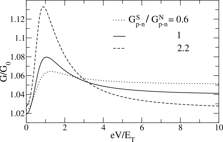
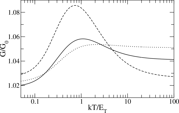
Figs. 2 and 3 also show results for the more general case of two unequal p-n interfaces, for several values of the ratio of the tunnel conductances. If the interface closest to the superconductor has a higher conductance than the other interface, then the reentrance effect is enhanced (dashed line), while it is reduced in the opposite case (dotted line). This dependence is analogous to that found in a conventional quantum dot.Cle00
In conclusion, we have shown that the conductance of a weakly disordered n-p-n junction in graphene coupled to a superconductor exhibits a reentrance effect, similar to what is found in diffusive conductors and ballistic quantum dots: The conductance takes approximately the same value at low and high voltages (or temperatures) and reaches a maximum when (or ) is approximately equal to the Thouless energy. This behavior should be observable in currently available graphene-superconductor junctionsHee07 and would provide a demonstration of phase-coherent Klein tunneling of electron-hole pairs.
We have benefited from discussions with A. R. Akhmerov, W. Belzig, and Yu. V. Nazarov. This research was supported by the Dutch Science Foundation NWO/FOM and by the German Science Foundation DFG through SFB 513.
References
- (1) P. Charlat, H. Courtois, Ph. Gandit, D. Mailly, A. F. Volkov, and B. Pannetier, Phys. Rev. Lett. 77, 4950 (1996).
- (2) C.-J. Chien and V. Chandrasekhar, Phys. Rev. B 60, 15356 (1999).
- (3) S. G. den Hartog, C. M. A. Kapteyn, B. J. van Wees, T. M. Klapwijk, and G. Borghs, Phys. Rev. Lett. 77, 4954 (1996).
- (4) E. Toyoda, H. Takayanagi, and H. Nakano, Phys. Rev. B 59, R11653 (1999).
- (5) Yu. V. Nazarov and T. H. Stoof, Phys. Rev. Lett. 76, 823 (1996).
- (6) S. N. Artemenko, A. F. Volkov, and A. V. Zaitsev, Solid State Comm. 30, 771 (1979).
- (7) J. Haruyama, K. Takazawa, S. Miyadai, A. Takeda, N. Hori, I. Takesue, Y. Kanda, N. Sugiyama, T. Akazaki, and H. Takayanagi Phys. Rev. B 68 165420 (2003).
- (8) A. A. Clerk, P. W. Brouwer, and V. Ambegaokar, Phys. Rev. B 62, 10226 (2000).
- (9) H. Courtois, P. Charlat, P. Gandit, D. Mailly, and B. Pannetier, J. Low Temp. Phys. 116, 187 (1999).
- (10) C. W. J. Beenakker, in: Quantum Mesoscopic Phenomena and Mesoscopic Devices in Microelectronics, edited by I. O. Kulik and R. Ellialtioglu, NATO Science Series C559 (Kluwer, Dordrecht, 2000). Online at arXiv:cond-mat/9909293.
- (11) P. G. Silvestrov and K. B. Efetov, Phys. Rev. Lett. 98, 016802 (2007).
- (12) V. V. Cheianov and V. I. Fal’ko, Phys. Rev. B 74, 041403(R) (2006).
- (13) M. I. Katsnelson, K. S. Novoselov, and A. K. Geim, Nature Phys. 2, 620 (2006).
- (14) A. F. Andreev, Sov. Phys. JETP 19, 1228 (1964).
- (15) C. W. J. Beenakker, Phys. Rev. B 46, 12841 (1992); for the applicability of the conductance formula (4) to the graphene-superconductor interface, see: A. R. Akhmerov and C. W. J. Beenakker, Phys. Rev. B 75, 045426 (2007).
- (16) P. W. Brouwer and C. W. J. Beenakker, J. Math. Phys. 37, 4904 (1996): Eq. (6.48).
- (17) Yu. V. Nazarov, Phys. Rev. Lett. 73, 134 (1994); Superlattices Microstruct. 25, 1221 (1999).
- (18) P. Samuelsson, W. Belzig, and Yu. V. Nazarov, Phys. Rev. Lett. 92, 196807 (2004).
- (19) G Bignon, F. Pistolesi, and M. Houzet, Eur. Phys. J. B 50, 465 (2006).
- (20) D. V. Khveshchenko, Phys. Rev. Lett. 97, 036802 (2006).
- (21) E. McCann, K. Kechedzhi, V. I. Fal’ko, H. Suzuura, T. Ando, and B. L. Altshuler, Phys. Rev. Lett. 97, 146805 (2006).
- (22) J. Rammer and H. Smith, Rev. Mod. Phys. 58, 323 (1986).
- (23) H. B. Heersche, P. Jarillo-Herrero, J. B. Oostinga, L. M. K. Vandersypen, and A. F. Morpurgo, Nature 446, 56 (2007).