Substrate temperature changes during MBE growth of GaMnAs
Abstract
Remarkably big increase of the substrate temperature during the low-temperature MBE growth of GaMnAs layers is observed by means of band gap spectroscopy. It is explained and simulated in terms of changes in the absorption/emission characteristics of the growing layer. Options for the temperature variation damping are discussed.
pacs:
81.05.Ea, 81.15.-zI Introduction
The growth temperature is an important parameter determining the quality of the MBE grown ferromagnetic GaMnAs layers. Its optimum value depends on the Mn doping level.Ohno ; Sadowski ; Camp03 With increasing Mn density the growth temperature has to be reduced in order to prevent the Mn precipitation. At the same time, however, a certain minimum temperature must not be underrun in order to maintain the 2D growth. The growth temperature adjustment is critical especially at high Mn doping levels where the temperature range of the 2D growth becomes narrow. Unfortunately, determining the substrate temperature at this temperature region is biased by a considerable uncertainty: the GaAs substrate is transparent for a low-temperature pyrometry, and a thermocouple can only weakly be linked to a rotating substrate holder. Moreover, it is difficult to eliminate a substantial delay in the temperature regulation.
Application of the diffuse reflectance spectroscopyBESthermo (or band edge spectroscopy, BES) not only allows one to overcome the above problems, but also reveals remarkable temperature changes connected with the massive Mn doping. Similar observation has already been reported in connection with growth of smaller band gap layers on larger band gap substrates,Shanabrook and with heat flux transients due to opening/closing the effusion cell shutters.Thompson The latter problem is certainly involved in our case, too. However, as we show further, yet another mechanism takes effect, becoming essential when growing heavily doped samples mounted in In-free sample holders.
II Experiment
The growth experiments were performed in Veeco Gen II MBE system. A semiinsulating m thick GaAs substrate with 2-inch diameter was mounted into a molybdenum In-free sample holder, fixed mechanically at its edge. No diffuser plate was used between the substrate and the heater. Distance between the heater (2-inch PBN plate with tungsten filament inside) and the substrate was about 10 mm. The band-edge spectrometer (kSA BandiT) was mounted on the central pyrometer port, normal to the substrate. In this arrangement the thermal radiation of the heater had sufficient intensity near the band-gap wavelengths to serve as a radiation source for the transmission measurement even at temperatures as low as 200∘C.
The low-temperature part of the structures under investigation consisted of 5 nm thick GaAs buffer and 150 nm thick layer, with x varying from 2.5% to 7%. At the growth rate used the temperature of the Ga source was 930∘C, the Mn source temperature varied from 770 to 830∘C. During the growth the substrate heater was supplied by a constant power, without any feedback temperature control. The same initial substrate temperature of C was reproduced when applying the same power and using always the same piece of sample holder.
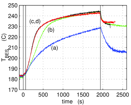
In Figure 1 temporal evolutions of the BES-measured substrate temperatures () are shown for growths with various Mn densities. All the curves have several common features: (i) small (less than 5 degrees) increase of after opening the Ga source; (ii) pronounced (40–60 degrees) increase after opening the Mn source; (iii) decrease after closing the sources, with a new steady-state value well above the initial substrate temperature. During all the growths the temperature measured by usual floating thermocouple behind the substrate showed only a weak increase (less than 3 degrees) which relaxed back after the growths.
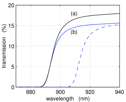
When considering the dramatic difference between the response to opening the Ga and Mn sources, a question arises on the validity of the BES interpretation as a change in substrate temperature. An alternative explanation could consist in a change of the transmission spectrum shape due to presence of Mn impurity levels close to the fundamental absorption edge. If it were so, a relevant difference would have to be detectable between spectra of an undoped GaAs and a GaMnAs layer at the same temperature. Two such spectra are shown in Fig. 2, representing a semiinsulating GaAs substrate, and the same substrate with a GaMnAs layer on top of it. In the band edge region, however, there appears to be no significant difference between the spectra, comparable to the expected shift due to difference in temperature.BESthermo ; Urbach Thus, the chemically induced spectrum change is unlikely in the relevant parameter range and the observed band edge shift can indeed be attributed to the change in temperature. The more the question recurs on the mechanism of the dramatic temperature increase after opening the Mn source.
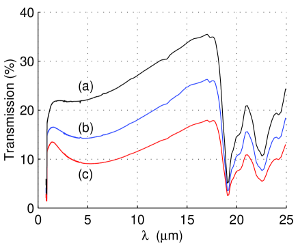
We attribute this effect to increasing heat absorption in the heavily doped epitaxial layer. Two straightforward absorption channels may be considered, related to the Mn doping: excitation of valence electrons to the Mn acceptor level, and free carrier absorption. The first channel can readily be neglected: with the ionization energy around 100 meV (Ref. Parker, ) the Mn atoms are almost fully occupied at the room temperature, making further transitions from the valence band impossible. On the other hand, the absorption efficiency via free holes is strong due to their extremely high density (in the order of cm-3). Since, moreover, their mobility is low and relaxation time short (in the order of 10 cm2/Vs, and s, respectively), a significant absorption can be expected in a broad infrared range, starting already in the GaAs bandgap.Cardona This is illustrated in Fig. 3 where transmission spectra between 1 and 25 m are shown for various samples.
Besides the free hole absorption the incoming heat is absorbed also by crystal lattice vibrations, independently of the doping. A strong two-phonon absorption is seen in the long-wavelength part of Fig. 3. This absorption and its one-phonon analogBlakemore around 35 m are mainly responsible for heating of an insulating GaAs substrate.heating
III Model
It is tempting to describe the heat exchange in the substrate simply as difference of (i) a heating term (proportional to heat flux from thermal sources, with an absorption factor increasing in time), and (ii) a cooling term (proportional to deviation from a steady state temperature). However, such a model turns out to be inadequate, yielding some results contradictory to experiments. For example, it predicts an unbounded increase of the substrate temperature, as long as the absorption increases, i.e. until the layer becomes completely opaque. Figures 1 and 3 show a different behavior: the temperature stabilizes in spite of the nonsaturated absorption. The reason of this failure is fundamental: according to Kirchhoff’s law the absorption efficiency of a body changes identically to its emission efficiency at each wavelength,Lienhard i.e. no temperature change can occur unless the radiation spectrum changes. Disregarding the spectral distribution in a system with significant radiative coupling, as in the above model, inevitably leads to nonphysical solutions.
A mathematical model we propose assumes fully radiative heat exchange. Its essential ingredients are proper description of the spectral power distributions of the thermal sources involved, and the doping induced change in the absorption and emission characteristics of the substrate.
A radiating and absorbing body can be approximated by a black body with spectral radiance (monochromatic emissive power) enclosed by a surface with dimensionless emittance and absorptance . The radiance obeys the Planck law,
| (1) |
The net heat transferred from a radiating body 1 to an absorbing/radiating body 2 can then be described as
| (2) |
where dimensionless factor represents the geometric configuration of the two bodies, is the surface area of body 2. This general principle can be used to describe — pair by pair — the heat exchange between the substrate and all other relevant thermal sources in the growth chamber.
To simplify the description we adopt the following assumptions:
(i)
emittance of each body equals to its absorptance,
(diffuse form of Kirchhoff’s
lawLienhard );
(ii)
the heater and the cells behave like gray bodies, i.e. their
emittances are constants;
(iii) absorptance/emittance of the substrate
is composed of the phonon and the free carrier contributions.
For simplicity, the phonons are assumed to absorb perfectly in their
wavelength interval(s), ,
the free carrier contribution is assumed
to rise in time, starting from zero in the undoped substrate and
exponentially saturating as the total number of free holes increases,
| (3) |
where the rate constant is proportional to dopant flux.
The following bodies are relevant for the heat exchange: the substrate heater (temperature ), the effusion cells opened during the growth (effective temperature ), the background of the growth chamber (effective temperature ), and the substrate (temperature ). The view factor for each pair of bodies can be approximated by the solid angles , , , at which the substrate with area ”sees” the respective bodies; identity holds, as the heater covers one complete hemisphere of the substrate’s scope (), the other hemisphere being filled by the background () with small hot spots of the opened cells (). The heat balance in the substrate is then
| (4) | |||||
Absorptance is a piecewise constant function, with its phonon part lying in a narrow interval in the mid infrared range. There the Planck’s law approximates to (Rayleigh-Jeans law), leading to linear terms in when integrating Eq. (4), whereas the complete Planck’s law yields terms proportional to . Thence, equation (4) after integration results in
where is the Stefan-Boltzmann constant, is the view angle ratio of the opened cells, and . The constant factor reflects the ratio of power irradiated in the phonon domain and power over all wavelengths,
| (6) |
Taking m and m leads to as an order of magnitude estimate.myphonon
In equilibrium, , and Eq. (LABEL:qnet) determines the steady state substrate temperature for any given , , , and ; parameters and are physical and technical constants, respectively. Out of equilibrium, the temporal evolution of is governed by
| (7) |
where is constant heat capacity of the GaAs substrate; varying electronic specific heat can safely be neglected at the relevant temperatures.Ashcroft Let us note that if the change in temperature is slow enough the system remains quasistationary and can still be find alone by solving with increasing in time according to Eq. (3).
Explicit solutions can be obtained in two special stationary cases:
a) Negligible free electron absorption, or .
Equation (LABEL:qnet) simplifies to
| (8) |
In particular, in the steady state before the growth,
when .
b) Prevailing free electron absorption, or
. Then,
| (9) |
In particular, in the steady state after the growth, explaining the persistent increase of as a consequence of change of the absorption characteristic in presence of two different thermal sources.
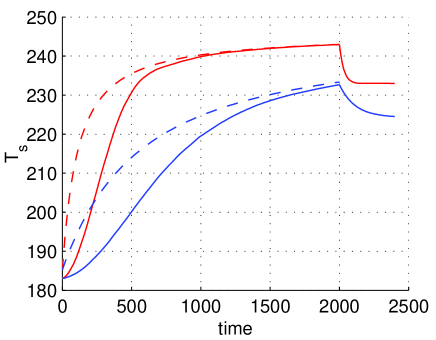
The above stationary solutions can be used to determine the model parameters from the measured data. In accordance with Fig. 1 we can take C before the growth, C at the end of the growth of the most strongly doped layer, and C long after closing the cells. Taking further as a rough estimate of the view angle ratio of the opened cells, we can solve Eqs. (8) and (9), getting C for the substrate heater temperature, C for the effective temperature of the opened cells, and C for the effective background temperature. This single set of plausible model parameters yields quasistationary solutions for shown in Fig. 4 by dashed lines, if we chose () as the doping rate constant of the strongly (weakly) doped layer. Trying, finally, (corresponding to 2-inch GaAs substrate of m thickness), Eqs. (LABEL:qnet) and (7) lead to time evolutions plotted by solid lines in Fig. 4.
IV Discussion
On account of its simplifications the model cannot have the ambition of a perfect agreement. Its main virtue lies in the fact that it links up parameters of a straightforward physical meaning with the observed temperature evolution, and that physically reasonable values of the model parameters lead to expectable results.
The accuracy of the agreement could be arbitrarily increased, e.g., by including additional thermal sources in the growth chamber and by tuning their temperatures. This, however, would not necessarily make the model more realistic. There are numerous influences out of reach of a simple description. For example, a part of the heat exchange is due to a conduction between the sample holder and other massive parts of the holder mechanism, all of them with particular heat capacities; the free electron absorption is wavelength dependent in the IR range; all surfaces exposed to material fluxes change their absorptance/emissivity during the growth, leading to changes of their temperatures; neither the phonon domain is absolutely absorbing, nor the near infrared absorption is completely absent in the undoped substrate; reflection takes place, etc.
The increase in the
substrate temperature is hardly visible for the floating
thermocouple behind the substrate, and a temperature
control based on it is thus inefficient. Yet, it is
desirable to keep the temperature change small,
especially in highly doped GaMnAs layers, where the growth
temperature is strongly constrained both from the
bottom (disordered condensation) and the top (precipitation).
Several schemes can be applied to meet this goal:
1. BES-locked substrate heater control;
2. anticipatory throttling of the substrate heater;
3. In-bonding of the substrate to a massive sample holder
with inherently strong IR absorption;
4. incorporation of a less doped (uncritical in temperature)
but sufficiently absorbing GaMnAs sublayer between the GaAs
substrate and the final GaMnAs structure.
Temperature evolutions of the In-bonded substrate and the structure with the buried GaMnAs heating layer are shown in Fig. 5. The curves clearly differ in their time constants, corresponding to different heat capacities. The temperature increase, however, is almost identical in both systems, reduced to less than one half if compared with Fig. 1.
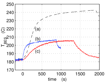
This illustrates an important difference between systems possessing a significant IR absorptance (such as In-bonded substrates, or sandwiched structures with buried heating layer), and systems where a wide-range IR absorptance is missing (such as In-free mounted semiinsulating substrates). In the first case the temperature increase is solely due to activation of an additional thermal source; wide-range IR absorption is already prevailing and its further change (if any) does not affect the heat-exchange balance. In terms of the presented model, terms linear in are negligible against terms .
In the second case the change of the spectrum of the substrate absorptance/emittance is essential; the change in temperature corresponds to a shift of the absorption maximum from longer to shorter wavelengths. In terms of the model, at first the main heat exchange takes places through terms linear in , later the terms prevail. The corresponding temperature increase would occur even if no additional heat flux appears. On the other hand, in a system with negligible absorption towards the shorter wavelengths, opening a high temperature cell with small orifice has little or no effect on the absorbed heat. Thus, an interesting paradox can occur: temperature variations in an In-bonded substrate can turn bigger than those in an In-free mounted substrate with weak free-carrier absorption.
V Summary
The main part of the dramatic increase in the substrate
temperature could unambiguously be connected with the
heavy Mn doping via the following scenario:
(i) Before the growth, the undoped substrate
absorbs the radiation from the thermal sources mainly
in the mid-infrared range (phonon domain).
(ii) The doping leads to strongly enhanced
free-carrier absorption in the near-infrared range,
shifting the decisive spectral absorptance
towards the shorter wavelengths.
(iii) More heat is absorbed from the high-temperature
(short wavelength) sources. To reach a new heat-exchange
equilibrium, the substrate radiance has to shift accordingly,
i.e. its temperature increases.
The proposed model, in contrast to a linear cooling model, explains all the main features of the observed effect, while preserving the involved physical mechanisms disclosed. Using plausible values of the input parameters it leads to quantitatively correct results. It yields conclusions relevant also for temperature stability during the MBE growth generally. Especially, it sheds a new light on behavior of In-bonded and In-free mounted substrates.
Acknowledgements.
We greatfully acknowledge stimulating discussions with R.P. Campion, as well as his contribution to the early stages of this work. The work was done in the framework of AV0Z1-010-914 program, supported by grants GACR 202/04/1519, ASCR KAN400100625, MoE LC510, and FON/06/E002 (ESF Eurocores-FoNE ERAS-CT-2003-980409).References
- (1)
- (2) H. Ohno, Science 281, 951 (1998)
- (3) J. Sadowski, J.Z. Domagala, J. Bak-Misiuk, S. Kolesnik, M. Sawicki, K. Swiatek, J. Kanski, L. Ilver, V. Ström, J. Vac. Sci. Technol. 18, 1697 (2000).
- (4) R.P. Campion, K.W. Edmonds, L.X. Zhao, K.Y. Wang, C.T. Foxon, B.L. Gallagher, C.R. Staddon, Journal of Crystal Growth 251, 311 (2003).
- (5) S.R. Johnson, C. Lavoie, T. Tiedje, J.A. Mackenzie, J. Vac. Sci. Technol. B11, 1007 (1993)
- (6) B. V. Shanabrook, J. R. Waterman, J. L. Davis, and R. J. Wagner, App. Phys. Letters 61, 2338 (1992)
- (7) P. Thompson, Y. Li, J.J. Zhou, D.L. Sato, L. Flanders, H.P. Lee, Appl. Phys. Lett. 70, 1605 (1997)
- (8) S.R. Johnson, T. Tiedje, J. Appl. Phys. 78, 5609 (1995)
- (9) E.H.C. Parker (ed.), The technology and physics of molecular beam epitaxy. (Plenum Press, N.Y., 1985), pp.78, 133
- (10) P.Y. Yu, M. Cardona, Fundamentals of Semiconductors, 1st ed. (Springer-Verlag Berlin Heidelberg, 1996), pp. 296-297.
- (11) J.S. Blakemore, J. Appl. Phys. 53, R123-R181 (1982)
- (12) J.H. Lienhard IV, J.H. Lienhard V, A heat transfer textbook. (Phlogiston Press, Cambridge, USA, 2006), p. 534
- (13) The interband absorption is negligible: a substrate heater at 300∘C radiates by factor 10-6 less power in the band gap region than in the one and two phonon regions.
- (14) N.W. Ashcroft, N.D. Mermin, Solid State Physics. (Brooks/Cole, 1976), pp. 463-464.
- (15) Used wavelengths correspond to two-phonon domain according to Ref.Blakemore, ; one phonon domain has been neglected. Using the somewhat longer wavelengths according to Fig. 3 one would obtain .