Electromigrated nanoscale gaps for surface-enhanced Raman spectroscopy
Abstract
Single-molecule detection with chemical specificity is a powerful and much desired tool for biology, chemistry, physics, and sensing technologies. Surface-enhanced spectroscopies enable single molecule studies, yet reliable substrates of adequate sensitivity are in short supply. We present a simple, scaleable substrate for surface-enhanced Raman spectroscopy (SERS) incorporating nanometer-scale electromigrated gaps between extended electrodes. Molecules in the nanogap active regions exhibit hallmarks of very high Raman sensitivity, including blinking and spectral diffusion. Electrodynamic simulations show plasmonic focusing, giving electromagnetic enhancements approaching those needed for single-molecule SERS.
Multifunctional sensors with single-molecule sensitivity are greatly desired for a variety of sensing applications, from biochemical analysis to explosives detection. Chemical and electromagnetic interactions between molecules and metal substrates are used in surface-enhanced spectroscopiesMoskovits85RMP to approach single molecule sensitivity. Electromagnetic enhancement in nanostructured conductors results when incident light excites local electronic modes, producing large electric fields in a nanoscale region, known as a “hot spot”, that greatly exceed the strength of the incident field. Hot spots can lead to particularly large enhancements of Raman scattering, since the Raman scattering rate is proportional to at the location of the molecule, where is the electric field component at the frequency of the incident radiation, and is the component at the scattered frequency.
It has been an ongoing challenge to design and fabricate a substrate for systematic SERS at the single molecule level. Single-molecule SERS sensitivity was first clearly demonstrated using random aggregates of colloidal nanoparticlesKneippetAl97PRL ; NieetAl97Science ; XuetAl99PRL ; MichaelsetAl00JPCB . Numerous other metal substrate configurations have been used for SERS, including chemically engineered nanoparticlesJacksonetAl04PNAS ; WangetAl05JACS ; OldenburgetAl99JCP , nanostructures defined by bottom-up patterningHaynesetAl01JPCB ; QinetAl06PNAS , and those made by traditional lithographic approachesFrommetAl06JCP . In the most sensitive substrate geometries, incident light excites adjacent subwavelength nanoparticles or nanostructures, resulting in large field enhancements within the interparticle gapHallocketAl05PNAS ; NordlanderetAl04NL . Fractal aggregates of nanoparticlesWangetAl03PNAS can further increase field enhancements by focusing plasmon energy from larger length scales down to particular nanometer-scale hotspotsLietAl03PRL . However, precise and reproducible formation of such assemblies in predetermined locations has been extremely challenging. An alternative approach is tip-enhanced Raman spectroscopy (TERS), in which the incident light excites an interelectrode plasmon resonance localized between a sharp, metal scanned probe tip and an underlying metal substrate. Recent progress has been made in single-molecule TERS detectionDomkeetAl06JACS ; NeascuetAl06PRB ; ZhangetAl07JPCC . A similar approach was recently attempted using a mechanical break junctionTianetAl06JACS . While useful for surface imaging, TERS requires feedback to control the tip-surface gap, and is not scalable or readily integrated with other sensing modalities.
We demonstrate a scaleable and highly reliable method for producing planar extended electrodes with nanoscale spacings that exhibit very large SERS signals, with each electrode pair having one well-defined hot spot. Confocal scanning Raman microscopy demonstrates the localization of the enhanced Raman emission. The SERS response is consistent with a very small number of molecules in the hotspot, showing blinking and spectral diffusion of Raman lines. Sensitivity is sufficiently high that SERS from physisorbed atmospheric contaminants may be detected after minutes of exposure to ambient conditions. The Raman enhancement for -mercaptoaniline (MA) is estimated from experimental data to exceed . Finite-difference time-domain (FDTD) modeling of realistic structures reveals a rich collection of interelectrode plasmon modes that can readily lead to SERS enhancements as large as over a broad range of illumination wavelengths. These structures hold the promise of integration of single-molecule SERS with electronic transport measurements, as well as other near-field optical devices.
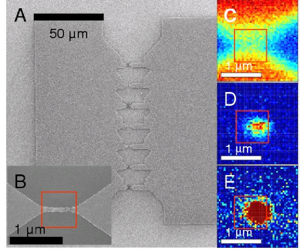
Our structures are fabricated on a Si wafer topped by 200 nm of thermal oxide. Electron beam lithography is used to pattern “multibowtie” structures as shown in Fig. 1A. The multibowties consist of two larger pads connected by multiple constrictions, as shown. The constriction widths are 80-100 nm, readily within the reach of modern photolithography. After evaporation of 1 nm Ti and 15 nm Au followed by liftoff in acetone, the electrode sets are cleaned of organic residue by exposure to O2 plasma for 1 minute. The multibowties are placed in a vacuum probe station, and electromigrationParketAl99APL is used to form nanometer-scale gaps in the constrictions in parallel, as shown in Fig. 1B. Electromigration is a nonthermal process whereby momentum transfer from current-carrying electrons is transferred to the lattice, rearranging the atomic positions. Electromigration has been studied thoroughlyStrachanetAl05APL ; TrouwborstetAl06JAP ; StrachanetAl06NL ; TaychatanapatetAl07NL as a means of producing electrodes for studies of single-molecule conduction. We have performed manual and automated electromigration at room temperature, with identical results. The number of parallel constrictions in a single multibowtie is limited by the output current capacity of our electromigration voltage source. A post-migration resistance of 10 k for the structure in Fig. 1A appears optimal.
Post-migration high resolution scanning electron microscopy (SEM) shows interelectrode gaps ranging from too small to resolve to several nanometers. There are no detectable nanoparticles in the gap region or along the electrode edges. Based on electromigration of 283 multibowties (1981 individual constrictions), 77% of multibowties have final resistances less than 100 k, and 43% have final resistances less than 25 k. We believe that this yield, already high, can be improved significantly with better process control, particularly of the lithography and liftoff.
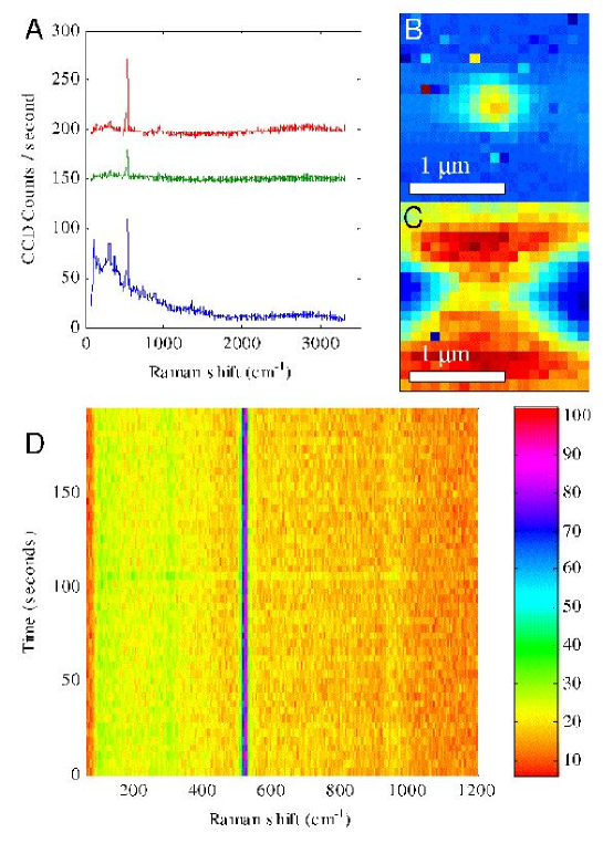
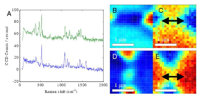
The optical properties of the resulting nanogaps are characterized using a WITec CRM 200 scanning confocal Raman microscope in reflection mode, with normal illumination from a 785 nm diode laser. Using a 100 objective, the resulting diffraction-limited spot is measured to be gaussian with a full-width at half-maximum of 575 nm. Fig. 1C shows a spatial map of the integrated emission from the 520 cm-1 Raman line of the Si substrate. The Au electrodes are clearly resolved. Polarization of the incident radiation is horizontal in this figure. Rayleigh scattered light from these structures shows significant changes upon polarization rotation, while SERS response is approximately independent of polarization.
Freshly cleaned nanogaps show no Stokes-shifted Raman emission out to 3000 cm-1. However, in 65% of clean nanogaps examined, a broad continuum background (see Supporting Information) is seen, decaying roughly linearly in wavenumber out to 1000 cm-1 before falling below detectability. This background is spatially localized to a diffraction-limited region around the interelectrode gap and is entirely absent in unmigrated junctions. The origin of this continuum, similar to that seen in other strongly enhancing SERS substratesMichaelsetAl00JPCB , is likely inelastic electronic effects in the gold electrodesBeversluisetAl03PRB . In samples coated with molecules, this background correlates strongly with visibility of SERS. No junctions without this background displayed SERS signals. Like the SERS signal, this background is approximately polarization independent. Temporal fluctuations of this background in clean junctions are minimal, strongly implying that fluctuations of the electrode geometry are not responsible for SERS blinking.
The SERS enhancement of the junctions has been tested using various molecules. The bulk of testing utilized MA, which self-assembles onto the Au electrodes via standard thiol chemistry. Particular modes of interest are carbon ring modes at 1077 cm-1 and 1590 cm-1. Fig. 1D shows a map of the Raman emission from the 1077 cm-1 line on the same junction as Fig. 1B,C, after self-assembly of MA. This emission is strongly localized to the position of the nanogap. No Raman signal is detectable either on the metal films or at the edges of the metal electrodes. Fig. 1E shows the spatial localization of the continuum background mentioned above.
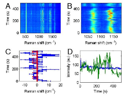
Fig. 2 shows a more detailed examination of the SERS response of the gap region of a typical junction after self-assembly of MA. Fig. 2A,B are time series of the SERS response, with known MA modes indicated. The modes visible are similar to those seen in other SERS measurements of MA on lithographically fabricated Au structuresFrommetAl06JCP . Each spectrum was acquired with 1 s integration time, with the objective positioned over the center of the nanogap hotspot. Temporal fluctuations of both the Raman intensity (“blinking”) and Raman shift (spectral diffusion), generally regarded as hallmarks of few- or single-molecule SERS sensitivityWangetAl05JPCB , are readily apparent. Fig. 2C shows a comparison of the wandering of the 1077 cm-1 MA line with that of the 520 cm-1 Raman line of the underlying Si substrate over the same time interval. This demonstrates that the spectral diffusion is due to changes in the molecular environment, rather than a variation in spectrometer response. Fig. 2D shows the variation in the peak amplitudes over that same time interval.
This blinking and spectral diffusion are seen routinely in these junctions. We have observed such Raman response from several molecules, including self-assembled films of MA, -mercaptobenzoic acid (MBA), a Co-containing transition metal complexCiszeketAl06JACS , and spin-coated poly(3-hexylthiophene) (P3HT). These molecules all have distinct Raman responses and show blinking and wandering in the junction hotspots.
Another indicator of very large enhancement factors in these structures is sensitivity to exogenous, physisorbed contamination. Carbon contamination has been discussedKudelskietAl00CPL ; Otto02JRS ; RichardsetAl03JRS in the context of both SERS and TERS. This substrate is sensitive enough to examine such contaminants (see Supporting Information). While clean junctions with no deliberately attached molecules initially show only the continuum background, gap-localized SERS signatures in the carbon region between 1000 cm-1 and 1600 cm-1 are readily detected after exposure to ambient lab conditions for tens of minutes. Nanojunctions that have been coated with a self-assembled monolayer (SAM) (for example, MA) do not show this carbon signature, even after hours of ambient exposure. Presumably this has to do with the extremely localized field enhancement in these structures, with the SAM sterically preventing physisorbed contaminants from entering the region of enhanced near field.
Recently arrived contaminant SERS signatures abruptly disappear within tens of seconds at high incident powers (1.8 mW), presumably due to desorption. SERS from covalently bound molecules is considerably more robust, degrading slowly at high powers, and persisting indefinitely for incident powers below 700 W. SEM examination of the nanogaps shows no optically induced damage after exposure to intensities that would significantly degrade nanoparticlesSchucketAl05PRL . The large extended pads likely aid in the thermal sinking of the nanogap region to the substrate.
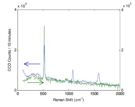
Estimating enhancement factors rigorously is notoriously difficult, particularly when the hotspot size is not known. Although SERS enhancement volume measurements are possible using molecular rulersLaletAl06NL , this is not feasible with such small nanogaps. Junctions made directly on Raman-active substrates (Si with no oxide; GaAs) show no clearly detectable enhancement of substrate modes in the gap region, suggesting that the electromagnetic enhancement is strongly confined to the thickness of the metal film electrodes. Figure 3 shows a comparison between a typical MA SERS spectrum acquired on a junction with a 600 s integration time at 700 W incident power, and a spectrum acquired over one of that device’s Au pads, for the same settings. The pad spectrum shows no detectable MA features and is dark current limited.
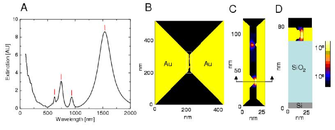
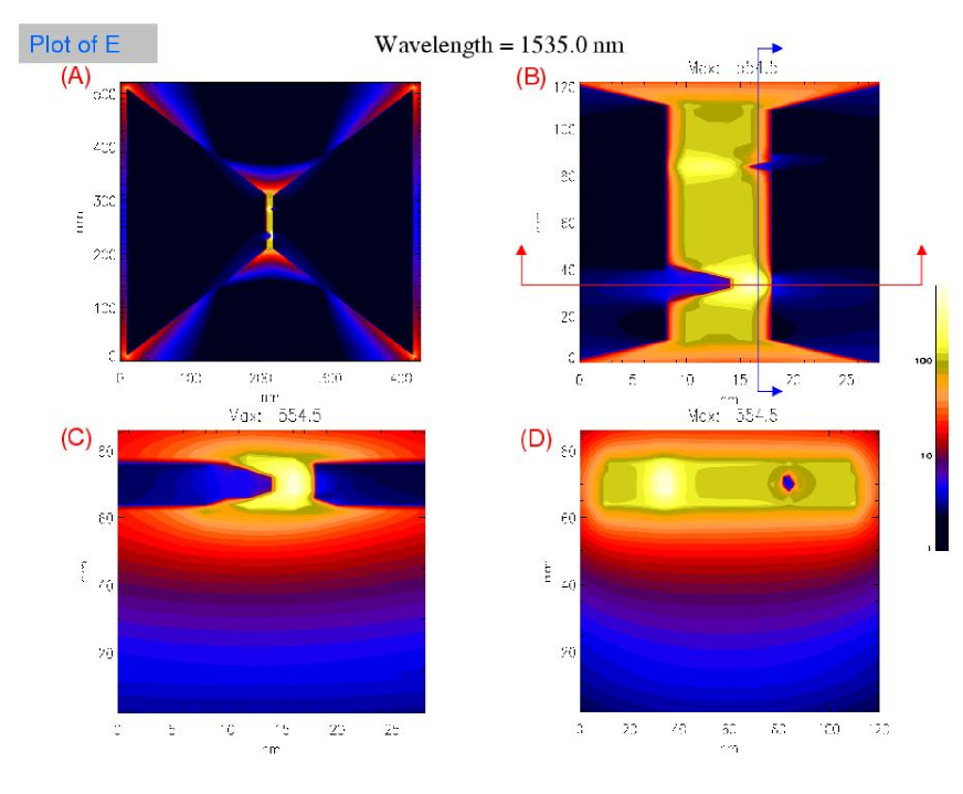
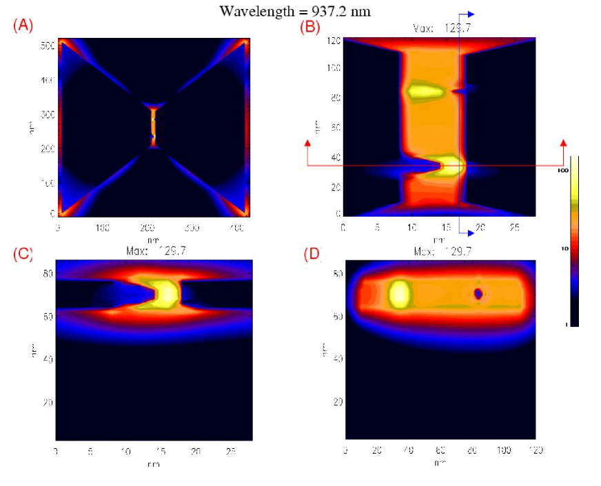
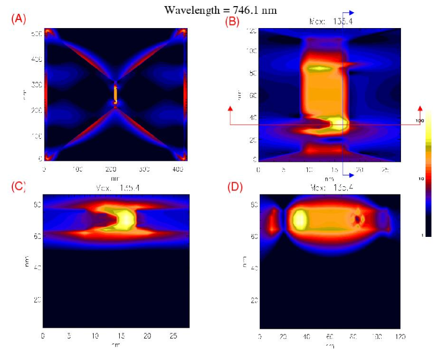
We use FDTD calculations to understand the strong SERS response in these structures and roughly estimate enhancement factors. It is important to note that the finite grid size (2 nm) required for practical computation times restricts the quantitative accuracy of these calculations. However, the main results regarding spatial mode structure (allowing assessment of the localization of the hotspot) and energy dependence are robust to these concerns, and the calculated electric field enhancement is an underestimateOubreNordlander05JPCB . Fig. 4 shows a calculated extinction spectrum and map of in the vicinity of the junction. Calculational details and additional plots are presented in the Supporting Information. These calculations predict that there should be large SERS enhancements across a broad bandwidth of exciting wavelengths because of the complicated mode structure possible in the interelectrode gap. Nanometer-scale asperities from the electromigration process break the interelectrode symmetry of the structure. The result is that optical excitations at a variety of polarizations can excite many interelectrode modes besides the simple dipolar plasmon commonly considered. For extended electrodes, a continuous band of plasmon resonances coupling to wavelengths from 500-1000 nm is expectedNordlanderLe06APB . This broken symmetry also leads to much less dependence of the calculated enhancement on polarization direction, as seen experimentally. The calculations confirm that the electromagnetic enhancement is confined in the normal direction to the film thickness. Laterally, the field enhancement is confined to a region comparable to the radius of curvature of the asperity. For gaps and asperities in the range of 2 nm, purely electromagnetic enhancements can exceed , approaching that sufficient for single-molecule sensitivity.
Using the data from the device in Fig. 3, we estimate the total enhancement in that device. To be conservative, we assume a hotspot effective radius of 2.5 nm with dense packing of MA, giving molecules. Blinking and wandering suggest that the true value is much closer to one. The integrated Raman signal over a gaussian fit to the 1077 cm-1 Raman line is 2.0 counts/sec/molecule when the incident power is 700 W. For our apparatus the count rate from imaging a bulk crystal at the same equivalent power (see Supporting Information) is counts/sec/molecule, so that we estimate a total enhancement of at least .
We have demonstrated a SERS substrate capable of extremely high sensitivity for trace chemical detection. Unlike previous substrates, these nanojunctions may be mass fabricated in controlled positions with high yield using a combination of standard lithography and electromigration. The resulting hotspot geometry is predicted to allow large SERS enhancements over a broad band of illuminating wavelengths. Other nonlinear optical effects should be observable in these structures as well. The extended electrode geometry and underlying gate electrode are ideal for integration with other sensing modalities such as electronic transport. Tuning molecule/electrode charge transfer via the gate electrode may also enable the direct examination of the fundamental nature of chemical enhancement in SERS.
DW acknowledges support from the NSF-funded Integrative Graduate Research and Educational Training (IGERT) program in Nanophotonics. NH, PN, and DN acknowledge support from Robert A. Welch Foundation grants C-1220, C-1222, and C-1636, respectively. DN also acknowledges the National Science Foundation, the David and Lucille Packard Foundation, the Sloan Foundation, and the Research Corporation. C.S.L. was supported by a training fellowship from the Keck Center Nanobiology Training Program of the Gulf Coast Consortia, NIH 1 T90 DK070121-01. YP and NKG are supported by US Army Research Office grant W911NF-04-1-0203.
Supporting Information Available: Detailed examination of continuum background and adsorption of exogenous contaminants; extended discussion of FDTD calculations; more detailed discussion of SERS enhancement calculation. This material is available free of charge via the Internet at http://pubs.acs.org.
References
- (1) Moskovits, M. Rev. Mod. Phys. 1985, 57, 783-826.
- (2) Kneipp, K.; Wang, Y.; Kneipp, H.; Perelman, L. T.; Itzkan, I.; Dasari, R. R.; Feld, M. S. Phys. Rev. Lett. 1997, 78, 1667-1670.
- (3) Nie, S.; Emory, S. R. Science 1997, 275, 1102-1106.
- (4) Xu, H.; Bjerneld, E. J.; Käll, M.; Börjesson, L. Phys. Rev. Lett. 1999, 83 4357-4360.
- (5) Michaels, A. M.; Jiang, J.; Brus, L. J. Phys. Chem. B 2000, 104, 11965-11971.
- (6) Jackson, J. B.; Halas, N. J. Proc. Nat. Acad. Sci. U.S.A. 2004, 101, 17930-17935.
- (7) Wang, H.; Levin, C. S.; Halas, N. J. J. Am. Chem. Soc. 2005, 127, 14992-14993.
- (8) Oldenburg, S. J.; Westcott, S. L.; Averitt, R. D.; Halas, N. J. J. Chem. Phys. 1999, 111, 4729-4735.
- (9) Haynes, C. L.; Van Duyne, R. P. J. Phys. Chem. B 2001, 105, 5599-5611.
- (10) Qin, L.; Zou, S.; Xue, C.; Atkinson, A.; Schatz, G. C.; Mirkin, C. A., Proc. Nat. Acad. Sci. U.S.A. 2006, 103, 13300-13303.
- (11) Fromm, D. P.; Sundaramurthy, A.; Kinkhabwala, A.; Schuck, P. J.; Kino, G. S.; Moerner, W. E. J. Chem. Phys. 2006, 124, 061101.
- (12) Hallock, A. J.; Redmond, P. L.; Brus, L. E. Proc. Nat. Acad. Sci. U.S.A. 2005, 102, 1280-1284.
- (13) Nordlander, P.; Oubre, C.; Prodan, E.; Li, K.; Stockman, M. I. Nano Lett. 2004, 4, 899-903.
- (14) Wang, Z.; Pan, S.; Krauss, T. D.; Du, H.; Rothberg, L. J. Proc. Nat. Acad. Sci. U.S.A. 2003, 100, 8638-8643.
- (15) Li, K.; Stockman, M. I., Bergman, D. J. Phys. Rev. Lett. 2003, 91, 227402.
- (16) Domke, K. F.; Zhang, D.; Pettinger, B. J. Am. Chem. Soc. 2006, 128, 14721-14727.
- (17) Neascu, C. C.; Dreyer, J.; Behr, N.; Raschke, M. B. Phys. Rev. B 2006, 73, 193406.
- (18) Zhang, W.; Yeo, B. S.; Schmid, T.; Zenobi, R. J. Phys. Chem. C 2007, 111, 1733-1738.
- (19) Tian, J.-H.; Liu, B.; Li, X.; Yang, Z.-L.; Ren, B.; Wu, S.-T.; Tao, N.; Tian, Z.-Q. J. Am. Chem. Soc. 2006, 128, 14748-14749.
- (20) Park, H.; Lim, A. K. L.; Alivisatos, A. P.; Park, J.; McEuen, P. L. Appl. Phys. Lett. 1999, 75, 301-303.
- (21) Strachan, D. R.; Smith, D. E.; Johnston, D. E.; Park, T. H.; Therien, M. J.; Bonnell, D. A., Johnson, A. T. Appl. Phys. Lett. 2005, 86, 043109.
- (22) Trouwborst, M. L.; van der Molen, S. J.; van Wees, B. J. J. Appl. Phys. 2006, 99, 114316.
- (23) Strachan, D. R.; Smith, D. E.; Fischbein, M. D.; Johnston, D. E.; Guiton, B. S.; Drndic, M.; Bonnell, D. A., Johnson, A. T. Nano Lett. 2006, 6, 441-444.
- (24) Taychatanapat, T.; Bolotin, K. I.; Kuemmeth, F.; Ralph, D. C. Nano Lett. 2007, 7, 652-656.
- (25) Beversluis, M. R.; Bouhelier, A.; Novotny, L. Phys. Rev. B 2003, 68, 115433.
- (26) Wang, Z.; Rothberg, L. J. J. Phys. Chem. B 2005, 109, 3387-3391.
- (27) Osawa, M.; Matsuda, N.; Yoshii, K.; Uchida, I. J. Phys. Chem. 1994, 98, 12702-12707.
- (28) Ciszek, J. W.; Keane, Z. K.; Cheng, L.; Stewart, M. P.; Yu, L. H.; Natelson, D.; Tour, J. M. J. Am. Chem. Soc. 2006, 128, 3179-3189.
- (29) Kudelski, A.; Pettinger, B. Chem. Phys. Lett. 2000, 321, 356-362.
- (30) Otto, A. J. Raman Spectrosc. 2002, 33, 593-598.
- (31) Richards, D.; Milner, R. G.; Huang, F.; Festy, F. J. Raman Spectrosc. 2003, 34, 663-667.
- (32) Schuck, P. J.; Fromm, D. P.; Sundaramurthy, A.; Kino, G. S.; Moerner, W. E. Phys. Rev. Lett. 2005, 94, 017402.
- (33) Lal, S.; Grady, N. K.; Goodrich, G. P.; Halas, N. J. Nano Lett. 2006, 6, 2338-2343.
- (34) Oubre, C.; Nordlander, P. J. Phys. Chem. B 2005, 109, 10042-10051.
- (35) Nordlander, P.; Le, F. Appl. Phys. B 2006, 84, 35-41.
Supporting Information: Electromigrated nanoscale gaps for surface-enhanced Raman spectroscopy
I Continuum background
The strong continuum background observed at the nanogaps is shown in Fig. S1A. The continuum slopes down linearly in intensity from 0 cm-1 to almost 1500 cm-1. This continuum, seen only in the presence of the nanogap, is compared with the Au film and Si substrate spectra taken using the same microscope configuration. The 300 cm-1 and 520 cm-1 peaks are from the Si substrate. The spectrum shown in Fig. S1A also shows a small peak at 1345 cm-1 which is indicative of absorbates from the air settling at the nanogap. The continuum is localized to the nanogap as seen in Fig. S1B, where a spatial plot has been made by integrating the SERS spectrum from 600 cm-1 to 800 cm-1 at each point. This wavenumber range was chosen to avoid any of the Si substrate Raman active modes. Additionally a comparison of Fig. S1B with the spatial plot of the Si 520 cm-1 peak, Fig. S1C, shows that the continuum background of the nanogap is indeed located at the center of the bowtie, as expected. Although blinking of SERS at the nanogap has been observed for MA and MBA, the continuum itself does not blink in the absence of molecules. This is clear from the data in Fig S1D showing the time evolution of the SERS spectrum at the clean nanogap. No fluctuations are observed, and the continuum background remains constant.
II Dependence on incident polarization
The SERS signal from the nanogap does not have significant polarization dependence, as shown in Fig S2A. The two spectra are from the same nanogap with the polarization at 0 and 90 degrees to the gap. Although slightly different due to positioning and actual time variation of the spectrum, the two spectra do not show any strong differences in the intensities of the MA signal or the continuum. The nanogap does exhibit a strong polarization dependence for Rayleigh scattering, as shown in Fig S2B-S2E. Figures S2B and S2D show a spatial map of the Rayleigh scattering for the polarization across the gap (B) and parallel with the gap (D).
III Dependence on solution concentration
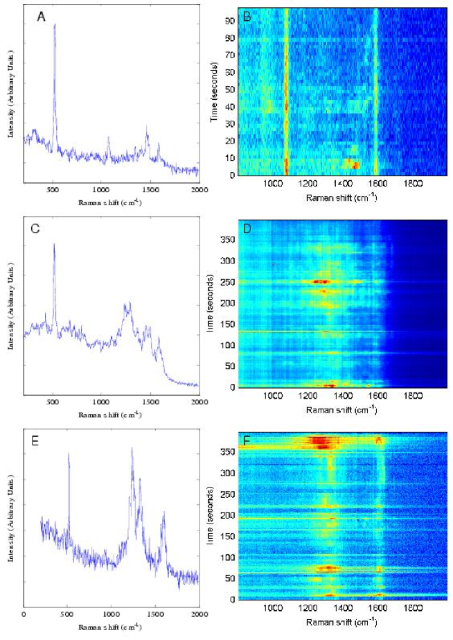
We have examined SERS spectra for varying supernatant solution concentration during the assembly procedure. Ideally, successive dilutions of the solution should vary surface coverage of the assembled molecules. While molecular coverage on the edges of polycrystalline Au films is not readily assessed, we observe reproducible qualitative trends as concentration is reduced. For MBA molecules assembled from solutions in nanopure water, we have varied concentrations from 1 mM down to 100 pM. The fraction of junctions showing SERS distinct from carbon contamination remains roughly constant down to concentrations as low as 1 M. For our volumes and electrode areas, this is still expected to correspond to a dense coverage of 1 molecule per 0.19 nm2. At concentrations below 1 M, SERS spectra change significantly, while remaining distinct from those of carbon contamination: blinking occurs more frequently; modes of b2 symmetry rather than a1 symmetry appear more frequently; and the molecular peaks can be more than 100 larger than the high coverage case for the same integration times. These observations are qualitatively consistent with the molecules exploring different surface orientations at low coverages, and charge transfer/chemical enhancement varying with orientation. However, the actual coverage at the edges remains unknown.
The concentration of the solution used for assembling molecules on the nanogap surface strongly influences the form of the observed Raman spectrum as well as the rate and intensity of the mode blinking. Raman spectra of MBA were taken by soaking samples in 2 mL of different concentrations of MBA. Although for all of these concentrations there are enough molecules in solution to form a monolayer over the bowtie surface, significant differences in the spectra were observed. Fig. S3A shows a representative Raman spectrum for MBA at the nanogap for 1mM concentrations. The two carbon ring modes at 1077 cm-1 and 1590 cm-1 are clearly present along with a third peak at 1463 cm-1. The time spectra for this nanogap in Fig S3B. The 1077 cm-1 and 1590 cm-1 peaks are relatively stable and always present while other modes, such as the 1463 cm-1 mode, blink on and off for a few seconds at a time. As the concentration is decreased to 1 M, the MBA signal tends to be stronger with more intense blinking. Additionally the 1077 cm-1 mode is observed to disappear while the 1590 cm-1 mode remains. Additional modes begin to become more visible such as the 1265 cm-1 and 1480 cm-1 modes seen in Fig S3C. At even lower concentrations such as 1 nM, the MBA signal is again more intense with even more blinking as seen in Fig. S3F (which has been plotted with intensity on a log scale). The 1077 cm-1 mode is again unseen while the 1590 cm-1 mode begins to fluctuate in intensity even more. The blinking becomes much more intense with the intensity of the signal periodically reaching close to ten times the maximum intensity observed for MBA at 1 M. We suggest that the increased blinking and larger amplitude signals are a result of the molecules not being as tightly packed on the surface in the 1 M and 1 nM cases as in the 1 mM case. As a result of looser packing, the molecules are free to explore more surface conformations, including those with more and different charge transfer with the Au surface.
We point out that these MBA spectra are distinct from those seen in physisorbed carbon contamination on initally clean junctions. These data persist at high incident powers and do not show “arrival” phenomena as described in the subsequent section. Furthermore, they are unlikely to originate from photodecomposition of MBA, since the illumination conditions are identical for all coverages.
IV Detection of adsorbed contaminants
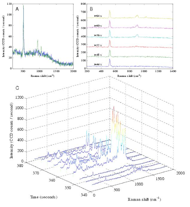
Due to the large enhancements possible with the nanogaps, contamination from airborne absorbates occurs readily in the absence of assembled molecules on the nanogap surface. We have observed the absorption of contaminants onto the surface of clean nanogaps in as little as 10 minutes. Collecting Raman spectra every 4 seconds, we can observe the appearance of contaminants on the surface as seen in Fig. S4A and S4B. It is difficult to identify the contaminants, as the spectra observed have large variations, although carbon ring modes are often observed in conjunction with other modes. Furthermore the Raman signal from contaminants often blinks very strongly, with periods of no or weak signal followed by several seconds of intense blinking, as seen in Fig S4C. The changes in intensity can be more than a factor of 100. Again we suggest that the strong blinking is a result of the weak attachment of the contaminants to the nanogap surface, allowing them to move considerably and explore many interactions with the Au surface. As previously mentioned, these contamination spectra are not observed when molecules of interest have been preassembled deliberately on the electrode surface. The likely explanation for this is that the self-assembled later sterically prevents contaminants from arriving at the nanogap region of maximum field enhancement.
V FDTD calculations
The optical properties of the bowtie structure were calculated using the Finite-Difference Time-Domain method (FDTD) using a Drude dielectric function with parameters fitted to the experimental data for gold. This fit provides an accurate description of the optical properties of gold for wavelengths larger than 500 nm [S1]. These calculations do not account for reduced carrier mean free path due to surface scattering in the metal film, nor do they include interelectrode tunneling. However, such effects are unlikely to change the results significantly.
The bowtie is modeled as a two finite triangular structures as illustrated in Fig. 4A of the manuscript. Our computational method requires the nanostructures to be modeled to be of finite extent. The plasmon modes of a finite system are standing modes with frequencies determined by the size of the sample and the number of nodes of the surface charge distribution associated with the plasmon. For an extended system such as the bowties manufactured in this study, the plasmon resonances can be characterized as traveling surface waves with a continuous distribution of wavevectors.
A series of calculations of bowties with increasing length reveals that the optical spectrum is characterized by increasingly densely spaced plasmon resonances in the wavelength regime 500-1000 nm and a low energy finite-size induced split-off state involving plasmons localized on the outer surfaces of the bowtie. For a large bowtie, we expect the plasmon resonances in the 500-1000 nm wavelength interval to form a continuous band [S2].
The electric field enhancements across the bowtie junction for the plasmon modes within this band are relatively similar with large and uniform enhancements in the range of 50-150. The magnitudes of the field enhancements were found to increase with increasing size of the bowtie structure. For instance, the maximum field enhancement factor was found to be 115 for a 200 nm bowtie (Each half of the bowtie is modeled as a truncated triangle 200 nm long.) and 175 for a 400 nm bowtie. Our use of a finite gridsize also underestimates the electric field enhancements[S3]. Thus our calculated electric field enhancements are likely to significantly underestimate the actual electric field enhancements in the experimentally manufactured bowties.
For a perfectly symmetric bowtie, significant field enhancements are only induced for incident light polarized across the junction. If the mirror symmetry is broken, for instance by making one of the structures thicker or triangular, large field enhancements are induced for all polarizations of incident light.
To investigate the effects of nanoasperities, FDTD calculations were performed for a bowtie with two semi-spherical protrusions in the junction as shown in Fig. 4 of the main text, and Figs. S5-S7 of the Supporting Online Material. As expected, the presence of these protrusions does not influence the optical spectrum. However, the local field enhancements around the protrusions become very large, typically three or four times higher than for the corresponding structure without the defect. The physical mechanism for this increase is an antenna effect caused by the coupling of plasmons localized on the protrusion with the extended plasmons on the remaining bowtie structure [S4].
VI Enhancement estimate
To estimate an enhancement based on the data of Fig. 3 in the main text, it was necessary to understand the effective count rate per molecule of Raman scattering from bulk MA in our measurement setup. This requires knowing the effective volume probed by the WITec system when the laser is focused on a bulk MA crystal.
The full-width-half-maximum (FWHM) of the laser spot size was found to be 575 nm. This was determined by measuring the count rate of the Rayleigh scattering peak (at zero wavenumbers) as a function of position as the beam was scanned over the edge of a Au film on a Si substrate. Averaging 16 such scans, the Rayleigh intensity was fit to the form of an integrated gaussian to determine the FWHM of the gaussian beam. The 575 nm figure is likely an overestimate due to systematic noise in the flat regions of the fit.
For a gaussian beam with intensity of the form , the FWHM . The effective radius of an equivalent cylindrical beam is , or 346 nm in this case. The effective confocal depth [S5] was determined by measuring the 520 cm-1 Si Raman peak as a function of vertical displacement of a blank substrate. The effective depth profile was determined by numerical integration of the Si data using matlab. The effective volume probed by the beam is cm3. From the bulk properties of MA, this corresponds to molecules.
The count rate for the bulk MA 1077 cm-1 line, corrected by the ratio of (Si SERS rate/Si bulk rate) to accomodate for the difference in laser powers, is 46 counts/s, compared with 203 counts/s for the SERS data of Fig. 3. This leads to the enhancement estimate quoted in the main text of .
[S1] Oubre, C.; Nordlander, P. J. Phys. Chem. B 108, 108, 17740-17747.
[S2] Nordlander, P.; Le, F. Appl. Phys. B 2006, 84, 35-41.
[S3] Oubre, C.; Nordlander, P. J. Phys. Chem. B 2005, 109, 10042-10051.
[S4] Hao, F.; Nehl, C. L.; Hafner, J. H.; Nordlander, P. Nano Lett. 2007, 7, 10.1021/nl062969c.
[S5] Cai, W.B.; Ren, B.; Li, X. Q.; Shi, C. X.; Liu, F. M.; Cai, X. W.; Tian, Z. Q. Surf. Sci. 1998, 406, 9-22.