Counterflow of electrons in two isolated quantum point contacts
Abstract
We study the interaction between two adjacent but electrically isolated quantum point contacts (QPCs). At high enough source-drain bias on one QPC, the drive-QPC, we detect a finite electric current in the second, unbiased, detector-QPC. The current generated at the detector-QPC always flows in the opposite direction than the current of the drive-QPC. The generated current is maximal, if the detector-QPC is tuned to a transition region between its quantized conductance plateaus and the drive-QPC is almost pinched-off. We interpret this counterflow phenomenon in terms of an asymmetric phonon-induced excitation of electrons in the leads of the detector-QPC.
pacs:
73.23.-b, 73.23.Ad, 73.50.LwThe state of a confined quantum system is modified by interactions with an external field (or with external sources of energy). In semiconductor nanostructures the energy and quasi-momentum of electrons acting as probe are strongly influenced by the environment, e. g. via electron-electron or electron-phonon interaction. If driven out of equilibrium, Coulomb forces establish the local equilibrium within the electron system whereas electron-phonon interactions dominate the energy exchange with the environment gantmakherlevinson . Drag experiments in semiconductor nanostructures provide a tool to study the effect of external electrons or phonons onto a probe electron system.
Current drag between parallel two-dimensional (2D) electron layers has been investigated in GaAs/AlGaAs bilayer systems. At small interlayer separations, observations are consistent with the Coulomb drag phenomenon gramila . At larger separations virtual-phonon exchange has been invoked to explain the data rubel95 . A negative sign of a current drag between 2D and 3D electron gases in GaAs was explained by the Peltier effect solomon . At high filling factors in a perpendicular magnetic field a sign change of the longitudinal drag between parallel 2D layers was found as a function of the imbalance of the electron density in the two layers feng ; lok .
Interactions between two lateral quantum wires in GaAs have been investigated in Ref. zverev . The observed frictional drag, strongly oscillating as a function of the one-dimensional (1D) subband occupation, was interpreted in terms of Coulomb interaction between two Luttinger liquids. Recently, the observation of negative Coulomb drag between two disordered lateral 1D wires in GaAs in perpendicular magnetic fields was reported tarucha .
Here we report on a novel interaction effect between two neighboring quantum point contacts (QPCs), embedded in mutually isolated electric circuits. When a strong current is flowing through the partially transmitting drive-QPC, we detect a small current in the second, unbiased, detector-QPC. The detector current flows in the opposite direction of the drive current and shows a nonlinear dependence on the source-drain bias of the drive-QPC. It oscillates as a function of the detector-QPC transmission. We suggest an explanation of this counterflow phenomenon in terms of asymmetric phonon-induced excitation of ballistic electrons in the leads of the detector-QPC.
Our samples are prepared on a GaAs/AlGaAs heterostructure containing a two-dimensional electron gas nm below the surface, with an electron density of cm-2 and a low-temperature mobility of cmVs. An AFM micrograph of the split-gate nanostructure, produced with e-beam lithography, is shown in the left inset of Fig. 1. The negatively biased central gate C divides the electron system into two separate circuits, and prevents leakage currents between them. Two QPCs are defined on the upper and lower side of the central gate, respectively, by biasing gates 8 and 3. Other gates are grounded if not stated otherwise.
The right inset of Fig. 1 shows a sketch of the counterflow experiment. We use separate electric circuits for the (upper) drive-QPC and (lower) detector-QPC. A dc bias voltage, , is applied to the left lead of the drive-QPC, while the right lead is grounded. A current-voltage amplifier with an input voltage-offset of about 10 V is connected to the right lead of the detector-QPC. Its left lead is always maintained at the same offset potential in order to assure zero voltage drop across the detector-QPC. In both circuits, a positive sign of the current corresponds to electrons flowing to the left. For differential counterflow conductance measurements, the drive bias is modulated at a frequency of 21 Hz and the resulting ac current component in the detector circuit is measured with lock-in detection in the linear response regime. All measurements are performed in a dilution refrigerator at an electron temperature below 150 mK. The experimental results are the same if detector and drive QPC are interchanged.
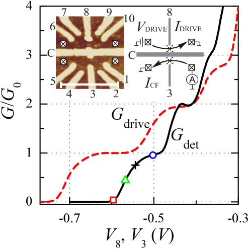
First, we characterize the QPCs using a standard differential conductance measurement. Figure 1 displays the differential conductances of both QPCs in linear response, measured as a function of the respective gate voltage , or . At low gate voltages, the QPCs are pinched-off and the conductance is close to zero. With increasing gate voltage, 1D channels successively open up vanwees_wharam . For both QPCs we observe three conductance plateaus approximately quantized in units of e2/h. With high bias spectroscopy kristensen we find the spacing between the two lowest subbands to be approximately 4 meV (3 meV) for the drive (detector) QPC. The half-width of the energy window for opening a 1D subband is meV in both QPCs.
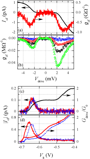
Having characterized the QPCs, we turn to counterflow measurements. Fig. 2a shows the dc counterflow current, , through the detector-QPC and the differential counterflow conductance, , as a function of the bias on the drive-QPC. Here, the drive-QPC is tuned to nearly half a conductance quantum , while the detector-QPC is in the pinch-off regime (i.e. the lowest 1D subband bottom is well above the Fermi level) with . Surprisingly, for mV, a finite current is observed in the unbiased detector circuit. The direction of is opposite to that of the drive-QPC current . The dc counterflow current is a threshold-like, nearly odd function of . Correspondingly, the differential counterflow conductance is negative and a nearly even function of . The sign of expresses a phase shift of between the applied ac modulation of and the detected ac component of the counterflow current.
Figures 2c and 2d show the absolute value of for the nearly pinched-off detector as a function of the voltage on gate 8, which tunes the drive-QPC transmission. The corresponding drive-QPC differential conductance curves are also shown. For not too high (Fig. 2c), a non-zero counterflow current is only detected in the region between pinch-off and the first conductance plateau of the drive-QPC. For higher (Fig. 2d) increases superlinearly with at its maximum and remains finite at higher gate voltages . Since the source bias effects the potential distribution near the constriction, the nonlinear conductance plateau of the drive-QPC shifts when changing glazmann . This causes the shift of the extrema on Fig. 2d as well as the asymmetry of in Fig. 2a when reversing the bias.
We proceed to study the counterflow effect in the regime of a more opened detector-QPC. Figure 2b plots remark1 as a function of for several values of between 0 and (marked with the same symbols in Fig. 1). The qualitative appearance of is independent of . However, the amplitude of is a strongly non-monotonic function of the detector transmission. The counterflow conductance reaches its maximum for and decreases rapidly with further increasing . Note that the absolute value of is small, corresponding to a maximal ratio of the counterflow and drive currents .
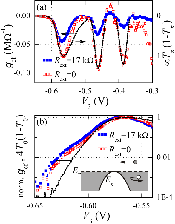
In Fig. 3a is plotted as a function of , controlling the detector transmission. and are adjusted for maximal and kept fixed. Confirming the trend seen in Fig. 2b, the measured (solid symbols) strongly oscillates with increasing and displays three pronounced maxima before the detector-QPC is fully opened. The position of the n-th maximum (n = 0,1,2) is close to the value of , where (Fig. 1). Here, the energy of the bottom of the n-th 1D subband of the detector-QPC aligns with the Fermi level of the leads . In contrast, is close to zero for fully transmitting 1D channels (). The overall magnitude of decreases with increasing , hence . This is caused by a finite series resistance of the external circuit, which results in a measured lower than the case for an ideal ammeter remark2 . The corrected counterflow conductance, , corresponding to , is shown in Fig. 3a with open symbols. The corrected maxima are roughly equal in size and symmetric. Moreover, the shape of the n-th maximum compares quite well with the corresponding function of the equilibrium transmission , extracted from the detector conductance data (dashed lines in Fig. 3a).
In Figure 3b we plot the normalized and the transmission function on a logarithmic scale near the detector pinch-off. In the pinch-off regime (i.e. for ) the transmission probability of a QPC is expressed as glazmann . Here is the kinetic energy of current carrying electrons and is the half-width of the energy window for opening a 1D-subband. The energy of the detector-QPC is controlled by gate 3 via . This explains a nearly exponential drop of the transmission function with decreasing (Fig. 3b). In contrast, the measured drops considerably slower and remains finite even where the detector-QPC is already pinched-off in equilibrium. This experimentally observed excess contribution of the normalized versus signals that the counterflow current carrying electrons are excited well above the Fermi level. Converting the shift in gate voltage (see the bar in Fig. 3b) to energy, we find a characteristic excitation energy of meV. This is consistent with a recently reported 1 meV bandwidth excitation provided by the drive-QPC for electrons in a nearby double-dot quantum ratchet DQDratchet .
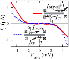
Next we study the counterflow effect between spatially shifted QPCs. Figure 4 shows through the nearly pinched-off detector-QPC as a function of the bias on the drive-QPC, which is formed either with gate 10 or gate 6, while gate 8 is now grounded (Fig. 1). Despite the shift of the drive-QPC position relative to the detector-QPC by about 300 nm, the odd drive bias dependence of the counterflow current found in Fig. 2 is practically preserved. This indicates that the excitation of electrons in one of the leads of the detector-QPC is not restricted to the close vicinity of the drive-QPC.
The oscillations of the counterflow conductance in Fig. 3 are reminiscent of thermopower oscillations that have been investigated on individual QPCs molenkamp ; dzurak . This suggests that is caused by an energetic imbalance across the detector-QPC. If the bottom of the -th 1D-subband of the detector-QPC is well separated from the Fermi-energy in comparison to the characteristic excitation energy, i. e. if , this subband is either fully transmitting () or closed (). In both cases electrons (holes) excited by above (below) are equally transmitted and . In contrast, if excited electrons are more likely transmitted than excited holes (see inset of Fig. 3b), resulting in .
The energetic imbalance across the detector-QPC we propose to be caused by phonon-based energy transfer from the drive-QPC. The excess energy of carriers injected across the drive-QPC is mainly relaxed by emission of acoustic phonons. We consider the drive-QPC in the non-linear regime near pinch-off where and the transmission probability is strongly energy-dependent (the source and drain leads are defined so that their chemical potentials satisfy ). In this case electrons injected into the drain lead have an excess energy of about whereas the source lead remains essentially in thermal equilibrium heiblum . Hence acoustic phonons are predominantly generated in the drain lead of the drive-QPC. Because of this asymmetry electron-hole pairs are excited preferentially in the adjacent lead of the detector-QPC remark3 . This gives rise to directed opposite to the current through the drive-QPC (and ). The data in Fig. 2 clearly show, that the counterflow effect is only observed in the non-linear regime of the drive-QPC.
For a rough estimate we consider injected electrons with a momentum relaxation time of 60 ps limited by elastic scattering and an energy relaxation time of 1 ns Ridley ; verevkin . Assuming isotropic phonon emission we estimate an energy transfer ratio which can account for the observed value of within one order of magnitude.
In summary, the current in a strongly biased drive-QPC generates a current flowing in the opposite direction through an adjacent unbiased detector-QPC. This counterflow current is maximal in between the conductance plateaus of the detector-QPC. The effect is most pronounced near pinch-off of the drive-QPC, where it behaves strongly non-linear. We interpret the results in terms of an asymmetric phonon-based energy transfer.
The authors are grateful to V.T. Dolgopolov, A.W. Holleitner, C. Strunk, F. Wilhelm, I. Favero, A.V. Khaetskii, N.M. Chtchelkatchev, A.A. Shashkin, D.V. Shovkun and P. Hänggi for valuable discussions and to D. Schrer and M. Kroner for technical help. We thank the DFG via SFB 631, the BMBF via DIP-H.2.1, the Nanosystems Initiative Munich (NIM) and VSK the A. von Humboldt foundation, RFBR, RAS, and the program ”The State Support of Leading Scientific Schools” for support.
References
- (1) V. F. Gantmakher and Y. B. Levinson, in Carrier Scattering in Metals and Semiconductors (North-Holland, Amsterdam, 1987)
- (2) T.J. Gramila et al., Phys. Rev. Lett. 66, 1216 (1991)
- (3) T.J. Gramila et al., Phys. Rev. B 47, 12957 (1993); H. Rubel et al., Semicond. Sci. Technol. 10, 1229 (1995)
- (4) B. Laikhtman et al., Phys. Rev. B. 41, 9921 (1990)
- (5) X.G. Feng et al., Phys. Rev. Lett. 81, 3219 (1998)
- (6) J.G.S. Lok et al., Phys. Rev. B 63, 041305 (2001)
- (7) P. Debray et al., J. Phys.: Condens. Matter 13, 3389, (2001); P. Debray et al., Semicond. Sci. Technol. 17, R21, (2002)
- (8) M. Yamamoto et al., Science 313, 204, (2006)
- (9) B.J. van Wees et al., Phys. Rev. Lett. 60, 848 (1988); D.A. Wharam et al., J. Phys. C 21, L209 (1988)
- (10) A. Kristensen et al., Phys. Rev. B 62, 10950 (2000)
- (11) L.I. Glazman, A.V. Khaetskii JETP Lett. 48 591 (1988)
- (12) For increasing the noises in the detector circuit increase, making the dc measurements very difficult.
- (13) The input resistance of the I-V amplifier, the ohmic contacts and wiring resistances result in k. The validity of the above formula has been checked by applying an additional 47 k resistor in series to .
- (14) V.S. Khrapai et al., Phys. Rev. Lett. 97, 176803 (2006)
- (15) L.W. Molenkamp et al., Phys. Rev. Lett. 68, 3765 (1992); H. van Houten et al., Semicond. Sci. Technol. 7, B215 (1992)
- (16) A.S. Dzurak et al., J. Phys.: Condens. Matter 5, 8055, (1993)
- (17) A. Palevski et al., Phys. Rev. Lett. 62, 1776 (1989); for asymmetric heat production in 3D point contacts see U. Gerlach-Meyer, H.J. Queisser Phys. Rev. Lett. 51, 1904 (1983)
- (18) is reduced for () and the drive-QPC shifted to the lh (rh) side of the detector-QPC (Fig. 4). This is understood in terms of absorption of phonons in both leads of the detector-QPC.
- (19) B.K. Ridley, Rep. Prog. Phys 54, 169 (1991)
- (20) A.A. Verevkin et al., Phys. Rev. B 53, R7592 (1996)